 Open Access Article
Influence of growth temperature on titanium sulphide nanostructures: from trisulphide nanosheets and nanoribbons to disulphide nanodiscs
Mohammad Talib,
Rana Tabassum,
S. S. Islam and
Prabhash Mishra *
*
Centre for Nanoscience and Nanotechnology, Jamia Millia Islamia (A Central University), New Delhi-110025, India. E-mail: pmishra@jmi.ac.in; Tel: +91-011-2698-1717, extn 3229
First published on 2nd January 2019
Abstract
We report the fabrication and characterization of titanium sulphide nanostructures using a chemical vapour transport (CVT) method. In CVT, reactions occur between titanium and sulphur powder in the vapor phase for TiSx nanostructure growth. Systematic studies on the effect of temperature, consequent structural evolution and optical properties were investigated by various characterization techniques. A series of experiments were performed by maintaining a fixed compositional ratio (1![[thin space (1/6-em)]](https://www.rsc.org/images/entities/char_2009.gif) :
:![[thin space (1/6-em)]](https://www.rsc.org/images/entities/char_2009.gif) 3) of Ti and S within a temperature range from 400 °C to 650 °C. On increasing the temperature from 400 °C to 650 °C; a gradual change in morphology was obtained from nanosheets (NS) to mixed phase nanoribbons and nanosheets (NS: NR), nanoribbons (NR), and nanodiscs (ND) of titanium sulphide, which was confirmed using SEM/TEM analysis. Then, the composition of titanium sulphides was studied using XRD, EDX and Raman spectroscopic techniques and it is observed that NS, NR and NS: NR have the composition ratio of TiS3 whereas ND has a ratio of TiS2. The phenomenon of decomposition of TiS3 into TiS2 at elevated temperatures was explained using thermogravimetric analysis (TGA) and differential thermal analysis (DTA) along with pictorial representations. The optical properties of the prepared TiS3/TiS2 nanostructures were studied using UV-vis and photoluminescence spectroscopy. It is concluded that composition ratio of Ti and S as well as the temperature variation plays a crucial role in the formation of different Ti–S nanostructures with unique optical, electronic and thermal properties.
3) of Ti and S within a temperature range from 400 °C to 650 °C. On increasing the temperature from 400 °C to 650 °C; a gradual change in morphology was obtained from nanosheets (NS) to mixed phase nanoribbons and nanosheets (NS: NR), nanoribbons (NR), and nanodiscs (ND) of titanium sulphide, which was confirmed using SEM/TEM analysis. Then, the composition of titanium sulphides was studied using XRD, EDX and Raman spectroscopic techniques and it is observed that NS, NR and NS: NR have the composition ratio of TiS3 whereas ND has a ratio of TiS2. The phenomenon of decomposition of TiS3 into TiS2 at elevated temperatures was explained using thermogravimetric analysis (TGA) and differential thermal analysis (DTA) along with pictorial representations. The optical properties of the prepared TiS3/TiS2 nanostructures were studied using UV-vis and photoluminescence spectroscopy. It is concluded that composition ratio of Ti and S as well as the temperature variation plays a crucial role in the formation of different Ti–S nanostructures with unique optical, electronic and thermal properties.
1. Introduction
Chalcogenides (chemical compounds) are defined in such a way that they partially possesses one chalcogen anion and one electropositive element in their chemical formula [(MCx), M stands for metal, C is chalcogen and x is a number]. In the periodic table, group 16 elements are considered as chalcogens. Generally, the term chalcogenide is reserved for sulphides, selenides, tellurides, and polonides but at the same time many metal ores also exists as chalcogenides. Nowadays, the most commonly used chalcogenides in research are MOS2, WS2, TiS3, TiS2 etc. The redox chemistry of titanium sulphide (Ti–S) has attracted renewed interest in the fabrication of various types of nanostructures ranging from 3D to 1D. This is due to the fact that Ti–S acts as a host matrix for intercalation.1–8 Ti–S nanostructures are used in several applications such as hydrogen storage, lithium intercalation, synthesis of lubricants, glassware, chemical and bio-sensing, etc.9,10 The 2D nanostructures of TiS3 can be a suitable replacement for silicon based devices for applications where high optical gain is required.11–19 It has been reported that the fabricated Ti–S nanostructures may have the composition as titanium trisulphide (TiS3) and titanium disulphide (TiS2). Although, the nanotechnology enabled properties of both titanium trisulphide (TiS3) and titanium disulphide (TiS2) are found to be relatively unexplored.20,21 TiS3 contains infinite distorted trigonal prism chains which are aligned parallel to its monoclinic b axis and it is semiconducting in nature with a band gap of ≈1.1 eV. In addition to several 2D materials, graphene and chalcogenides such as MoS2, WS2, TiS3, TaS3, NbS3, NbSe3 etc. possesses unusual electrical, thermal, optical, and mechanical properties etc.,22 one of the properties that they exhibit is weak out-of-plane bonding between layers by which they can be exfoliated using simple exfoliation techniques such as mechanical or liquid exfoliation. Specifically, TiS3 has a modest band gap, higher carrier mobility, and better anisotropic, electronic and optical properties.23–25Recently, many reports have been found on the fabrication and characterization of TiS3 nanobelts with its several exciting properties such as high tensile strength, good optical properties, better field emission properties etc.26,27 Till date, various growth studies have been found on the titanium sulphides production in a highly controllable and reproducible way. These methodologies can also be used in batch production of Ti–S nanostructures. One such method to fabricate Ti–S nanomaterials is using precursor reduction–sulfurization reactions resulting in well-defined synthesis of TiS2 nanotubes with diameters of about 10 nm and lengths upto 5 μm. This method includes the reaction of a precursor [titanium tetrachloride (TiCl4)] in presence of H2S and H2 gas.28 However, chemical vapour deposition (CVD) is another technique to synthesise TiS3 and TiS2 nanostructures, but only few reports are available till now. The limitation of this method is that it produces some unusual by-products such as complex secondary structures in addition to desired primary structures (Ti–S nanostructures). Wet chemical method is yet another method to fabricate Ti–S nanostructures resulting in synthesis of flower-like structure.29,30 These dendrimers (flowers) like nanostructures are found to originate from stoichiometric quantities of the powdered Ti and S. In the fabrication of nanoflower array structures, titanium foil substrate is needed. The obtained results have been optimised in terms of growth temperatures and reaction times in order to achieve the consistent morphology, crystallographic structure and purity. Recent study suggests that by utilising a Ni-coated Si wafer as a growth substrate whiskers of TiS2 can be fabricated.31 Here, the substrate was placed in between sulphur and titanium sources and the synthesis was carried out under a stream of argon gas. In another recent method, nickel was used as a catalyst in a vapour-liquid-solid (VLS) mechanism leading to the fabrication of stoichiometric TiS2 whiskers with inner diameters ranging from 100–200 nm. These fabrication methods possess their own advantages and disadvantages such as some releases by-products in addition to desired nanostructures; some do not produce desired size and properties. Thus, a new approach has been developed for the fabrication of Ti![[thin space (1/6-em)]](https://www.rsc.org/images/entities/char_2009.gif) :
:![[thin space (1/6-em)]](https://www.rsc.org/images/entities/char_2009.gif) S nanostructure known as chemical vapour transport (CVT).26,27 The advantages of CVT method includes ease of fabrication, controlled morphology and batch production. Using CVT method, TiS3 and TiS2 nanostructures can be fabricated because both Ti and S have relatively lower melting point which allows easy reaction and transportation of their vapours in the form of nanostructures. Although it has been reported that thin films of TiS3 can be formed under low temperature conditions by CVT method by utilizing TiCl4 as a precursor but detailed fabrication of titanium trisulphide nanostructures is not investigated.31
S nanostructure known as chemical vapour transport (CVT).26,27 The advantages of CVT method includes ease of fabrication, controlled morphology and batch production. Using CVT method, TiS3 and TiS2 nanostructures can be fabricated because both Ti and S have relatively lower melting point which allows easy reaction and transportation of their vapours in the form of nanostructures. Although it has been reported that thin films of TiS3 can be formed under low temperature conditions by CVT method by utilizing TiCl4 as a precursor but detailed fabrication of titanium trisulphide nanostructures is not investigated.31
It is a focus of our research work to report chemical vapour transport (CVT) method to fabricate the nanostructures of TiS3 as well as TiS2 using Ti and S powder. The temperature plays a crucial role in the fabrication of different 2D nanostructures in a controlled way. In CVT method, metal surfaces or metal powders are used as a growth medium and hence researchers have explored CVT method for the fabrication of nanostructures. In general, CVT method is used to grow chalcogens based nanostructures the materials have been used in the vapour phase over a suitable metal substrate32–34 but if we use the powder form of chalcogens in place of their substrate then it would provide the ease of fabrication and it would reduce the cost of fabrication.
In this paper, we describe CVT method to fabricate titanium sulphide nanostructures with different morphologies and properties. In this method, titanium and sulphur powder in a specified ratio were allowed to react with each other in a vacuum sealed ampoule. The product in ampoule was then heated at different temperatures ranging from 400 °C to 650 °C. Due to heating, reactions occurs between titanium and sulphur powder to form TiSx, the specimen is thus transported in the vapour phase to grow its nanostructures. The beauty of this method is to fabricate various Ti–S nanostructures such as from nanoribbons to nanodiscs. The techniques permit fabrication of Ti–S nanostructures with control phase, defined crystal structure as well as morphology. Systematic studies on effects of growth temperatures, consequent structural/morphological evolution as well as optical properties were examined by various characterization techniques. The experiments were performed for different composition ratio of Ti and S at different temperatures. The structural and morphological properties were investigated using SEM and TEM. The optical properties of the prepared Ti–S nanostructures were investigated using UV-vis and photoluminescence spectroscopy. The composition of Ti–S has been determined using XRD, EDX and Raman spectroscopic techniques. Finally, the phenomenon of decomposition of Ti–S at elevated temperature has been explained in detail using TGA/DTA analysis.
2. Experimental
2.1 Chemicals and reagents
Titanium powder (purity 99.95% of 100 mesh was purchased from Good fellow) and sulphur powder (purity 99.99% of −100 mesh was purchased from Fisher scientific). Both the chemicals were used as received without any further modification or purification. Glass ampoule of 12 mm diameter was purchased from local vendor whereas deionizing water procured from Millipore® and acetone was used for cleaning purpose during experimentation.2.2 Fabrication of Ti–S nanostructures
Chemical vapour transport (CVT) method was adopted for the fabrication of titanium sulphide (Ti–S) nanostructures. The detail description of the fabrication process of Ti–S nanostructures using CVT is shown in Fig. 1. In this process, firstly titanium (Ti) powder and sulphur (S) powder was mixed in a specified ratio typically 1![[thin space (1/6-em)]](https://www.rsc.org/images/entities/char_2009.gif) :
:![[thin space (1/6-em)]](https://www.rsc.org/images/entities/char_2009.gif) 3 by mass percent in pestle and mortar. After uniformly mixing the two components (Ti and S), mixture powder was transferred at one end of 12 mm diameter silica ampoule for reaction process as shown in step-1 of Fig. 1. Then the ampoule was vacuum sealed to a pressure of approximately 2 × 10⁻⁵ mbar using a vacuum sealing unit having a diffusion pump backed with a rotary pump which can give vacuum of the order of 10−5 mbar as shown in step-2 of Fig. 1. The vacuum sealing of ampoule was required to prevent the mixture inside it from moisture and oxidation during heating. Finally, sealed ampoule having the mixture of Ti and S was placed in a furnace at different temperatures from 400 °C to 650 °C for about 24 hours. In this way, 6 samples were prepared in the ratio of Ti
3 by mass percent in pestle and mortar. After uniformly mixing the two components (Ti and S), mixture powder was transferred at one end of 12 mm diameter silica ampoule for reaction process as shown in step-1 of Fig. 1. Then the ampoule was vacuum sealed to a pressure of approximately 2 × 10⁻⁵ mbar using a vacuum sealing unit having a diffusion pump backed with a rotary pump which can give vacuum of the order of 10−5 mbar as shown in step-2 of Fig. 1. The vacuum sealing of ampoule was required to prevent the mixture inside it from moisture and oxidation during heating. Finally, sealed ampoule having the mixture of Ti and S was placed in a furnace at different temperatures from 400 °C to 650 °C for about 24 hours. In this way, 6 samples were prepared in the ratio of Ti![[thin space (1/6-em)]](https://www.rsc.org/images/entities/char_2009.gif) :
:![[thin space (1/6-em)]](https://www.rsc.org/images/entities/char_2009.gif) S as 1
S as 1![[thin space (1/6-em)]](https://www.rsc.org/images/entities/char_2009.gif) :
:![[thin space (1/6-em)]](https://www.rsc.org/images/entities/char_2009.gif) 3 which were placed in furnace and heated one by one at temperature 400 °C, 450 °C, 500 °C, 550 °C, 600 °C and 650 °C respectively. For removing the products after reaction, the neck of the ampoule was cut with sharp quartz cutter which releases its pressure then the desired product was collected. In this procedure, certain post reaction precautions must be taken; firstly we must properly cover our eyes and hands to cut the ampoule. Secondly, the ampoule should not be hit by any object because it acts as a mini bomb due to high pressure of sulphur inside. After the reaction, different types of TiSx nanostructures have been obtained which has been depicted in Fig. 1.
3 which were placed in furnace and heated one by one at temperature 400 °C, 450 °C, 500 °C, 550 °C, 600 °C and 650 °C respectively. For removing the products after reaction, the neck of the ampoule was cut with sharp quartz cutter which releases its pressure then the desired product was collected. In this procedure, certain post reaction precautions must be taken; firstly we must properly cover our eyes and hands to cut the ampoule. Secondly, the ampoule should not be hit by any object because it acts as a mini bomb due to high pressure of sulphur inside. After the reaction, different types of TiSx nanostructures have been obtained which has been depicted in Fig. 1.
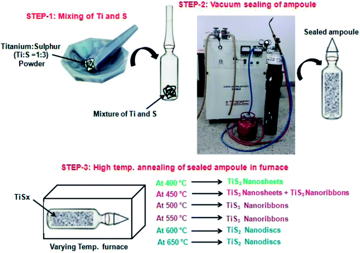 | ||
| Fig. 1 Schematic of the chemical vapour transport (CVT) method for the fabrication of titanium sulphide (Ti–S) nanostructures. | ||
2.3 Characterization of Ti–S nanostructures
Systematic characterizations of all the prepared samples of Ti![[thin space (1/6-em)]](https://www.rsc.org/images/entities/char_2009.gif) :
:![[thin space (1/6-em)]](https://www.rsc.org/images/entities/char_2009.gif) S were carried out. The investigations were carried out so as to get the growth effects, consequent structural/morphological evolution as well as the optical properties of Ti–S nanostructures. The complete investigation of structure/morphology of Ti–S nanostructures was carried out using scanning electron microscopy (SEM) and transmission electron microscopy (TEM). The optical properties were evaluated using UV-vis and photoluminescence spectroscopy. The composition of Ti and S was confirmed using X-ray diffraction, Raman and Energy dispersive X-ray spectroscopy. Finally, the effect of growth temperature on the morphology of the Ti–S nanostructures was investigated using thermogravimetric analysis (TGA) and differential thermal analysis (DTA).
S were carried out. The investigations were carried out so as to get the growth effects, consequent structural/morphological evolution as well as the optical properties of Ti–S nanostructures. The complete investigation of structure/morphology of Ti–S nanostructures was carried out using scanning electron microscopy (SEM) and transmission electron microscopy (TEM). The optical properties were evaluated using UV-vis and photoluminescence spectroscopy. The composition of Ti and S was confirmed using X-ray diffraction, Raman and Energy dispersive X-ray spectroscopy. Finally, the effect of growth temperature on the morphology of the Ti–S nanostructures was investigated using thermogravimetric analysis (TGA) and differential thermal analysis (DTA).
In order to perform SEM, we used Zeiss-SEM model Σigma version 5.05 system. Typical 6 samples were scanned which were loaded onto aluminium stubs using adhesive carbon tabs and performed in high vacuum mode. To further analyse the detailed morphology of all the samples, TEM was performed using a FEI Tecnai T20 (FEI, Eindhoven, Netherlands). For all the 6 samples TEM was operated at 300 kV acceleration voltage using a LaB6 filament with images recorded using a Megaview III CCD camera. In a typical operation of TEM, conventional bright field and dark field diffraction contrast imaging was used with selected area electron diffraction (SAED) to characterize the samples so as to relate it with the crystallography of the sample. To perform TEM, all the 6 samples were prepared in ethanol and then pipetting drops of the dispersion onto holey copper grids.
Energy dispersive X-ray (EDX) was performed using Bruker instrument of model Quantax. Using EDX, we can determine the elemental compositions with high accuracy. The beauty of the EDX analysis is that it can determine the presence of elements in the sample which are of atomic number from carbon upwards.
Again, to get the crystallographic information of the prepared samples, Powder X-ray diffraction (PXD) analysis was performed using a smart lab Rikagu with Cu Kα radiation (λ = 1.5418 Å) in flat plate geometry. To perform PXD, samples were loaded onto stub after subsequent cleaning of the stub with acetone so as to remove any impurities. Then the diffraction data were collected typically for 5° ≤ 2θ ≤ 80° with a 0.017° step size with scan times of about 2 h with a sample stage rotation of 15 rpm so as to get the best possible results.
In order to cross verify the composition of the prepared sample, we have performed Raman spectroscopy at room temperature using a Horiba Lab RAM HR 800, JY confocal microscope system with a 532 nm green laser. In typical Raman operation, hole aperture was kept typically 50 μm, 600 g mm−1 grating and a Synapse CCD detector were used.
To get the optical properties, UV-vis and photoluminescence spectra was obtained. UV-vis was obtained using Specord 210 Plus (Analytic Zena) which is a high-performance real double beam instruments with cooled double detection (CDD) system. In the measurements of UV-vis, the sample was used in the form of sonicated dispersion solution. All the samples were sonicated in ethanol individually and were placed in glass cuvette and the measurements were carried out in the visible region of electromagnetic spectrum. Similarly, the photoluminescence spectrum was obtained using Horiba Jobin Yvon instruments.
Again, the temperature dependent studies of all the samples were carried out using TGA 4000 Perkin Elmer. In this measurement, the temperature range was selected from 0° to 1000 °C which includes the temperature used in the fabrication process.
3. Results and discussion
In order to get the clear image and better understanding of the fabricated Ti–S nanostructures, we performed the scanning electron microscopy of all the prepared samples which has been discussed in Section 2.2. The SEM images shown in Fig. 2(a–d) shows the temperature dependent effects on the Ti–S nanostructures. These SEM images of Fig. 2(a) reveal that at growth temperature 400 °C, distinct nanosheets of Ti–S were observed. With the increase in growth temperature to 450 °C, nanosheets started to grow into the mixed phase of nanosheets and nanoribbons of Ti–S which is clearly shown in Fig. 2(b). From the growth temperature 500 °C, formation of individual nanoribbons started which continues until the temperature reaches to 550 °C which can be clearly noticed in Fig. 2(c and d). On further increasing the temperature as the temperature reaches to 600 °C, well-defined hexagonal nanodiscs formed which continues to form at temperature 650 °C also as shown in Fig. 2(e and f). By increasing the temperature more than 650 °C, Ti–S hexagonal nanostructures continues to observe which signs towards the over-growth due to the decomposition of Ti–S at higher temperature. From the SEM images given in Fig. 2, it is also evident that the growth of nanosheets, nanoribbons and nanodiscs are not continuous in nature. The reason for non-uniform surface coverage of hexagonal nanosheets over large area can be understood with the fact that TiS3 possess certain defects levels. The presence of defects levels will be discussed in further studies of this article. Therefore, by the studies of growth temperature, it can be concluded that on employing CVT method on the mixture of Ti and S, nanosheets, mixed phase nanosheets/nanoribbons as well as distinct nanoribbons and nanodiscs of titanium sulphide can be fabricated where the key point is the precise growth temperature which ranges from 400 °C to 650 °C.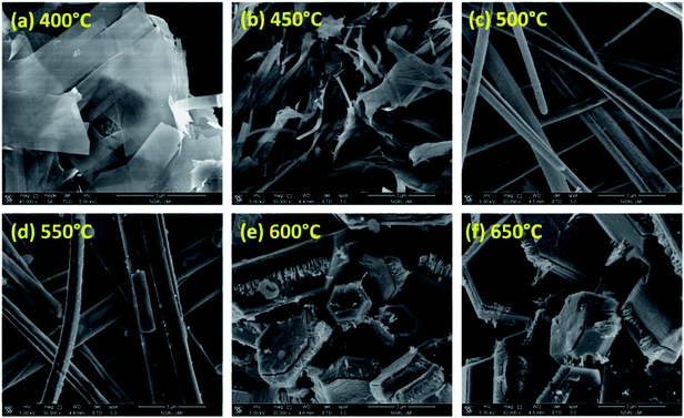 | ||
| Fig. 2 SEM image of the titanium sulphide (Ti–S) nanostructures grown at different temperature for 24 h at magnification of 3 μm (a) 400 °C (b) 450 °C (c) 500 °C (d) 550 °C (e) 600 °C (f) 650 °C. | ||
Further, to get the insight of morphology and the crystal structure of the fabricated Ti![[thin space (1/6-em)]](https://www.rsc.org/images/entities/char_2009.gif) :
:![[thin space (1/6-em)]](https://www.rsc.org/images/entities/char_2009.gif) S nanosheets, mixed phase nanosheets/nanoribbons, nanoribbons and nanodiscs, transmission electron microscopy (TEM) and selected area electron diffraction (SAED) was performed. In Fig. 3(a–r), TEM images of Ti–S nanostructures grown at temperature from 400 °C to 650 °C has been displayed. On close inspection of the micrograph of Fig. 3(a and b), nanosheets can be clearly observed which were fabricated at growth temperature 400 °C and from Fig. 3(c), SAED pattern displayed the planes of the Ti
S nanosheets, mixed phase nanosheets/nanoribbons, nanoribbons and nanodiscs, transmission electron microscopy (TEM) and selected area electron diffraction (SAED) was performed. In Fig. 3(a–r), TEM images of Ti–S nanostructures grown at temperature from 400 °C to 650 °C has been displayed. On close inspection of the micrograph of Fig. 3(a and b), nanosheets can be clearly observed which were fabricated at growth temperature 400 °C and from Fig. 3(c), SAED pattern displayed the planes of the Ti![[thin space (1/6-em)]](https://www.rsc.org/images/entities/char_2009.gif) :
:![[thin space (1/6-em)]](https://www.rsc.org/images/entities/char_2009.gif) S nanosheets grown at 400 °C. Similarly, when the growth temperature was kept 450 °C, mixed phase nanosheets/nanoribbons was formed which is shown in Fig. 3(d and e). The obtained planes of the mixed phase nanosheets/nanoribbons can be clearly visible in Fig. 3(f). Again, on further increasing the growth temperature in the range 500 °C to 550 °C, mixed phase nanosheets/nanoribbons turns into single phase nanoribbons and can be clearly noticeable in Fig. 3(g and h). The planes in the fabricated Ti
S nanosheets grown at 400 °C. Similarly, when the growth temperature was kept 450 °C, mixed phase nanosheets/nanoribbons was formed which is shown in Fig. 3(d and e). The obtained planes of the mixed phase nanosheets/nanoribbons can be clearly visible in Fig. 3(f). Again, on further increasing the growth temperature in the range 500 °C to 550 °C, mixed phase nanosheets/nanoribbons turns into single phase nanoribbons and can be clearly noticeable in Fig. 3(g and h). The planes in the fabricated Ti![[thin space (1/6-em)]](https://www.rsc.org/images/entities/char_2009.gif) :
:![[thin space (1/6-em)]](https://www.rsc.org/images/entities/char_2009.gif) S nanoribbons has been clearly shown in Fig. 3(i). The formation of Ti–S nanoribbons continues till the growth temperature reaches to 550 °C which is shown in Fig. 3(j and k) and its planer structure has been depicted in Fig. 3(l). On increasing the growth temperature to 600 °C, formation of nanoribbons will no longer persists but nanodiscs starts forming. The TEM images of the Ti
S nanoribbons has been clearly shown in Fig. 3(i). The formation of Ti–S nanoribbons continues till the growth temperature reaches to 550 °C which is shown in Fig. 3(j and k) and its planer structure has been depicted in Fig. 3(l). On increasing the growth temperature to 600 °C, formation of nanoribbons will no longer persists but nanodiscs starts forming. The TEM images of the Ti![[thin space (1/6-em)]](https://www.rsc.org/images/entities/char_2009.gif) :
:![[thin space (1/6-em)]](https://www.rsc.org/images/entities/char_2009.gif) S nanodiscs has been shown in Fig. 3(m and n) and the corresponding SAED patterns has been depicted in Fig. 3(o). On further increasing the growth temperature to 650 °C, the formation of nanodiscs will continue to form. The TEM images of the Ti
S nanodiscs has been shown in Fig. 3(m and n) and the corresponding SAED patterns has been depicted in Fig. 3(o). On further increasing the growth temperature to 650 °C, the formation of nanodiscs will continue to form. The TEM images of the Ti![[thin space (1/6-em)]](https://www.rsc.org/images/entities/char_2009.gif) :
:![[thin space (1/6-em)]](https://www.rsc.org/images/entities/char_2009.gif) S nanodiscs has been shown in Fig. 3(p and q) and the corresponding SAED pattern shown in Fig. 3(r) displays its planer structure.
S nanodiscs has been shown in Fig. 3(p and q) and the corresponding SAED pattern shown in Fig. 3(r) displays its planer structure.
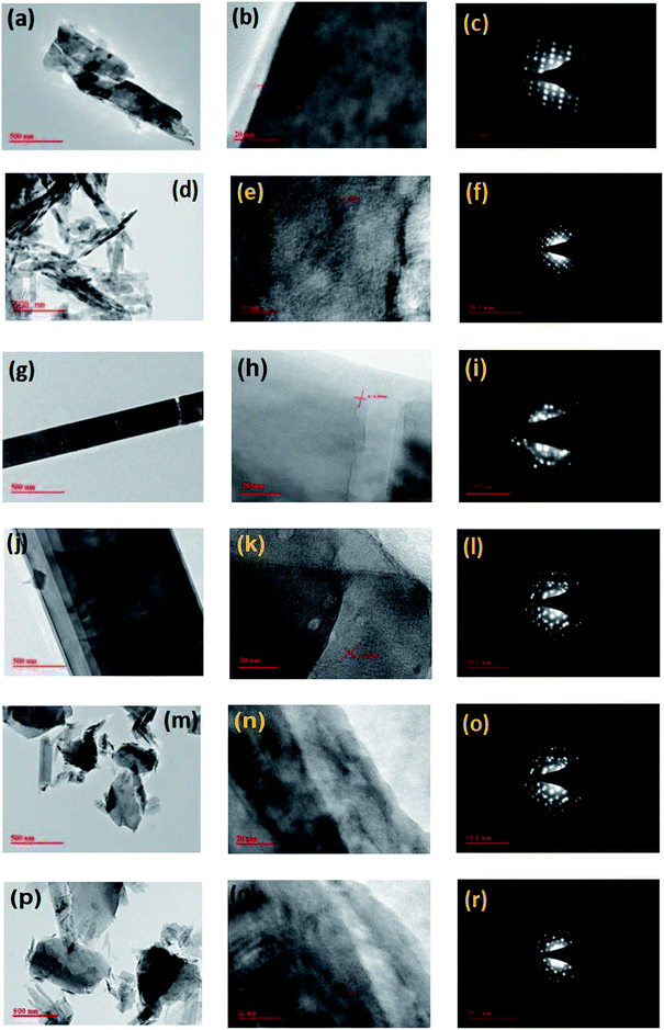 | ||
| Fig. 3 TEM/SAED image of the titanium sulphide nanostructures grown at different temperature for 24 h (a–c) 400 °C (d–f) 450 °C (g–i) 500 °C (j–l) 550 °C (m–o) 600 °C (p–r) 650 °C. | ||
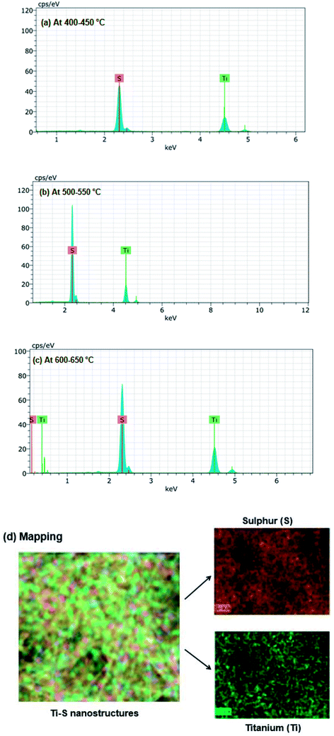
Once the formation of different types of Ti–S nanostructures at growth temperatures ranges from 400 °C to 650 °C has been confirmed, the investigation of elemental quantification of these Ti–S nanostructures was performed using energy dispersive X-ray (EDX). EDX is an efficient method for elemental analysis of the sample because EDX technique is non-destructive and specimens of interest can be examined in situ with little or no sample preparation. The data generated by EDX consists of spectra showing peaks corresponding to the elements making up the true composition of the sample being analyzed.35 EDX provides precise information of the weight percentage of the individual components in the Ti–S nanostructures. EDX was used to record the spectrum on a selected area covered by Ti–S nanostructures. EDX spectrum of the fabricated Ti–S nanostructures grown at temperature ranges from 400 °C to 650 °C is shown in Fig. 4(a–c). Fig. 4(a) shows the EDX spectrum for nanosheets and mixed phase nanosheets/nanoribbons fabricated at growth temperature 400 °C to 450 °C where the characteristic peaks of titanium (Ti) and sulphur (S) are clearly visible. Similarly, EDX spectrum of the nanoribbons and nanodiscs fabricated from 500 °C to 650 °C are shown in Fig. 4(b and c) where the characteristics peaks of Ti and S are also noticeable. The EDX data of all the Ti–S nanostructures is listed in Table 1. In the table, according to the weight percentage of Ti and S found in the nanosheets and mixed phase nanosheets/nanoribbons, the formation of TiS3 compound can be substantiated. In the mixed nanoribbons fabricated after growth at 500 °C and 550 °C, the percentage of Ti and S are found to be such that the formation of TiS3 has been confirmed. Further, if we notice the elemental percentage of Ti and S in the nanodiscs formed on growth at 600 °C and 650 °C, the formation of TiS2 has been confirmed. The noticeable point here is that the disc like nanostructure possesses the elemental composition of individual Ti and S in such a way that TiS2 get formed and all the other nanostructures i.e. nanoribbons and mixed phase nanoribbons and nanosheets possess the elemental composition of individual Ti and S in such a way that TiS3 get formed. On further increasing the growth temperature to 650 °C, the formation of TiS2 continues to occur. As the fabricated Ti–S nanostructures were deposited over the suitable substrate, EDX mapping was carried out over the dispersed area so as to quantify the element over the whole dispersed region. In Fig. 4(d) the EDX mapping indicated the spatial distribution of titanium and sulphur in particular area i.e. brown and green color shows distribution of titanium and sulphur respectively. From the mapping it may be noticeable that the color contrast between Ti and S is found to be in agreement with the atomic/weight percentage which is given in Table 1 for all the Ti–S nanostructures. This EDX studies also evident the formation of desired nanosheets, mixed phase nanosheets and nanoribbons, nanoribbons and nanodiscs requires precise optimization of growth temperature and analysis of growth mechanism.
| Temp. (°C) | Element | Series | Normalized (wt%) | Atomic (at%) | Chemical Formula |
|---|---|---|---|---|---|
| 400 | S | K | 66.60 | 75.17 | TiS3 |
| Ti | K | 33.40 | 24.83 | ||
| 450 | S | K | 66.46 | 77.43 | TiS3 |
| Ti | K | 33.54 | 22.43 | ||
| 500 | S | K | 67 | 75.23 | TiS3 |
| Ti | K | 33 | 24.77 | ||
| 550 | S | K | 66.71 | 76.33 | TiS3 |
| Ti | K | 33.29 | 23.67 | ||
| 600 | S | K | 58 | 65.64 | TiS2 |
| Ti | K | 42 | 34.36 | ||
| 650 | S | K | 57.35 | 66.30 | TiS2 |
| Ti | K | 42.65 | 33.70 |
In EDX, the formation of TiS3 and TiS2 has been explained which can further be validated using a well known empirical relationship. The relation shows the formation and stability of TiS3 by linking the partial pressure of sulphur with growth temperature given by eqn (1).36
log![[thin space (1/6-em)]](https://www.rsc.org/images/entities/char_2009.gif) P (mm Hg) = 10.42(±0.42) − 6850/T(±340) P (mm Hg) = 10.42(±0.42) − 6850/T(±340)
| (1) |
Under the above mentioned experimental condition in terms of temperature and composition, assuming Ti![[thin space (1/6-em)]](https://www.rsc.org/images/entities/char_2009.gif) :
:![[thin space (1/6-em)]](https://www.rsc.org/images/entities/char_2009.gif) S as 1
S as 1![[thin space (1/6-em)]](https://www.rsc.org/images/entities/char_2009.gif) :
:![[thin space (1/6-em)]](https://www.rsc.org/images/entities/char_2009.gif) 3, it was found that this composition was sufficient to prevent decomposition of TiS3 to TiS2 from temperature range 400 °C to 550 °C. These observations would agree with our elemental analysis (EDX) of the nanostructures grown at temperature from 400 °C to 550 °C. Keeping the Ti
3, it was found that this composition was sufficient to prevent decomposition of TiS3 to TiS2 from temperature range 400 °C to 550 °C. These observations would agree with our elemental analysis (EDX) of the nanostructures grown at temperature from 400 °C to 550 °C. Keeping the Ti![[thin space (1/6-em)]](https://www.rsc.org/images/entities/char_2009.gif) :
:![[thin space (1/6-em)]](https://www.rsc.org/images/entities/char_2009.gif) S ratio same as 1
S ratio same as 1![[thin space (1/6-em)]](https://www.rsc.org/images/entities/char_2009.gif) :
:![[thin space (1/6-em)]](https://www.rsc.org/images/entities/char_2009.gif) 3 and on increasing the growth temperature to 600 °C and 650 °C, the configuration (temperature and composition) would appear to be sufficient to decompose TiS3 to TiS2. Here it is noticeable that from successful PVT reactions given by eqn (1), it is observed that at elevated temperatures (650 °C) even at higher ratios of S to Ti such as 50
3 and on increasing the growth temperature to 600 °C and 650 °C, the configuration (temperature and composition) would appear to be sufficient to decompose TiS3 to TiS2. Here it is noticeable that from successful PVT reactions given by eqn (1), it is observed that at elevated temperatures (650 °C) even at higher ratios of S to Ti such as 50![[thin space (1/6-em)]](https://www.rsc.org/images/entities/char_2009.gif) :
:![[thin space (1/6-em)]](https://www.rsc.org/images/entities/char_2009.gif) 1 lead to decomposition of TiS3 resulting the formation of TiS2.
1 lead to decomposition of TiS3 resulting the formation of TiS2.
For the confirmation of crystallographic information of Ti–S nanostructures fabricated on growth temperatures ranges from 400 °C to 650 °C, Powder X-ray diffraction (PXRD) has been performed. The XRD pattern of the Ti–S nanostructures is shown in Fig. 5. The diffraction pattern of Ti–S nanostructure prepared on growth temperature from 400 °C to 550 °C shows mixed phase crystallinity with a prominent phase of monoclinic TiS3(analogous to JCPDS-ICDD 15–0783).18 However, at such a temperature an incomplete reaction may be possible and other diffraction peaks related to TiS3 may also visible. For growth temperatures from 600 °C to 650 °C, XRD pattern has been found to be consistent with TiS2 (ICDD no. 01-088-2479), with hexagonal unit cell parameters listed in Table 2. The diffraction peaks are found to be sharp and strong enough which confirms that the products obtained would be of pure phases and well crystallized. From the XRD pattern, it is also indicated that [001] direction should be the preferred direction for the growth of TiS2. The powder X-ray diffraction crystallographic data obtained for both TiS3 and TiS2 nanostructures has been detailed in Table 2 whereas the list of dominant peak corresponding to JCPDS data of TiS3 and ICDD data of TiS2 is given Table 3. The corresponding crystallographic information (listed in Table 2) confirms the monoclinic structure of the TiS3 and hexagonal structure of TiS2. From the crystallographic information, it may be noticeable that the products synthesized at 400 °C to 450 °C were confirmed to contain TiS3 nanosheets as well as TiS3 nanoribbons while those prepared at 500 °C to 550 °C were confirmed to contain pure TiS3 nanoribbons. The growth temperature 600 °C and 650 °C tended to produce TiS2 hexagonal discs of superior crystal quality. Further, in order to investigate the purity and perfect crystallization of the nanostructures obtained at different growth temperatures using the same CVT reactions, the XRD peaks for both TiS3 and TiS2 has been given in Table 3. Therefore, it may be concluded that the optimum growth temperature for pure TiS3 nanosheets appears to be 400 °C, pure TiS3 nanoribbons appears to be 500 °C to 550 °C whereas pure TiS2 hexagonal discs appears to be about 600 °C to 650 °C.
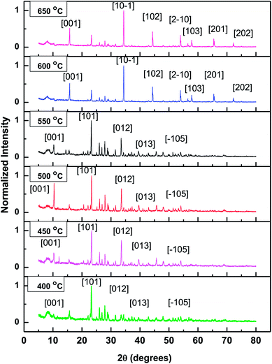 | ||
| Fig. 5 X-ray diffraction pattern of the fabricated titanium sulphide nanostructures grown at different growth temperature for 24 h. | ||
| Chemical formula | TiS3 | TiS2 |
|---|---|---|
| Annealed temperature | 400 °C to 550 °C | 600 °C to 650 °C |
| Crystal system | Monoclinic | Hexagonal |
| a (Å) | 5.02 | 3.39 |
| b (Å) | 3.46 | 3.39 |
| c (Å) | 8.79 | 5.66 |
| α (degree) | 90 | 90 |
| β (degree) | 97.73 | 90 |
| γ (degree) | 90 | 120 |
| Cell volume V (Å3) | 151.69 | 56.63 |
| Space group | P![[2 with combining macron]](https://www.rsc.org/images/entities/char_0032_0304.gif) m1 m1 |
P![[3 with combining macron]](https://www.rsc.org/images/entities/char_0033_0304.gif) m1 m1 |
| Radiation type wavelength (Å) | Cu Kα 1.5418 | Cu Kα 1.5418 |
| Profile range (°2θ) | 5 to 80 | 5 to 80 |
| TiS3 (400 °C to 550 °C) JCPDS-ICDD no. 15-0783 | TiS2 (600 °C to 650 °C) ICDD no. 01-088-2479 | ||
|---|---|---|---|
| Angle (degrees) | XRD Peak [hkl] | Angle (degrees) | XRD Peak [hkl] |
| 9.72 | [001] | 15.81 | [001] |
| 19.87 | [002] | 34.65 | [10–1] |
| 22.56 | [101] | 44.25 | [102] |
| 31.02 | [003] | 54.20 | [2–10] |
| 32.85 | [012] | 57.89 | [103] |
| 36.51 | [−201] | 65.27 | [201] |
| 38.91 | [201] | 71.93 | [202] |
| 40.18 | [013] | — | — |
| 44.97 | [210] | — | — |
| 47.23 | [211] | — | — |
| 49.21 | [014] | — | — |
| 53.44 | [−105] | — | — |
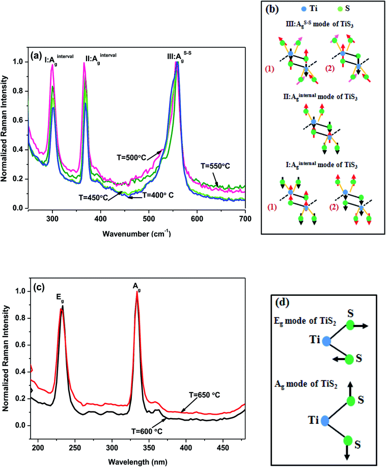
Raman spectroscopy is yet another excellent tool for the characterization of bulk as well as nanostructured materials. It has been analysed by observing the characteristic modes of the fabricated structures. In the present study so as to cross verify the composition of fabricated Ti–S nanostructure Raman spectroscopy of all the fabricated Ti–S nanostructures has been carried out which is depicted in Fig. 6. From Raman spectra, the distinct features of Ti–S can be clearly visible in Fig. 6(a–d). In Fig. 6(a), the spectra reveal three distinct peaks at ∼300 cm−1, ∼370 cm−1 and ∼557 cm−1 corresponding to Ag-type modes, indicating TiS3 structure of the Ti–S nanostructures. In this Raman spectra, the two peak corresponds to ∼300 cm−1 and ∼370 cm−1 contribute vibration within each TiS3 layer are termed as vibrational modes20 shown by AInternalg in Fig. 6(a). A close observation of a particular vibrational mode which corresponds to 300 cm−1 depicts that the two different optical branches coincide each other. This means that I-AInternalg mode consists of two degenerate modes which may be clearly visible in Fig. 6(b). It is important to note that the significant difference between the two vibrational modes i.e. the lower frequency mode ‘I-AInternalg’ and the higher frequency ‘II-AInternalg’ is their relative vibration direction between Ti atoms, bridge S atoms and S–S pairs across the two prisms noticeable in Fig. 6(b). As in the previously stated mode i.e. ‘I-AInternalg, the other mode termed as ‘III-AInternalg’ also contribute vibration of atoms which makes the individual layers except three S vibrate in opposite directions with Ti atom in one prism but the other prism vibrates in a central symmetry with it. Contrary to the aforesaid two modes, there is a highest frequency peak corresponds to 557 cm−1 appears doubly degenerate with higher FWHM value (26.6 cm−1) in comparison to two AInternalg modes depicted in Fig. 6(a). It is important to note that the peaks corresponds to 557 cm−1 are predominantly found in-plane out of phase motion of S–S pair and out-of-plane motion of Ti bridging S atoms depicted in Fig. 6(c). Assuming the nature S–S pair vibration, this peak is termed as III-AS–Sg. From the figure, it may be clearly visible that the presence of two near degenerate Raman peaks resulting in higher value of full-width half-maximum (FWHM) (26.2 cm−1) in comparison to I-AInternalg (19.3 cm−1)and II-AInternalg (15.6 cm−1). Again, Raman spectra has also been obtained for the Ti–S nanostructures grown at 600 °C and 650 °C and is shown in Fig. 6(c) which further confirms the characteristic modes associated with it i.e. Eg and Ag peaks at ∼233 cm−1 and ∼332 cm−1 respectively. These two peaks corresponds to the vibrations modes of TiS2 as reported earlier.21 The main difference between Eg and Ag modes is in vibrational direction shown in Fig. 6(d). In Eg mode (corresponds to 233 cm−1), the two S–S vibrates laterally opposite directions to Ti whereas in Ag mode (corresponds to 333 cm−1), the two S–S vibrates vertically opposite directions to Ti.
Till now studies on SEM and TEM confirmed the formation of titanium sulphide nanostructures ranging from 400 °C to 650 °C. The TEM images reveals magnified image to show the insight morphology and the diffraction patterns. After the confirmation of types and the morphology of the fabricated nanostructures, the elemental quantification, crystal structures as well as composition of Ti–S nanostructures has also been confirmed using EDX, XRD and Raman studies. Now, in this section the discussion has been made on the optical properties of the fabricated Ti–S nanostructures. All the nanostructures were synthesised with the same experimental procedures except their different growth temperatures for 24 hours. Now, the question arises that out of these fabricated nanostructures which one may be best suited for application oriented work like sensors, photodetectors etc., these can also be judged by their optical properties. More specifically, the optical properties of the nanostructures can be judged by normalized absorbance and the presence of defects levels. To confirm the changes in the optical properties of theses nanostructures, UV-vis spectroscopy and photoluminescence spectroscopy were carried out for all the fabricated Ti–S nanostructures. In Fig. 7(a), UV-vis spectrum of the Ti–S nanostructures fabricated on growth temperature ranging from 400 °C to 650 °C has been plotted. The absorbance spectrum of all the fabricated nanostructures is shown in Fig. 7(a). For all the fabricated Ti–S nanostructures (nanosheets, mixed phase nanosheets/nanoribbons, pure nanoribbons and nanodiscs), the absorbance spectrum has been taken in the visible region of electromagnetic spectrum so as to get difference in their optical properties. It may be noted from the figure that the normalized absorbance of the nanodiscs fabricated at growth temperature 650 °C is found to be highest. The normalized absorbance of the same nanodiscs fabricated at growth temperature 600 °C is found to be lower than those fabricated at growth temperature 650 °C. The normalized absorbance for nanosheets fabricated at growth temperature 400 °C is found to be lowest which lies just below the normalized absorbance for mixed phase nanosheets/nanoribbons fabricated on growth temperature 450 °C. At the same time, if we see the normalized absorbance for pure nanoribbons fabricated at growth temperature 500 °C and 550 °C, it is found to be higher than the mixed phase nanosheets/nanoribbons. Thus, it may be investigated from UV-vis spectra that comparatively better optical absorbance exist in Ti–S nanodiscs than the other three Ti–S nanostructures. Similarly, the defects levels and the surface to volume ratio of the nanostructures are found to be the favourable properties for sensing characteristics. This is because of the fact that more the defects levels, higher would be the surface to volume ratio which increases the exposure of the analyte molecules to the sensing surface resulting in the improvement of the sensing characteristics. To investigate the amount of defects levels, photoluminescence intensity (PLI) spectrum has been obtained which is plotted in Fig. 7(b). It may be noticeable from the figure that peak PLI is highest for nanodiscs fabricated at growth temperature 650 °C and lowest for the nanosheets fabricated at growth temperature 400 °C. All the other nanostructures lie in between the two in the same patterns as in the case of UV-vis absorbance spectrum. Hence, results of photoluminescence spectrum are found to be in agreement with the results predicted from UV-vis spectrum (Fig. 7(a)). Therefore, it may be expected that nanodiscs of Ti–S shows better sensing characteristics if used as sensing layer for particular analyte in comparison to other fabricated Ti–S nanostructures for the same analyte.
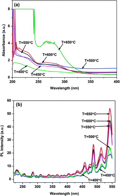 | ||
| Fig. 7 (a) UV-vis spectra (b) photoluminescence spectra of the titanium sulphide nanostructures grown at different temperature for 24 h. | ||
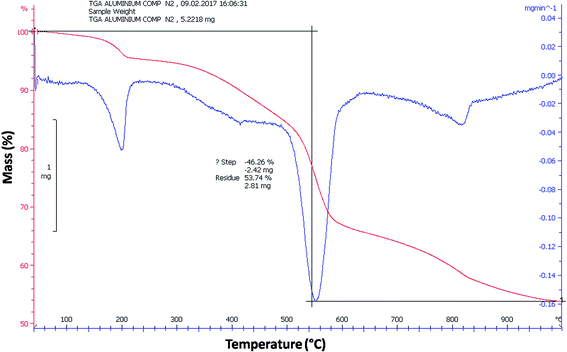
Further, the reason of formation of different Ti–S nanostructures at different growth temperatures can be explained using thermogravimetric analysis (TGA) and differential thermal analysis (DTA).In fact TGA/DTA measures the amount of mass change of certain material, either as a function of increasing temperature, or isothermally as a function of time. The measurements of TGA/DTA can be carried out in any of the atmosphere such as nitrogen, helium, ambient (air) or may be in vacuum. Generally, the measurements may be carried out routinely in the temperature range from 25 °C to 1000 °C. As shown in Fig. 8, TGA/DTA experiments were performed on the fabricated Ti–S nanostructures in vacuum in the varying temperature range from 25 °C to 1000 °C. In Fig. 8, the mass percentage of the TiS3 nanostructures was plotted as a function of temperature (TGA) and time (DTA). The red curve shows the TGA curve while the blue curve shows the DTA curve. It can be noticeable from Fig. 8 that initially when the temperature increases from 25 °C to 300 °C, a narrow dip is observed in the TGA curve (red) showing a slow decomposition of the TiS3. This decomposition is small enough and could not be able to change the composition of TiS3 instead it remains same as TiS3. On further increasing the temperature from 300 °C to 1000 °C, a sharp dip is observed nearly at 600 °C showing the strong decomposition of TiS3. At this temperature, the decomposition is strong enough to change the composition of TiS3 to TiS2. This finding is found to be in accordance with the SEM, XRD, RAMAN and TEM results. The DTA (blue) curve shows the similar trend as that of TGA (red) curve. To cross check the decomposition reaction of TiS3 DTA curve (blue) has been obtained. In DTA curve, as the time increases from 0 to 30 min, a small dip is observed at 15 min showing a slow decomposition of TiS3 nanostructures but the composition remains same as TiS3. On further increasing the time from 30 min to 100 min, a sharp dip is observed at nearly 50 min showing the strong decomposition of TiS3 to TiS2.
In this method of fabrication, the formation of TiS3 and TiS2 nanostructures can be interpreted completely using thermodynamics on the basis of TGA/DTA findings. The interpretation may be explained according to the findings of TGA/DTA along with XRD, SEM, and TEM/SAED. In Fig. 9, the schematic drawing of the formation of TiS3 and TiS2 nanostructures has been given in detail and the process has been divided into two steps. In the first step, the formation of TiS3 using mixture of sulphur (S8) and titanium (Ti) by chemical vapour transport reactions has been explained in detail. In typical CVT, as soon as thermal energy is provided in sealed ampoule where the mixture of S8 and Ti is present, the chemical bond of S8 breaks and sulphur atoms takes the position in the Ti lattice. The position of S in the Ti lattice is found to be such that TiS3 crystal takes the shape of prism where Ti is surrounded by three S atoms clearly shown in Fig. 9. Here it is noticeable that thermal energy is proportional to the growth temperature therefore the process of breaking of bonds of S8 and the formation of TiS3 occurs only upto certain growth temperature which is found to be from 400 °C to 550 °C. On further increasing the growth temperature i.e. from 600 °C to 650 °C, the obtained TiS3 starts decomposing into TiS2 by creating sulphur vacancy in TiS3 which has been displayed well in Fig. 9. It is found to be in consistent with the TGA/DTA results. Again, formation of TiS3 nanoribbons and TiS2 hexagonal nanodiscs can be explained using the growth orientations. The reasons of spatial confinement, the growth along one directions, for instance, [001], is found to be much faster than along the other directions consequently a nanoribbons has been formed which is clearly visible in Fig. 2(c and d). Similarly the growth along the other two crystallographically equivalent directions, [10–1] and [102], leads to form the branches on both sides. Further, as the growth continues, each side branches continue to grow and the formation of hexagonal nanodiscs occurs which is depicted from the SEM images in Fig. 2(e and f). Further, the prolonged reaction at particular temperature (say) 600 °C to 650 °C at 24 h, TiS2 nanodiscs seem to become stronger. Similarly, with prolonged reaction at growth temperature (say) 400 °C to 550 °C, the formation of TiS3 nanoribbons seem to become stronger and on increasing the growth temperature, TiS3 starts decomposing to accelerate the growth of TiS2 nanodiscs.
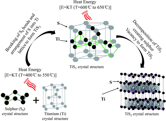 | ||
| Fig. 9 Pictorial representation showing the reason of formation of titanium trisulphide to disulphide on varying growth temperature from 400 °C to 650 °C. | ||
4. Conclusions
In conclusion, we developed two dimensional (2D) Ti–S nanostructures by chemical vapour transport (CVT) method and studied the growth temperature dependence of their structural/morphological, thermal and optical characteristics. The CVT reactions were performed keeping Ti![[thin space (1/6-em)]](https://www.rsc.org/images/entities/char_2009.gif) :
:![[thin space (1/6-em)]](https://www.rsc.org/images/entities/char_2009.gif) S equal to 1
S equal to 1![[thin space (1/6-em)]](https://www.rsc.org/images/entities/char_2009.gif) :
:![[thin space (1/6-em)]](https://www.rsc.org/images/entities/char_2009.gif) 3 varying the growth temperature ranging from 400 °C to 650 °C. The results suggests that keeping Ti
3 varying the growth temperature ranging from 400 °C to 650 °C. The results suggests that keeping Ti![[thin space (1/6-em)]](https://www.rsc.org/images/entities/char_2009.gif) :
:![[thin space (1/6-em)]](https://www.rsc.org/images/entities/char_2009.gif) S equal to 1
S equal to 1![[thin space (1/6-em)]](https://www.rsc.org/images/entities/char_2009.gif) :
:![[thin space (1/6-em)]](https://www.rsc.org/images/entities/char_2009.gif) 3, with an increase in growth temperature from 400 °C to 650 °C, a gradual change from nanosheets, mixed phase nanosheets/nanoribbons, nanoribbons of TiS3 to the nanodiscs of TiS2 occurs. The XRD, EDX and Raman studies confirms the formation of both TiS3 and TiS2. SEM as well as TEM/SAED results suggest that the techniques permit control of phase, crystal structure and morphology. At the same time, it is possible to follow the growth of Ti–S nanostructures from nanosheets, mixed phase nanosheets/nanoribbons of TiS3, pure phase nanoribbons of TiS3 to pure phase nanodiscs of TiS2. The results also suggest that all the growth temperature from 400 °C to 650 °C found to be suitable to obtain better crystallinity and good optical properties of the Ti–S nanostructures. Therefore, it is concluded that composition ratio of Ti and S as well as the growth temperature in CVT method both plays a crucial role in the formation of 2D Ti–S nanostructure of different shapes. Finally, the phenomenon of decomposition of titanium sulphide at elevated temperature has been explained using thermogravimetric analysis (TGA), differential thermal analysis (DTA) along with their pictorial representations.
3, with an increase in growth temperature from 400 °C to 650 °C, a gradual change from nanosheets, mixed phase nanosheets/nanoribbons, nanoribbons of TiS3 to the nanodiscs of TiS2 occurs. The XRD, EDX and Raman studies confirms the formation of both TiS3 and TiS2. SEM as well as TEM/SAED results suggest that the techniques permit control of phase, crystal structure and morphology. At the same time, it is possible to follow the growth of Ti–S nanostructures from nanosheets, mixed phase nanosheets/nanoribbons of TiS3, pure phase nanoribbons of TiS3 to pure phase nanodiscs of TiS2. The results also suggest that all the growth temperature from 400 °C to 650 °C found to be suitable to obtain better crystallinity and good optical properties of the Ti–S nanostructures. Therefore, it is concluded that composition ratio of Ti and S as well as the growth temperature in CVT method both plays a crucial role in the formation of 2D Ti–S nanostructure of different shapes. Finally, the phenomenon of decomposition of titanium sulphide at elevated temperature has been explained using thermogravimetric analysis (TGA), differential thermal analysis (DTA) along with their pictorial representations.
Conflicts of interest
There are no conflicts to declare.Acknowledgements
We greatly appreciate the financial support from Department of Science and Technology (DST), project no. ECR/2017/000530 India.References
- R. R. Chianelli, J. C. Scanlon, M. S. Whittingham and F. R. Gamble, Inorg. Chem., 1975, 14, 1691–1696 CrossRef CAS.
- G. Scholz, P. Joensen, J. M. Reyes and R. F. Frindt, Physica B+C, 1981, 105, 214–217 CrossRef CAS.
- J. Dahn and R. Haering, Mater. Res. Bull., 1979, 14, 1259–1262 CrossRef CAS.
- M. Remskar, A. Popovic and H. I. Starnberg, Surf. Sci., 1999, 430, 199–205 CrossRef CAS.
- M. Inoue and H. Negishi, J. Phys. Soc. Jpn., 1984, 53, 943–946 CrossRef CAS.
- H. E. Brauer, H. I. Starnberg, L. J. Holleboom, H. P. Hughes and V. N. Strocov, J. Phys.: Condens. Matter, 1999, 11, 8957–8973 CrossRef CAS.
- Y. Tison, H. Martinez, I. Baraille, M. Loudet and D. Gonbeau, Chem. Phys., 2003, 290, 267–278 CrossRef CAS.
- E. W. Ong, M. J. McKelvy, G. Ouvrard and W. S. Glaunsinger, Chem. Mater., 1992, 4, 14–17 CrossRef CAS.
- J. Chen, S. Li, Z. L. Tao and Y. T. Shen, J. Am. Chem. Soc., 2003, 125, 5284–5285 CrossRef CAS PubMed.
- J. Chen, Z. L. Tho and S. L. Li, Angew. Chem., Int. Ed., 2003, 42, 2147–2151 CrossRef CAS PubMed.
- H. G. Grimmeis, A. Rabenau, H. Hann and P. Z. Neiss, Elecktrochem, 1961, 65, 776–783 Search PubMed.
- I. J. Ferrer, J. R. Ares, J. M. Clamagirand, M. Barawi and C. Sánchez, Thin Solid Films, 2012, 535, 398–401 CrossRef.
- H. Haraldsen, E. Rost, A. Kjekshus and A. Steffens, Acta Chem. Scand., 1963, 17, 1283–1292 CrossRef.
- L. Brattas and A. Kjekshus, Acta Chem. Scand., 1972, 26, 3441–3449 CrossRef CAS.
- S. Kikkawa, M. Koizumi, S. Yamanaka, Y. Onuki and S. Tanuma, Phys. Status Solidi A, 1980, 61, K55–K57 CrossRef CAS.
- E. Finkman and B. Fisher, Solid State Commun., 1984, 50, 25–28 CrossRef CAS.
- I. J. Ferrer, M. D. Maciá, V. Carcelén, J. R. Ares and C. Sánchez, Energy Procedia, 2012, 22, 48–52 CrossRef CAS.
- J. O. Island, M. Buscema, M. Barawi, J. M. Clamagirand, J. R. Ares, C. Sánchez, I. J. Ferrer, G. A. Steele, H. Zant and A. C. Gomez, Adv. Opt. Mater., 2014, 2, 641–645 CrossRef CAS.
- F. Lévy and H. Berger, J. Cryst. Growth, 1983, 61, 61–68 CrossRef.
- L. Brattas and A. Kjekshus, Acta Chem. Scand., 1972, 2, 3441–3449 CrossRef.
- S. Furuseth, L. Brattås and A. Kjekshus, Acta Chem. Scand., Ser. A, 1975, 29, 623–631 CrossRef.
- J. Dai, M. Li and X. C. Zeng, WIREs Comput. Mol. Sci., 2016, 6, 211–222 CrossRef CAS.
- J. O. Island, M. Barawi, R. Biele, A. Almazán, J. M. Clamagirand, J. R. Ares, C. Sánchez, H. Zant, J. V. Álvarez, R. D. Agosta, I. J. Ferrer and A. C. Gomez, Adv. Mater., 2015, 27, 2595–2601 CrossRef CAS PubMed.
- J. Dai and X. C. Zeng, Angew. Chem., Int. Ed., 2015, 54, 7572–7576 CrossRef CAS PubMed.
- S. Zaitsev-Zotov, Microelectron. Eng., 2003, 69, 549–554 CrossRef CAS.
- J. J. Ma, X. Y. Liu, X. J. Cao, S. H. Feng and M. E. Fleet, Eur. J. Inorg. Chem., 2006, 3, 519–522 CrossRef.
- X. C. Wu, Y. R. Tao and Q. X. Gao, Nano Res., 2009, 2, 558–564 CrossRef CAS.
- J. Chen, S. L. Li, Z. L. Tao and F. Gao, Chem. Commun., 2003, 8, 980–981 RSC.
- S. Prabakar, C. W. Bumby and R. D. Tilley, Chem. Mater., 2009, 21, 1725–1730 CrossRef CAS.
- Y. Zhang, Z. K. Li, H. B. Jia, X. H. Luo, J. Xu, X. H. Zhang and D. P. Yu, J. Cryst. Growth, 2006, 293, 124–127 CrossRef CAS.
- H. S. Chang and D. M. Schleich, J. Solid State Chem., 1992, 100, 62–70 CrossRef CAS.
- S. J. Denholme, J. B. Gallagher, P. Dobson, J. M. R. Weaver and D. H. Gregory, Isr. J. Chem., 2010, 50, 515–523 CrossRef CAS.
- K. Wu1, et al., Nat. Commun., 7, 12952 Search PubMed.
- D. Y. Oh, Y. E. Choi, D. H. Kim, Y. G. Lee, B. S. Kim, J. Park, H. Sohn and Y. S. Jung, J. Mater. Chem. A, 2016, 4, 10329–10335 RSC.
- Z. Yang, J. Lu, D. Bian, W. Zhang, X. Yang, J. Xia, G. Chen, H. Gu and G. Ma, J. Power Sources, 2014, 272, 144–151 CrossRef CAS.
- F. Tronc and M. Huber, C.R. hebd. Seanc., Acad. Sci. Paris Ser. C., 1969, 268, 1771 Search PubMed.
| This journal is © The Royal Society of Chemistry 2019 |

