 Open Access Article
Effect of oxygen vacancy concentration on indium tungsten oxide UV-A photodetector
Kuan-Yin Chena,
Sheng-Po Chang *a and
Chih-hung Linb
aInstitute of Microelectronics and Department of Electrical Engineering, Advanced Optoelectronic Technology Center, National Cheng Kung University, Tainan 70101, Taiwan. E-mail: changsp@mail.ncku.edu.tw
bNational Nano Device Laboratories, Tainan 741, Taiwan
First published on 20th December 2018
Abstract
An indium tungsten oxide (IWO) ultraviolet (UV) photodetector was fabricated with radio frequency magnetron sputtering. IWO thin films were deposited on devices under various oxygen partial pressure ambiences. With higher oxygen flow ratio, the oxygen vacancies were filled up, reducing the carrier concentration. Lowering the number of defects, such as oxygen vacancies, was effective for optimizing device performance. The on–off current ratio of an IWO UV-A photodetector at 10% oxygen partial pressure could reach 4.56 × 10⁴, with a photoresponsivity of 1.9 × 10⁻² A W−1, as well as a rejection ratio of 2.68 × 10⁴ at a voltage bias of 10 V.
Introduction
Owing to various current and potential developments in the military, intersatellite communications, astronomical technology, medical observation, and environmental security, ultraviolet (UV) photodetectors are increasingly drawing the attention of scientists and industries.1–3 The advantages of UV photodetectors are their simple fabrication processes, rapid response speed, low dark currents, and good compatibility with integrated circuits. Nevertheless, the band gap of Si is so narrow that it is essential to find some materials having larger band gaps, for application on photodetectors. III-Nitride materials such as AlGaN have been reported as potential candidates for applications of photodetectors.4 In2O3-based amorphous oxide materials, such as In2O3, InSiO, InTiO, Sn–InZnO, Hf-InZnO, InGaZnO (IGZO), and indium tungsten oxide (IWO), can be fabricated using a low-cost process, because of their low temperature requirement. Owing to their high mobility and optical transparency, these materials are desirable candidates as the channel layers for thin-film transistors (TFTs). The a-IGZO TFT is considered the most promising semiconductor material for advanced displays in the future. However, a-IGZO consists of Ga2O3 and ZnO, which limits the wet-etching process for the preparation process of a-IGZO TFTs, because the Ga-containing semiconductor is sensitive to acid, and the Zn-containing semiconductor is sensitive to acid and moisture in the atmosphere.5,6 In addition, ZnO-based TFTs fabricated with a low-temperature process are difficult to operate stably.7 Therefore, finding Ga-free or Zn-free amorphous oxide thin films is essential. Studies on IWO applied on photodetectors are rare in recent research. The band gap of In2O3 is close to the visible blind region, and the band gap energy is approximately 2.9 eV. Doping W into In2O3 can help increase the band gap energy to approximately 3.8 eV. Moreover, the W element has the characteristics of a carrier suppressor, which can replace Zn or Ga elements, making the devices much more stable.8 In this study, IWO UV photodetectors were investigated under different oxygen partial pressures, using a radio frequency (RF) magnetron sputtering system, and annealed under various temperature ambiances in air. The detailed performance and response of the devices are discussed in the following sections.Experimental
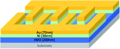
In this work, an IWO photodetector was investigated using the following process. The structure of the device is shown in Fig. 1. Firstly, quartz substrates were sequentially cleaned using acetone, isopropyl alcohol, and deionized water placed in ultrasonic oscillators, for 5 min. Thereafter, the substrates were dried with nitrogen. Secondly, an RF sputtering system was operated, and 200 nm IWO thin films were deposited on quartz substrates, using an IWO target (In2O3/WO3 = 96/4 wt%) at room temperature under different gas flow ratios. The gas flow ratios of O2/(Ar + O2) were 2%, 4%, 6%, and 10%, and the total gas flow was 50 sccm. The detailed ambiances during fabrication are listed below: for the 2% IWO thin film, it was a mixture of 49 sccm of Ar and 1 sccm of oxygen, for the 4% IWO thin film, it was a mixture of 48 sccm of Ar and 2 sccm of oxygen, for the 6% IWO thin film, it was a mixture of 47 sccm of Ar and 3 sccm of oxygen, and for the 10% IWO thin film, it was a mixture of 45 sccm of Ar and 5 sccm of oxygen. Before the deposition process, the sputtering chamber was pumped down under a pressure of 5 × 10⁻⁶ torr. The RF power was 80 W, and the rotation speed was 15 rpm. Thirdly, via an interdigital shadow mask, Ni/Au (30/70 nm) metal contact electrodes were deposited on substrates by thermal evaporation. The fingers of the shadow masks were 1.2 mm in length and 0.1 mm in width, with a 0.2 mm interfinger distance. Finally, the current–voltage (I–V) characteristics of the UV photodetectors were measured using a semiconductor parameter analyzer (Agilent B1500A). The response of the photodetector was measured with a 250 W Xe lamp equipped with a monochromator, as the light source.Results and discussion
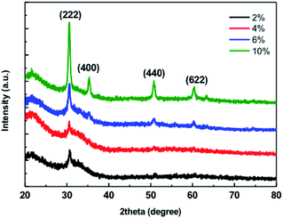
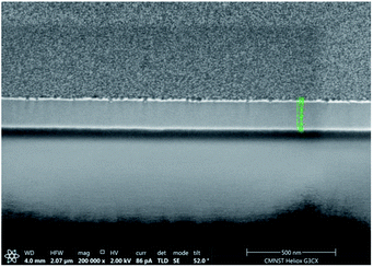
The X-ray diffraction (XRD) spectra of the IWO thin-film samples are shown in Fig. 2. It is obvious that all the diffraction peaks—(222), (400), (440), and (622)—correspond to the cubic phase of bixbyite-type In2O3, and they can be easily identified. In addition, there is no peak relevant to other crystalline structures. This implies that tungsten, which was doped into the In2O3 films, did not change the structure of the films. Furthermore, the peak intensity increased as the oxygen flow ratio increased. The roughness profiles of the IWO films, obtained using atomic force microscopy (AFM), are shown in Fig. 3. The root mean square (RMS) roughness of the 2%, 4%, 6%, and 10% IWO thin films were 1.800, 1.807, 1.865, and 1.897 nm, respectively. As the oxygen flow ratio increased, the RMS roughness of the films increased. When the oxygen partial pressure increased, more oxygen ions entered the films, increasing the RMS roughness. The image shows that the thickness of the film was 200 nm, and it was deposited with good uniformity, by the RF sputtering system.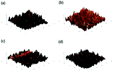 | ||
| Fig. 3 Roughness profiles of IWO films, obtained using AFM, for oxygen partial pressures of (a) 2%, (b) 4%, (c) 6%, and (d) 10%. | ||
To confirm whether the thickness of the IWO thin films is correct, a cross-section photo was taken using scanning electron microscopy (SEM), and is displayed in Fig. 4.
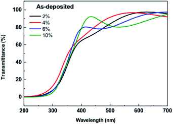
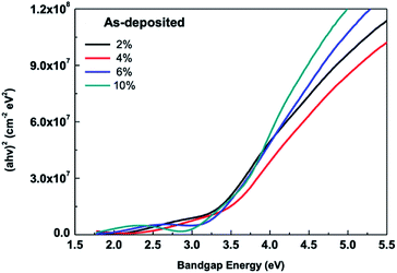
The optical transmittance spectra of the IWO films are shown in Fig. 5. The characteristic curves show that the transmittance was more than 80% in the visible region, which implies that the IWO thin films exhibited good selectivity for UV light, which is an important characteristic for UV photodetectors. Fig. 6 displays the absorption coefficient spectra of the IWO films. The plot of the squared absorption coefficient versus photon energy was used to determine the values of the band gap. By calculating the slope of the linear curve and making an intersection between the tangent line as well as the horizontal axis, the band gaps of IWO were found to be approximately 3.13 to 3.39 eV. The band gaps of the IWO films for less than 2%, 4%, 6%, and 10% oxygen flow were 3.12, 3.28, 3.32, and 3.38 eV. The band gap of IWO shows that strong absorption for photons occurs at a wavelength shorter than 400 nm.
IWO UV photodetectors on quartz substrates, investigated using RF sputtering at room temperature, are discussed in this section. Fig. 7 shows the I–V characteristics of the IWO UV photodetectors, for various oxygen flow ratios. The on–off current ratios of the 2%, 4%, 6%, and 10% IWO UV photodetectors were 5.37 × 10², 2.03 × 10⁴, 2.82 × 10⁴, and 4.56 × 10⁴, respectively, as displayed in Table 1.
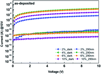 | ||
| Fig. 7 I–V characteristics of as-deposited IWO UV photodetectors, for various oxygen partial pressures. | ||
| (Vbias = 10 V) | 2% | 4% | 6% | 10% |
|---|---|---|---|---|
| Iphoto/Idark current ratio | 5.37 × 10² | 2.03 × 10⁴ | 2.82 × 10⁴ | 4.56 × 10⁴ |
| Photoresponsivity (A W−1) (@290 nm) | 4.32 × 10⁻³ | 9.46 × 10⁻² | 7.4 × 10⁻² | 1.9 × 10⁻² |
| Rejection ratio | 1.06 × 10³ | 8.54 × 10³ | 2.51 × 10⁴ | 2.68 × 10⁴ |
Fig. 8 displays the photoresponsivity spectra of the 2%, 4%, 6%, and 10% IWO UV photodetectors at a 10 V bias. These IWO UV photodetectors were exposed to light of a wavelength between 230 and 500 nm. The highest responsivity occurred at a wavelength of 290 nm, and Table 1 shows the values of photoresponsivity for different IWO UV photodetector processing conditions, at this wavelength position. The visible-to-UV rejection ratio of the IWO UV photodetectors in this work was defined as the ratio of the responsivity at a wavelength of 290 nm to that at a wavelength of 500 nm, which is represented as
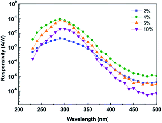 | ||
| Fig. 8 Photoresponsivity versus wavelength diagram of 2%, 4%, 6%, and 10% IWO UV photodetectors under a wavelength of 290 nm. | ||
The rejection ratios and cutoff wavelengths under various oxygen partial pressures, at a bias of 10 V, were calculated, and are listed in Table 1. The rejection ratios of the IWO UV photodetectors increased when the oxygen flow increased. However, the cutoff wavelengths were 310 to 320 nm for all the devices.
Fig. 9 shows the rise time and decay time of the IWO UV photodetectors at a voltage bias of 10 V. Before the measurements for testing the switching characteristics, the devices were all placed in a dark room for 30 min; this prevented the devices from being exposed to light. The devices were illuminated with 290 nm UV light for 150 s. When the current reached the saturation region, the light source was removed. Every 300 s, the steps were repeated. The 2%, 4%, 6%, and 10% devices were compared at the same scales and cycles. In this work, the definitions of rise time and fall time are the time for the devices to reach 10% and decay to 90% of the maximum illuminated current, respectively. The combination of oxygen vacancies produces subgap states, and this obstructs carrier excitation after the films are exposed to UV light. The diagrams show that with an increase in the oxygen partial pressure from 2% to 10% during fabrication, the devices became more stable, and the rise time, as well as the decay time, reduced during switching. Table 2 displays previous results of photodetectors fabricated with different materials and methods. The IWO material, as well as the method in this work, have more potential, in comparison with other applied UV photodetectors and methods.
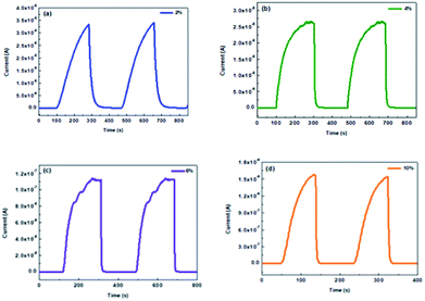 | ||
| Fig. 9 Time response of IWO UV photodetectors investigated under various oxygen partial pressures: (a) 2%, (b) 4%, (c) 6%, and (d) 10%. | ||
Conclusions
In summary, IWO UV photodetectors were investigated at various oxygen flow ratios, using an RF magnetron sputtering system. As the oxygen partial pressure increased, the number of oxygen vacancies was suppressed; this decreased the carrier concentration. Therefore, a 10% oxygen flow ratio is the optimized parameter for IWO UV photodetectors, with an on–off current ratio of 4.56 × 10⁴, photoresponsivity of 1.9 × 10⁻² A W−1, and rejection ratio of 2.68 × 10⁴ at a voltage bias of 10 V.Conflicts of interest
There are no conflicts to declare.Acknowledgements
This work was supported by the Ministry of Science and Technology [contract numbers MOST 106-2221-E-006-178 and MOST 107-2221-E-006-146]; the Center for Frontier Materials and Micro/Nano Science and Technology, National Cheng Kung University, Taiwan; and the Advanced Optoelectronic Technology Center, National Cheng Kung University, for projects from the Ministry of Education.References
- P. Bergonzo and R. B. Jackman, Diamond-based radiation and photon detectors, in Thin-Film Diamond II, ed. C. E. Nebel, J. Ristein, Elsevier, 2004, ch. 6, vol. 77, pp. 197–309 Search PubMed.
- E. Monroy, F. Omnès and F. Calle, Wide-bandgap semiconductor ultraviolet photodetectors, Semicond. Sci. Technol., 2003, 18, 33 CrossRef.
- N. Biyikli, O. Aytur, I. Kimukin, T. Tut and E. Ozbay, Solar-blind AlGaN-based Schottky photodiodes with low noise and high detectivity, Appl. Phys. Lett., 2002, 81, 3272–3274 CrossRef CAS.
- J. D. Brown, J. Li, P. Srinivasan, J. Matthews and J. F. Schetzina, Solar-Blind AlGaN Heterostructure Photodiodes, MRS Internet J. Nitride Semicond. Res., 2000, 5, 9 CrossRef.
- P. T. Liu, Y. T. Chou and L.-F. Teng, Environment-dependent metastability of passivation-free indium zinc oxide thin film transistor after gate bias stress, Appl. Phys. Lett., 2009, 95, 233504 CrossRef.
- S. Aikawa, P. Darmawan, K. Yanagisawa, T. Nabatame, Y. Abe and K. Tsukagoshi, Thin-film transistors fabricated by low-temperature process based on Ga- and Zn-free amorphous oxide semiconductor, Appl. Phys. Lett., 2013, 102, 102101 CrossRef.
- J. S. Park, K. Kim, Y. G. Park, Y. G. Mo, H. D. Kim and J. K. Jeong, Novel ZrInZnO Thin-film Transistor with Excellent Stability, Adv. Mater., 2009, 21, 329–333 CrossRef CAS.
- Z. Lu, F. Meng, Y. Cui, J. Shi, Z. Feng and Z. Liu, High quality of IWO films prepared at room temperature by reactive plasma deposition for photovoltaic devices, J. Phys. D: Appl. Phys., 2013, 46, 7 Search PubMed.
- T. H. Chang, S. J. Chang, W. Y. Weng, C. J. Chiu and C. Y. Wei, Amorphous Indium–Gallium–Oxide UV Photodetectors, IEEE Photonics Technol. Lett., 2015, 27, 2083–2086 CAS.
- Y. Kokubun, K. Miura, F. Endo and S. Nakagomi, Sol-gel prepared β-Ga2O3 thin films for ultraviolet photodetectors, Appl. Phys. Lett., 2007, 90, 031912 CrossRef.
- W. Y. Weng, T. J. Hsueh, S. J. Chang, G. J. Huang and S. C. Hung, Growth of Ga2O3 Nanowires and the Fabrication of Solar-Blind Photodetector, IEEE Trans. Nanotechnol., 2011, 10, 1047–1052 Search PubMed.
- L. Su, Y. Zhu, D. Yong, M. Chen, X. Ji, Y. Su, X. Gui, B. Pan, R. Xiang and Z. Tang, Wide range bandgap modulation based on ZnO-based alloys and fabrication of solar blind UV detectors with high rejection ratio, ACS Appl. Mater. Interfaces, 2014, 6, 14152–14158 CrossRef CAS PubMed.
- L. Wang, Z. Ju, C. Shan, J. Zheng, D. Shen, B. Yao, D. Zhao, Z. Zhang, B. Li and J. Zhang, MgZnO metal–semiconductor–metal structured solar-blind photodetector with fast response, Solid State Commun., 2009, 149, 2021–2023 CrossRef CAS.
| This journal is © The Royal Society of Chemistry 2019 |

