 Open Access Article
Room-temperature synthesized SnO2 electron transport layers for efficient perovskite solar cells†
Shengwei Shia,
Jing Lia,
Tongle Bua,
Shili Yanga,
Junyan Xiaob,
Yong Peng a,
Wei Lia,
Jie Zhong
 a,
Zhiliang Ku
 a,
Yi-Bing Chengacd and
Fuzhi Huang
 *a
*a
aState Key Laboratory of Advanced Technology for Materials Synthesis and Processing, Wuhan University of Technology, Wuhan 430070, PR China. E-mail: fuzhi.huang@whut.edu.cn
bSchool of Materials Science and Engineering, Wuhan University of Technology, Wuhan 430070, PR China
cDepartment of Materials Science and Engineering, Monash University, VIC 3800, Australia
dARC Centre of Excellence in Exciton Science, Monash University, VIC 3800, Australia
First published on 29th March 2019
Abstract
Tin oxide (SnO2) is widely used as electron transport layer (ETL) material in perovskite solar cells (PSCs). Numerous synthesis methods for SnO2 have been reported, but they all require a proper thermal treatment for the SnO2 ETLs. Herein we present a simple method to synthesize SnO2 nanoparticles (NPs) at room temperature. By using butyl acetate as a precipitator and a proper UV–Ozone treatment to remove Cl residuals, excellent SnO2 ETLs were obtained without any thermal annealing. The highest power conversion efficiency (PCE) of the prepared PSCs was 19.22% for reverse scan (RS) and 18.79% for forward scan (FS). Furthermore, flexible PSCs were fabricated with high PCEs of 15.27%/14.74% (RS/FS). The low energy consuming SnO2 ETLs therefore show great promise for the flexible PSCs' commercialization.
Introduction
Recently, hybrid organic–inorganic metal halide perovskites have been regarded as prospective materials in the photovoltaic field due to their outstanding photovoltaic properties, ease of fabrication, moderate band gap, etc.1–4 Perovskite solar cells which employ perovskites as light absorption layers have developed rapidly since they were first reported in 2009.5 The PCE of PSCs grew up from 3.8 to 23.7% in less than 10 years.5–11 The typical device includes a transparent conductive layer, an electron transport layer (ETL), a light absorption layer (perovskite), a hole transport layer and a back electrode. Since Snaith et al. first reported a planar heterojunction PSC in 2013,12 it has received more and more attention due to its simpler structure compared to the mesoporous structure. This makes it possible to involve low temperature processed ETLs. Many kinds of n-type semiconductors can be used as ETLs.13–17 Among the candidates, SnO2 exhibits salient features, such as wide optical band gap (3.6–4.0 eV), good transparency, high mobility up to 240 cm2 V−1 s−1, excellent chemical stability, and easy low-temperature preparation.18–20 There have been many reported processes for preparing SnO2 ETLs, embracing spin-coating,21–26 slot die coating,27 atomic layer deposition,28,29 chemical bath deposition,30,31 sol–gel method,32–34 etc. Besides, all methods above require a proper temperature treatment in the fabrication process or post-treatment, and sometimes even involve a high temperature annealing. High temperature processes not only cost extra energy, but also restrain the use of flexible plastic substrates (such as PET-ITO).35,36 It is of no doubt that a low temperature process is vital for the commercialization of flexible PSCs.SnO2 NPs have been synthesized via a low temperature process by ultrasonic-assisting37 or introducing thiourea as an additive in precursor.38 However, they still cannot avoid a proper annealing treatment for the prepared SnO2 film to remove the additive and induce good connections between nanoparticles. Herein we develop a simple sol–gel method to prepare uniform SnO2 NPs at room temperature. Furthermore, the prepared SnO2 ETLs work well without any thermal annealing. The PSCs made with annealing-free SnO2 ETLs achieved a high PCE of 19.22% by using a mixed cation perovskite absorber39 (KCsFAMAPbIxBr3−x, where FA: formamidine, MA: methylamine). In addition, the corresponding flexible PCSs obtained a PCE of 15.27%. The SnO2 NPs via such a simple thermal-free process allow them to be a promising ETL material in the potential commercial application.
Results and discussion
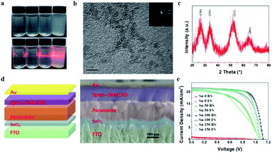
In order to synthesize SnO2 NPs, anhydrous SnCl4 was dissolved in deionized water under the circumstance of ice water bath. The concentration of SnCl4 solution was 0.01 M, 0.03 M, 0.05 M, 0.075 M, and 0.1 M, respectively. All solutions were kept under room temperature. The solution became translucent in varying degrees with time. 0.01 M, 0.03 M and 0.05 M solutions turned into semi-transparent after 20 min, 60 min and 100 min, respectively. Whereas 0.075 M and 0.1 M solutions took a much longer time (more than 400 min and 28 hours, respectively) to reach this state. The change of the different SnCl4 solutions with time is shown in Fig. S1.† This demonstrates that the kinetic process of the hydrolysis of SnCl4 can be regulated by different concentrations of SnCl4 aqueous solution. To further study the kinetics of the hydrolysis, the 0.05 M SnCl4 solution was characterized with time break of 0 min, 50 min, 100 min and 150 min, labelled Sn-0, Sn-50, Sn-100 and Sn-150, respectively. Fig. 1a shows that the Sn-0 is transparent while the Sn-100 is translucent. However, the Sn-150 is nearly opaque. A Tyndall effect can be observed when a laser beam goes through the solution (Fig. 1a). With the time increases, the Tyndall effect becomes clearer. However, the Sn-150 contains too many colloids. Thus, the Sn-100 is chosen for the late use. The Raman spectra of the Sn-0 to Sn-150 indicate the presence of SnO2 NPs (Fig. S2a†). The peak of ∼478 cm−1 belongs to the SnO2 Eg Raman active optical modes. The Raman spectra also prove the amount of SnO2 NPs accumulating with the hydrolysis time.To collect SnO2 NPs, isopropanol (IPA) was used as a precipitator. After washing, the SnO2 NPs were finally dispersed in ethanol. Transmission electron microscopy (TEM) was employed to examine the structure of the SnO2 NPs. Fig. 1b shows the typical TEM image of the Sn-100 derived SnO2 NPs with grain sizes below 5 nm. The polycrystalline feature of the Sn-100 was revealed by the electron diffraction rings (Fig. 1b inset). In addition, the corresponding X-ray diffraction (XRD) spectrum of Sn-100 (Fig. 1c) further confirms the presence of the SnO2 nanocrystals. The XRD spectra of Sn-0, Sn-50, Sn-100 and Sn-150 NPs are shown in Fig. S2b,† indicating that the crystallinity increases with the hydrolysis time.
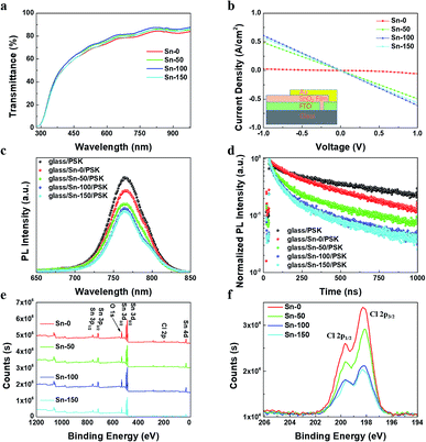
To fabricate ETLs, the Sn-0, Sn-50, Sn-100, Sn-150 NPs were spun coating onto FTO glass respectively. All the ETLs dried at room temperature without annealing. Then the perovskite film and spiro-OMeTAD film were sequentially deposited by spin coating. Finally, gold was deposited onto the spiro-OMeTAD layer as a back electrode. The cross-sectional SEM image of the device structure is shown in Fig. 1d. Fig. 1e shows the J–V curves of the PSCs, the corresponding photovoltaic characteristics are listed in Table 1, and the distribution of the characteristics is shown in Fig. S2c.† The Sn-100 has an excellent performance with an average PCE 17.87% for reverse scan (RS), while the Sn-0 has a very poor average PCE of 0.32% (RS). It is found that the longer hydrolysis time promotes the higher short-circuit current density (Jsc) output. However, if the hydrolysis time goes over 150 min, the Jsc starts to decrease. To find out the cause, the transmittance of SnO2 ETLs were firstly tested by Ultraviolet-visible spectroscopy (UV-Vis) (Fig. 2a). Although the Sn-100 ETL shows a little higher transmittance than Sn-0, the big difference in Jsc should not be ascribed to it. The electrical conductivity of the ETLs (Fig. 2b) was then measured. The conductivity of the Sn-0 film is extremely poor, which is possibly due to too much SnCl4 residual in the film. The poor conductivity resulted in the low current and fill factor. The Sn-100 ETL has the highest transmittance and conductivity among these ETLs. Therefore, the Sn-100 device has the highest PCE. To find out how the charge extraction property at the SnO2 ETLs/perovskite interface, the steady photoluminescence (PL) and time-resolved photoluminescence (TRPL) measurements were performed. The PL spectra (Fig. 2c) indicate longer hydrolysis time induced a better charge extraction ability of the prepared SnO2 ETLs, which is further confirmed by the TRPL spectra (Fig. 2d). It should be pointed out that Sn-100 and Sn-150 show quite similar PL properties. Further study of SnO2 ETLs about Cl element remnants was carried out by X-ray photoelectron spectroscopy (XPS) as shown in Fig. 2e. The spectra clearly indicate the presence of SnO2. Furthermore, it could be found that with the longer reaction time, less Cl residues in the ETLs as Sn-100 and Sn-150 films have a much lower Cl 2p peak (2p spin-orbital split p3/2 and p1/2 (ref. 40)) intensity. The residual Cl− on the surface leads to partial decomposition of perovskite.26 The XRD of the perovskites validates the PbI2 existence (Fig. S2d†). Compared to the perovskite films prepared on FTO directly and SnO2 ETLs, the major distinction is the residue of PbI2, weaker peak intensity of PbI2 for perovskite film on FTO. The scan electron microscope (SEM) images show the SnO2 films and perovskite films (Fig. S3a–h†) morphologies and microstructures. The SnO2 film prepared by the Sn-0 NPs have pinholes, the Sn-50 film has reduced and smaller pinholes, and both Sn-100 and Sn-150 films show perfect morphologies without pinholes. All the films comprise compact large perovskite grains, in spite of the existence of the light coloured PbI2 grains.
| 25 °C | J–V sweep direction | Voc (V) | Jsc (mA cm−2) | FF | PCE (%) | Rs (Ω cm2) | Rsh (kΩ cm2) |
|---|---|---|---|---|---|---|---|
| 0 min (Sn-0) | RS | 1.057 | 1.09 | 0.28 | 0.32 | 744.6 | 0.4 |
| FS | 1.072 | 0.76 | 0.23 | 0.19 | 506.0 | 0.4 | |
| 50 min (Sn-50) | RS | 1.070 | 20.51 | 0.54 | 11.85 | 16.3 | 1.0 |
| FS | 1.066 | 20.37 | 0.50 | 10.85 | 15.8 | 10.8 | |
| 100 min (Sn-100) | RS | 1.119 | 21.58 | 0.74 | 17.87 | 5.6 | 0.7 |
| FS | 1.118 | 21.73 | 0.64 | 15.53 | 7.8 | 17.0 | |
| 150 min (Sn-150) | RS | 1.081 | 20.98 | 0.72 | 16.33 | 6.9 | 9.3 |
| FS | 1.071 | 20.92 | 0.62 | 13.89 | 10.3 | 1.8 |
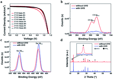
The J–V characteristics show there is still hysteresis of PSCs. It has been reported that the UV–Ozone (UVO) treatment for SnO2 film can effectively reduce the hysteresis.41 The Sn-100 NPs films were then treated with the UVO by different times, from 5 min, 10 min and 15 min, respectively. Table S1† and Fig. 3a show the parameters as well as the J–V curves of the treated PSCs. Apparently, all the treated devices have depressed hysteresis to less than 1% and the Jsc rises universally. XPS spectra of Cl 2p spin–orbit (Fig. 3b) show that the peaks related to Cl 2p p3/2 and p1/2 disappear after the UVO treatment, indicating the removal of the Cl residues in the film. The Cl residues could be attributed to the residuary SnCl4 from the precursor. The presence of SnCl4 would decrease the conductivity of the prepared ETLs. By removing the SnCl4 residuals via the UVO, the conductivity of films could increase as showed in Fig. S4.† This in turn results in the increased conductivity. Furthermore, after the UVO treatment, the Sn 3d5/2 and Sn 3d3/2 binding energies move toward to 487.2 and 495.6 eV respectively (Fig. 3c), which are very closed to reported values of the SnO2.22 This means much purer SnO2 forms. Due to the less Cl remnants in the SnO2 ETLs, the less PbI2 forms in the perovskite films as shown in the XRD spectra (Fig. 3d), producing highly crystalline perovskite. SEM images (Fig. S5a–h†) show the morphologies of the UVO treated SnO2 and perovskite films. Both SnO2 and large grain perovskite films are quite compact. With the longer time treatment, less PbI2 grains are found in the perovskite films.
Although the Sn-100 devices have achieved a promising performance, the PCEs (17.97/17.26%, RS/FS) are not high enough compared to the reported thermal processed devices. Considering IPA can mix with water, little trace of water may remain in SnO2 NPs precursor solution. The trace of water will stay in the ETL and damage the interface of ETL/perovskite. So, a new precipitator which is immiscible with water and can be anti-solvent for perovskite is required to replace the IPA in order to improve the performance further. Previously, ethyl acetate has been employed as an effective anti-solvent for the perovskite.42 After investigation of methyl acetate (MA), ethyl acetate, propyl acetate and butyl acetate (BA), BA stands out due to its lower polarity, more hydrophobic, and less dosage as precipitator. Ethyl alcohol was used as intermediate solvent to allow ester to mix with water so that SnO2 NPs can precipitate. We used Sn-IPA and Sn-BA to distinguish IPA and BA as the precipitant to collect SnO2 NPs which were prepared from 100 min hydrolysis. All the films were treated with the UVO for 15 min. The Fig. S6a and b† show the PL and TRPL spectra of the perovskite/Sn-IPA and perovskite/Sn-BA. It could be found that the Sn-BA ETL could extract the electrons more efficiently than the Sn-IPA ETL. The J–V curves along with the photovoltaic characteristics of the champion PSCs based on the Sn-IPA and Sn-BA ETLs are showed in Fig. 4a. The champion PCEs of the Sn-BA based PSC are 19.22/18.79% (RS/FS), while the Sn-IPA based devices have the PCEs of 17.97/17.26% (RS/FS). The EQE spectra (Fig. 4b) indicate the Sn-BA based device has higher values across all the wavelengths, resulting in an integrated photocurrent of 22.30 mA cm−2 compared to 21.09 mA cm−2 of the Sn-IPA based device. The power steady state current output of Sn-BA is 20.23 mA cm−2 with PCE ∼ 18.53%, whereas Sn-IPA is 19.85 mA cm−2 at first but gradually declined to 18.26 mA cm−2 after 150 seconds as shown in Fig. 4c. To further test the stability, all devices were stored in ambient air without encapsulation. The PCE of the champion Sn-BA based device grew up 6.7% (from 18.02% to 19.22%) in first 80 h then attenuated slowly. The reason of the increase of the efficiency at the initial stage is still uncertain, possible due to the relaxation of the ions moving in the perovskites. Over 1500 hours, its PCE still remained about 91.8% compared to the original value. Extra devices were taken to conduct the test, showing the similar trends (Fig. S7†). For the Sn-IPA based device, it kept decaying gradually and remained 75.5% PCE after 1500 hours (Fig. 4d).
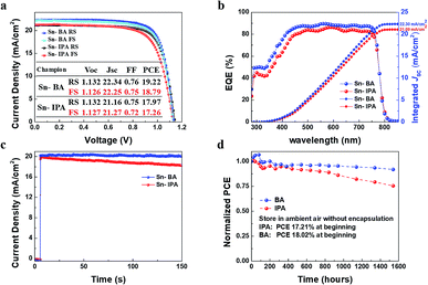 | ||
| Fig. 4 Performance of the Sn-BA and Sn-IPA champion PSCs. (a) J–V curves, (b) EQE spectra, (c) steady-state power output with the bias voltage of 0.93 V, and (d) stability test. | ||
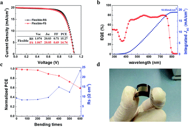
The above results have shown that an excellent process of room temperature synthesis SnO2 ETLs without annealing was developed. Then flexible PSCs were fabricated on the Sn-BA ETL/PET-ITO as showed in Fig. 5a–d. The highest PCE of the flexible PSCs is 15.27/14.74% (RS/FS) with the Jsc of 20.05 mA cm−2, close to the integrated photocurrent (18.95 mA cm−2) form the EQE spectrum (Fig. 5a and b). After bending 600 times, the PCE remained 59.26% compared to the original PCE due to the doubled Rs after so many times bending (Fig. 5c).
Conclusions
In brief, a simple strategy for synthesizing SnO2 NPs was proposed. Anhydrous SnCl4 was diluted to 0.05 M and hydrolyzed under room temperature. BA was used as a precipitator to collect SnO2 NPs. After spin coating them onto substrate, a UVO treatment was employed to clean Cl residual in order to reduce hysteresis. Such ETLs do not require any further thermal treatment. Finally, the highest PCE for rigid and flexible PSC of 19.22/18.79% and 15.27/14.74% (RS/FS) were achieved respectively. Our results demonstrated an energy-efficient process to prepare ETLs for PSCs, which is possible for further PSCs commercialization.Conflicts of interest
There are no conflicts to declare.Acknowledgements
This work is financially supported by the National Natural Science Foundation of China (NSFC 2187050787, 51672202) and the Technological Innovation Key Project of Hubei Province (2018AAA048). The Analytical and Testing Centre of Wuhan University of Technology is acknowledged for the SEM characterizations.Notes and references
- W.-J. Yin, J.-H. Yang, J. Kang, Y. Yan and S.-H. Wei, J. Mater. Chem. A, 2015, 3, 8926 RSC.
- J. Huang, Y. Yuan, Y. Shao and Y. Yan, Nat. Rev. Mater., 2017, 2, 17042 CrossRef CAS.
- J.-W. Xiao, L. Liu, D. Zhang, N. De Marco, J.-W. Lee, O. Lin, Q. Chen and Y. Yang, Adv. Energy Mater., 2017, 7, 1700491 CrossRef.
- F. Xu, T. Zhang, G. Li and Y. Zhao, J. Mater. Chem. A, 2017, 5, 11450 RSC.
- A. Kojima, K. Teshima, Y. Shirai and T. Miyasaka, J. Am. Chem. Soc., 2009, 131, 6050 CrossRef CAS PubMed.
- H.-S. Kim, C.-R. Lee, J.-H. Im, K.-B. Lee, T. Moehl, A. Marchioro, S.-J. Moon, R. Humphry-Baker, J.-H. Yum, J. E. Moser, M. Grätzel and N.-G. Park, Sci. Rep., 2012, 2, 591 CrossRef PubMed.
- J.-H. Im, I.-H. Jang, N. Pellet, M. Grätzel and N.-G. Park, Nat. Nanotechnol., 2014, 9, 927 CrossRef CAS PubMed.
- H. Zhou, Q. Chen, G. Li, S. Luo, T.-b. Song, H.-S. Duan, Z. Hong, J. You, Y. Liu and Y. Yang, Science, 2014, 345, 542 CrossRef CAS PubMed.
- C. Yi, J. Luo, S. Meloni, A. Boziki, N. Ashari-Astani, C. Grätzel, S. M. Zakeeruddin, U. Röthlisberger and M. Grätzel, Energy Environ. Sci., 2016, 9, 656 RSC.
- N. J. Jeon, H. Na, E. H. Jung, T.-Y. Yang, Y. G. Lee, G. Kim, H.-W. Shin, S. Il Seok, J. Lee and J. Seo, Nat. Energy, 2018, 3, 682 CrossRef CAS.
- https://www.nrel.gov/pv/cell-efficiency.html, accessed on 23rd Feb., 2019.
- M. Liu, M. B. Johnston and H. J. Snaith, Nature, 2013, 501, 395 CrossRef CAS PubMed.
- K. Wang, Y. Shi, Q. Dong, Y. Li, S. Wang, X. Yu, M. Wu and T. Ma, J. Phys. Chem. Lett., 2015, 6, 755 CrossRef CAS PubMed.
- J. Yang, B. D. Siempelkamp, E. Mosconi, F. De Angelis and T. L. Kelly, Chem. Mater., 2015, 27, 4229 CrossRef CAS.
- M. Qin, J. Ma, W. Ke, P. Qin, H. Lei, H. Tao, X. Zheng, L. Xiong, Q. Liu, Z. Chen, J. Lu, G. Yang and G. Fang, ACS Appl. Mater. Interfaces, 2016, 8, 8460 CrossRef CAS PubMed.
- B. Roose, J.-P. C. Baena, K. C. Gödel, M. Graetzel, A. Hagfeldt, U. Steiner and A. Abate, Nano Energy, 2016, 30, 517 CrossRef CAS.
- T. Leijtens, G. E. Eperon, S. Pathak, A. Abate, M. M. Lee and H. J. Snaith, Nat. Commun., 2013, 4, 2885 CrossRef PubMed.
- Q. Jiang, X. Zhang and J. You, Small, 2018, 14, 1801154 CrossRef PubMed.
- G. Yang, P. Qin, G. Fang and G. Li, J. Energy Chem., 2018, 27, 962 CrossRef.
- L. Xiong, Y. Guo, J. Wen, H. Liu, G. Yang, P. Qin and G. Fang, Adv. Funct. Mater., 2018, 28, 1802757 CrossRef.
- Q. Dong, Y. Shi, K. Wang, Y. Li, S. Wang, H. Zhang, Y. Xing, Y. Du, X. Bai and T. Ma, J. Phys. Chem. C, 2015, 119, 10212 CrossRef CAS.
- W. Ke, G. Fang, Q. Liu, L. Xiong, P. Qin, H. Tao, J. Wang, H. Lei, B. Li, J. Wan, G. Yang and Y. Yan, J. Am. Chem. Soc., 2015, 137, 6730 CrossRef CAS PubMed.
- G. Murugadoss, H. Kanda, S. Tanaka, H. Nishino, S. Ito, H. Imahori and T. Umeyama, J. Power Sources, 2016, 307, 891 CrossRef CAS.
- W. Ke, D. Zhao, C. Xiao, C. Wang, A. J. Cimaroli, C. R. Grice, M. Yang, Z. Li, C.-S. Jiang, M. Al-Jassim, K. Zhu, M. G. Kanatzidis, G. Fang and Y. Yan, J. Mater. Chem. A, 2016, 4, 14276 RSC.
- J. Xie, K. Huang, X. Yu, Z. Yang, K. Xiao, Y. Qiang, X. Zhu, L. Xu, P. Wang, C. Cui and D. Yang, ACS Nano, 2017, 11, 9176 CrossRef CAS PubMed.
- J. Li, T. Bu, Y. Liu, J. Zhou, J. Shi, Z. Ku, Y. Peng, J. Zhong, Y.-B. Cheng and F. Huang, ChemSusChem, 2018, 11, 2898 CrossRef CAS PubMed.
- T. Bu, J. Li, F. Zheng, W. Chen, X. Wen, Z. Ku, Y. Peng, J. Zhong, Y.-B. Cheng and F. Huang, Nat. Commun., 2018, 9, 4609 CrossRef PubMed.
- J. P. Correa Baena, L. Steier, W. Tress, M. Saliba, S. Neutzner, T. Matsui, F. Giordano, T. J. Jacobsson, A. R. Srimath Kandada, S. M. Zakeeruddin, A. Petrozza, A. Abate, M. K. Nazeeruddin, M. Grätzel and A. Hagfeldt, Energy Environ. Sci., 2015, 8, 2928 RSC.
- C. Xiao, C. Wang, W. Ke, B. P. Gorman, J. Ye, C.-S. Jiang, Y. Yan and M. M. Al-Jassim, ACS Appl. Mater. Interfaces, 2017, 9, 38373 CrossRef CAS PubMed.
- Q. Liu, M.-C. Qin, W.-J. Ke, X.-L. Zheng, Z. Chen, P.-L. Qin, L.-B. Xiong, H.-W. Lei, J.-W. Wan, J. Wen, G. Yang, J.-J. Ma, Z.-Y. Zhang and G.-J. Fang, Adv. Funct. Mater., 2016, 26, 6069 CrossRef CAS.
- G. Yang, H. Lei, H. Tao, X. Zheng, J. Ma, Q. Liu, W. Ke, Z. Chen, L. Xiong, P. Qin, Z. Chen, M. Qin, X. Lu, Y. Yan and G. Fang, Small, 2017, 13, 1601769 CrossRef PubMed.
- H.-S. Rao, B.-X. Chen, W.-G. Li, Y.-F. Xu, H.-Y. Chen, D.-B. Kuang and C.-Y. Su, Adv. Funct. Mater., 2015, 25, 7200 CrossRef CAS.
- Y. Bai, Y. Fang, Y. Deng, Q. Wang, J. Zhao, X. Zheng, Y. Zhang and J. Huang, ChemSusChem, 2016, 9, 2686 CrossRef CAS PubMed.
- Q. Dong, Y. Shi, C. Zhang, Y. Wu and L. Wang, Nano Energy, 2017, 40, 336 CrossRef CAS.
- Y. Dkhissi, F. Huang, S. Rubanov, M. Xiao, U. Bach, L. Spiccia, R. A. Caruso and Y.-B. Cheng, J. Power Sources, 2015, 278, 325 CrossRef CAS.
- F. Di Giacomo, A. Fakharuddin, R. Jose and T. M. Brown, Energy Environ. Sci., 2016, 9, 3007 RSC.
- H. Shan, E. Rezaee, X. Leng, X. Wang, Q. Chen and Z. Xu, ChemSusChem, 2018, 11, 3000 CrossRef CAS PubMed.
- G. Yang, C. Chen, F. Yao, Z. Chen, Q. Zhang, X. Zheng, J. Ma, H. Lei, P. Qin, L. Xiong, W. Ke, G. Li, Y. Yan and G. Fang, Adv. Mater., 2018, 30, 1706023 CrossRef PubMed.
- T. Bu, X. Liu, Y. Zhou, J. Yi, X. Huang, L. Luo, J. Xiao, Z. Ku, Y. Peng, F. Huang, Y.-B. Cheng and J. Zhong, Energy Environ. Sci., 2017, 10, 2509 RSC.
- L. Huang, X. Sun, C. Li, J. Xu, R. Xu, Y. Du, J. Ni, H. Cai, J. Li, Z. Hu and J. Zhang, ACS Appl. Mater. Interfaces, 2017, 9, 21909 CrossRef CAS PubMed.
- T. Bu, S. Shi, J. Li, Y. Liu, J. Shi, L. Chen, X. Liu, J. Qiu, Z. Ku, Y. Peng, J. Zhong, Y.-B. Cheng and F. Huang, ACS Appl. Mater. Interfaces, 2018, 10, 14922 CrossRef CAS PubMed.
- T. Bu, L. Wu, X. Liu, X. Yang, P. Zhou, X. Yu, T. Qin, J. Shi, S. Wang, S. Li, Z. Ku, Y. Peng, F. Huang, Q. Meng, Y.-B. Cheng and J. Zhong, Adv. Energy Mater., 2017, 7, 1700576 CrossRef.
Footnote |
| † Electronic supplementary information (ESI) available: Experimental section. See DOI: 10.1039/c8ra10603g |
| This journal is © The Royal Society of Chemistry 2019 |

