
 Open Access Article
 This Open Access Article is licensed under a Creative Commons Attribution-Non Commercial 3.0 Unported Licence
Plasmonic nanomaterial structuring for SERS enhancement
Agnes Purwidyantri ab,
Chih-Hsien Hsubc,
Chia-Ming Yangbcde,
Briliant Adhi Prabowocf,
Ya-Chung Tiang and
Chao-Sung Lai*bchi
ab,
Chih-Hsien Hsubc,
Chia-Ming Yangbcde,
Briliant Adhi Prabowocf,
Ya-Chung Tiang and
Chao-Sung Lai*bchi
aResearch Unit for Clean Technology, Indonesian Institute of Sciences, Bandung, Indonesia
bBiosensor Group, Chang-Gung University, Taoyuan, Taiwan. E-mail: cslai@mail.cgu.edu.tw
cDepartment of Electronics Engineering, Chang Gung University, Taoyuan, Taiwan
dInstitute of Electro-Optical Engineering, Chang Gung University, Taoyuan, Taiwan
eDepartment of General Surgery, Chang Gung Memorial Hospital, Linkou, Taoyuan, Taiwan
fResearch Center for Electronics and Telecommunications, Indonesian Institute of Sciences, Bandung, Indonesia
gKidney Research Center Department of Nephrology, Chang Gung Memorial Hospital, Linkou, Taoyuan, Taiwan
hDepartment of Nephrology, Chang Gung Memorial Hospital, Linkou, Taoyuan, Taiwan
iDepartment of Materials Engineering, Ming Chi University of Technology, New Taipei City, Taiwan
First published on 8th February 2019
Abstract
Unique structures of a gold island over nanospheres (AuIoN) featuring a three-dimensional (3D) nanostructure on a highly ordered two-dimensional (2D) array of nanospherical particles with different adhesion layers were fabricated as surface-enhanced Raman scattering (SERS) substrates. Ultra-thin Au was thermally evaporated onto PS nanospheres while aluminum oxide (Al2O3) was applied as an Au adhesion layer. The outcomes demonstrate that the higher metallic particle density and surface roughness supplied by the Al2O3 provided larger interatomic bonding than a conventional adhesion layer, the highly-dispersive Cr. Nanosphere lithography (NSL) to deposit templating particles as small as ∼100 nm successfully created a simple initial roughening process which in turn boosted the localized surface plasmon resonance (LSPR) efficiency. So far, PS template deposition of a size less than 200 nm has been challenging, but here, through the use of a simple solvent ratio adjustment on drop-casting NSL, the novelty of natural lithography with downscaled properties as an alternative to the complexity of photolithography which is mostly conducted in the strict ambience of a clean room, is presented. SERS activity was primarily attributed to the synergistic effect of collective LSPRs from the AuIoN structure reinforcing the electromagnetic field, particularly in the crevices of two neighboring AuIoNs, as simulated by FDTD (Finite-Difference Time-Domain) computation. An AuIoN fabricated by the integration of Al2O3 with thinner Au particles showed the optimum SERS activities with an improved enhancement factor of 1.51 × 10⁶. Overall, a non-lithographic technique in tuning SERS hotspots and favorable characteristics of Al2O3 for ultra-thin Au adhesion support, which can potentially be used in the fabrication of various devices, was demonstrated.
1. Introduction
In a vast range of scientific and technological applications, plasmonic-based techniques have brought about new revolutionary pathways towards the ultrasensitive screening of chemicals and biological agents, such as in the field of biomolecular diagnostics,1–4 materials science,5,6 analytical chemistry,7 drug and metabolite detection,8,9 and environmental control.10,11 Among tremendous methods towards analytical techniques, surface-enhanced Raman scattering (SERS) has been greatly noticed as a promising method enabling a single molecule detection limit for molecule differentiation and high sensitivity.12,13 Pertaining to SERS performance, an electromagnetic effect has been remarkably noted as a vital principle contributing to dramatic Raman signal enhancement compared to its counterpart, the chemical effect.14,15 This mechanism triggers substantial local electromagnetic field enhancement around a roughened surface, typically tailored by noble metallic nanoparticles due to the excitation of localized surface plasmon resonance (LSPR).16–18 To date, gold (Au)-based nanostructures are regarded as robust materials for SERS detection, attributed to their intense SPR effects, biocompatibility and high chemical and thermal stability.19–21Among myriad nanostructuring techniques for SERS substrate fabrication, metallic film over nanospheres (MFoN) has been enticing for its ease of fabrication and high reproducibility and controllability in creating SERS hotspots.22,23 The roughened surface arising from the presence of the self-assembled nanospheres and the non-lithographic engineering requiring minimal use of clean-room apparatus have rendered this approach efficient and highly controllable, such as when dealing with extremely negative potential excursions.23 Strict control over nanoparticle organization is highly crucial in targeting collective properties, such as in the construction of photonic devices, field-effect transistor devices,24 catalysis, biomaterials, and studies of high-energy composites.25 In addition, nanosphere lithography (NSL), also termed “natural lithography,” provides a simple both top-down and bottom-up technique to assemble the spherical particles into symmetrical lattices.26–28 Furthermore, the impact of the thickness of the metal particles deposited onto the spherical mask plays a substantial role in tuning the LSPR under certain excitation wavelengths as well as the nanosphere diameter used.29 Most pioneering experiments in MFoN demonstrated the employment of polystyrene (PS) nanospheres with a diameter larger than 500 nm followed by the deposition of a considerable thickness of metallic film. Au film over nanospheres (AuFoN) made up of PS nanospheres with a diameter of 509, 700 nm or 230 nm Au film was reported for melamine and DNA functionalization based on SERS detection by the same group,22,30 while a molecular sentinel onto a nanowave chip was established by Ngo and team, in 201331 by applying PS nanospheres (d = 520 nm) coated with 200 nm Au film.
ITO (indium tin oxide) is a transparent conductive oxide with high potential, generally used in surface plasmon resonance (SPR) based sensing and surface-enhanced spectroscopy. The SPR characteristics of ITO greatly resemble the SPR of noble metals which is free from interference from interband transitions.32 Indium tin oxide (ITO) exhibits both surface plasmon resonance (SPR) effects and the modes of epsilon-near-zero (ENZ).33 The impacts of the LSPR in the ITO substrate include surface enhancement and shape-controlled extinction, in particular, with different widths of ITO, as reported by Rhodes et al., in 2008, who investigated the optical characteristics of ITO with increasing thickness from 30 to 300 nm34 and by Wei et al., in 2017, who discovered that the LSPR wavelength of ITO was tunable within the range from 858 to 1758 nm through a simple engineering of ITO/In–Sn NP thickness.35 Moreover, ITO is chemically stable and particularly easy to use in some deposition methods, such as in sputtering. Additionally, some approaches to modifying ITO, such as the fabrication of a grated ITO substrate, showed great tolerance to deviations in fabrication due to its large refractive index contrast.36 More importantly, in the nanosphere lithography (NSL) technique, ITO is easier to handle and there can be hydrophilicity tuning of the ITO substrate. Furthermore, the transparency also facilitates clear observation of coloured reagents.
A critical yet less investigated factor in MFoN development is the detrimental effects of the adhesion layer37–39 linked to the poor adhesion of noble metals onto a quartz-based substrate. The adhesion layer from an oxidative metal group like chromium (Cr) or titanium (Ti) generally serves as an intermediate layer to support ultra-thin gold deposition due to their wetting effects on the surface and the formation of chemical bonds between the layers.40 However, Cr diffusion and oxidation may deteriorate the over-layer gold morphology and electrical characteristics.31 As an alternative to a reactive metal, aluminum oxide (Al2O3) can be applied as an intermediate layer for Au deposition on the substrate. Al2O3 is notable for its strong ionic interatomic bonding with a metal, providing both alumina- and oxide-rich regions,42 great stability under various alkalinities and thermal stability.43 So far, the application of NSL for high-throughput surface templating using PS nanospheres of a size less than 200 nm has not been yet explored due to the difficulties in separating smaller particles through centrifugation. Moreover, the impact of the thinness of Au particles decorating PS nanospheres and its behavior pertaining to the adhesion layer for particle capture onto nanospheres have not been extensively studied in MFoN structure construction.
In this research, we produced downscaled MFoN in the fabrication of ‘Au Island over Nanospheres’ (AuIoN). The Au nanoislands were generated from the deposition of ultra-thin Au with a thinness of 3 or 10 nm onto 2 nm Cr or Al2O3 support layers covering PS nanospheres with a diameter of 100 nm. Here, we firstly demonstrated the deposition of monolayer PS with a size as small as 100 nm through solvent ratio adjustment toward downscaled templating and proposed the interaction of Al2O3 with the Au over-layer at different thicknesses which was proven to have positive effects in increasing AuIoN density and yielding an intense enhancement in SERS signal, particularly with the growth of thinner Au particles (3 nm thin Au). Moreover, very small interstitial gaps and variation in surface roughness, attributed to both the nanoisland geometry and the application of tiny sized PS nanospheres as the growing site for the AuIoN, demonstrated the effective creation of SERS hotspots.
2. Materials and methods
2.1 Materials
Polystyrene (PS) nanospheres with a size of 100 nm in diameter were purchased from Sigma Aldrich (St. Louis, MO, USA). Acetone and isopropyl alcohol (IPA) were purchased from Avantor (Pennsylvania, USA). ITO on a glass substrate (thickness: 0.7 mm and sheet resistance: 7 Ω per square) was purchased from Uni-Onward (Taipei, Taiwan). Sodium dodecyl sulfate was purchased from Merck (Darmstadt, Germany). Gold seeds for thermal evaporation were purchased from Sigma Aldrich (St. Louis, MO, USA). Rhodamine 6G (R6G) as a Raman probe was purchased from Sigma Aldrich (St. Louis, MO, USA). The deionized water for all the procedures (resistivity at 25 °C = 18.2 MΩ cm) was provided by a MilliQ system.2.2 Apparatus
The oxygen plasma cleaner was from Harrick Plasma (New York, USA). The sonication bath cleaner was a CREST 950D (Crest Ultrasonic Corp, New Jersey, USA). The field emission-scanning electron microscope (FE-SEM) was from HITACHI S-4700 (Japan) and the atomic force microscope (AFM) Innova B067 was from Bruker Corp (Camarillo, CA, USA). The UV-visible spectrophotometer was a V-650 (Jasco, Hachioji, Tokyo, Japan). The Raman system was a RAMaker system from Protrustech. Co, Ltd (Taiwan), equipped with a charge-coupled device (CCD) camera monitoring set and coupled with an Olympus microscope body.2.3. Methods
![[thin space (1/6-em)]](https://www.rsc.org/images/entities/char_2009.gif) :1 ratio of solvent mixture (H2O and ethanol) was prepared for the PS nanosphere liquid preparation. Nanosphere particle capture was completed through water tension reduction by the addition of 2 μL of 2% dodecyl sodium sulfate solution (Darmstadt, Germany), followed by meticulous substrate tilting. The drying of the substrates involved three stages: drying at room temperature, in an 80 °C incubator and on a 100 °C hot plate for 30 min, 30 min and 2 min, respectively, to enhance the highly close-packed (HCP) nanosphere structures.
:1 ratio of solvent mixture (H2O and ethanol) was prepared for the PS nanosphere liquid preparation. Nanosphere particle capture was completed through water tension reduction by the addition of 2 μL of 2% dodecyl sodium sulfate solution (Darmstadt, Germany), followed by meticulous substrate tilting. The drying of the substrates involved three stages: drying at room temperature, in an 80 °C incubator and on a 100 °C hot plate for 30 min, 30 min and 2 min, respectively, to enhance the highly close-packed (HCP) nanosphere structures.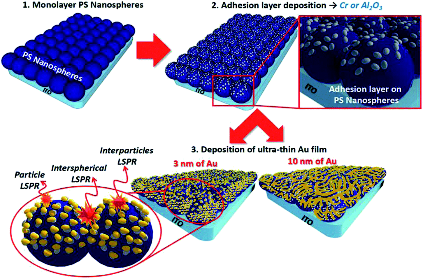 | ||
| Fig. 1 Fabrication flow of AuIoN substrates and LSPR incidence. | ||
3. Results and discussion
A three-dimensional (3D) hybrid hierarchical nanoscale construction allows the intrinsically driven self-assembly of metamaterials.47 The 3D structure is more beneficial than a planar one, especially in SERS, owing to the enormous surface area for target molecule immobilization and a distant track for light propagation in the third dimension.48 In this study, we presented the drop-casting NSL of 100 nm PS nanospheres as the first stage of SERS substrate production. In Fig. 1, it is shown that the HCP and monolayer structures are highly targeted as the initial and fundamental roughening factors to regularly tune the SERS hotspots in the created nanogaps.23,49 Through the proposed structure, LSPRs were synergistically created from the collective electromagnetic fields from the entire AuIoNs structure. The roughness in atomic scale as presented as single adatoms or tiny clustered adatoms prominently leads to the occurrence of a short-range chemical enhancement mechanism. In addition, large-scale roughness (10–100 nm) is highly regarded as a contributor to the enhancement factor through a long-range electromagnetic enhancement mechanism.50In Fig. 2A, as captured by FE-SEM, a large-scale binary lattice of PS nanospheres was successfully formed with about 90% surface coverage. Highly ordered masking particles of small diameter were successfully produced by fixing the PS nanosphere solvent mixture ratio, yielding mutual attractions of both solvents, which created particles–substrate bonding directed towards monolayerity.29 This also resolves the difficulties in centrifugation for particle separation, unlike larger particles which can be easily separated through difference in sedimentation velocity.51 Fig. 2B and C clearly verify the monolayerity and high-order symmetrical structure of the deposited PS nanospheres, with a height of ∼25 nm for each spherical particle, analyzed by AFM. In comparison with the nanosphere diameter, the much smaller height in the AFM measurement was due to the inability of the AFM tip to penetrate and reach the whole curvature because of the tip radius size (∼14 nm) occupation during analysis. The application of spherical masking particles with a small diameter (less than 200 nm) requires meticulous solvent fixation but is beneficial in cutting down the process of particle reduction, which typically incorporates oxygen plasma treatment.29,41 However, when using plasma treatment, undesirable non-close-packed patterns of the masks persist. In this instance, NSL for the deposition of particles as small as 100 nm in diameter in our work reflects an easier and more facile process towards monolayer templating.
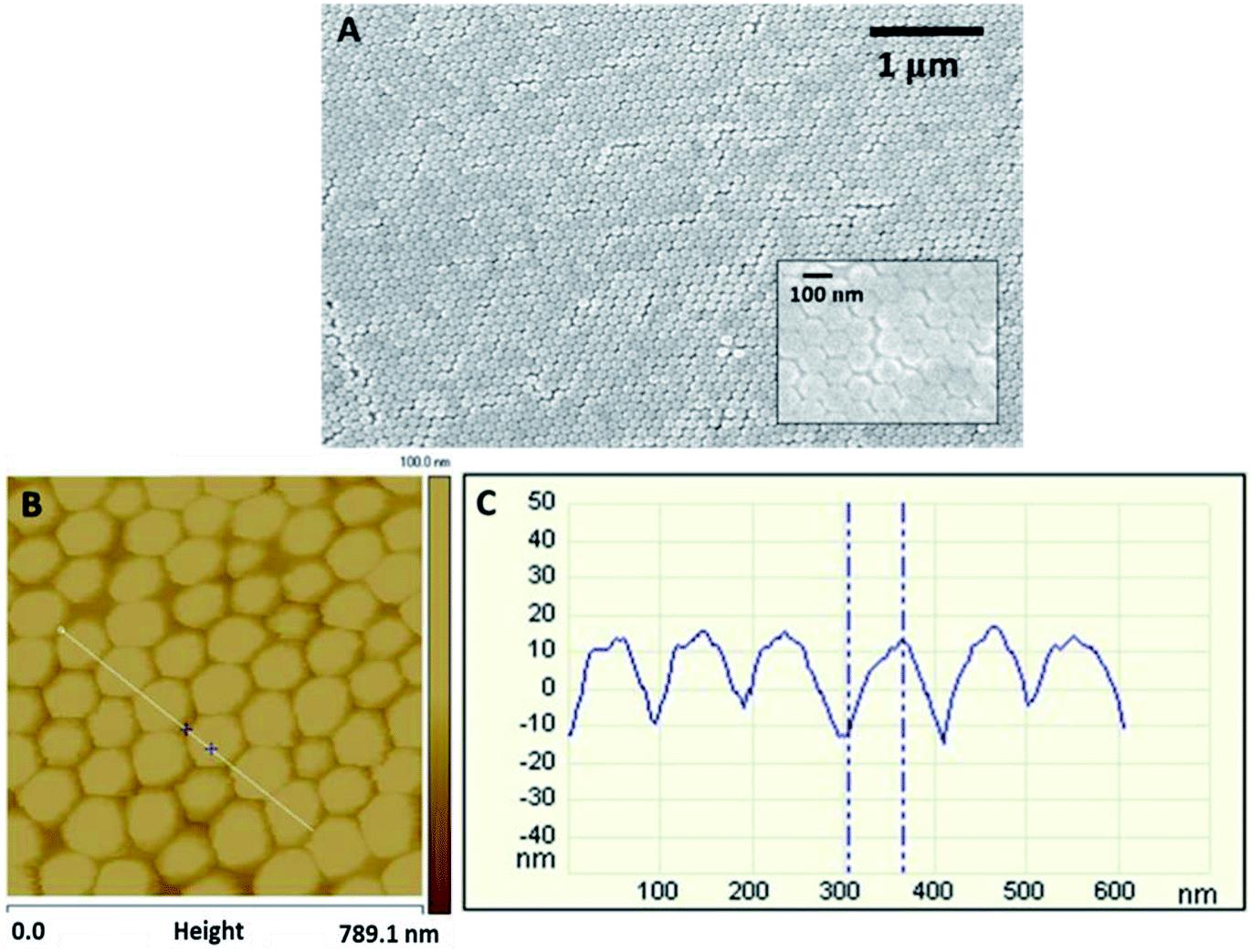 | ||
| Fig. 2 (A) FE-SEM image of monolayer PS nanospheres (d = 100 nm) produced by a drop-casting NSL technique (inset: the magnified image of (A)), (B) AFM images and a set-up for vertical distance measurement, taken between two blue spots, (C) representation of the particle height distribution of the PS nanosphere mask. | ||
Adhesion involves material atomic bonding in forming a film–substrate system depending on the mechanical behavior of the contacting materials. Based on the FE-SEM observation, the application of adhesion layer materials for supporting Au film deposition with various thicknesses strongly impacted the morphology of the substrates. As portrayed in Fig. 3A and B, the AuIoN made up of 3 nm thick Au, deposited on either a Cr or an Al2O3 support layer showed the propensity to form isolated nanoislands, nucleating and coalescing with each other. An apparent protrusive dotted appearance was yielded by the deposition of the thin Au film on the Al2O3 adhesion layer with higher particle density, while spheres decorated with bigger dots were generated on the substrate supported with a Cr adhesion layer. In contrast, as displayed in Fig. 3C and D, the AuIoN from 10 nm thick Au produced apparent island-like nanostructures which appear like elongated islands on the Al2O3 and big globular islands on Cr adhesion layers. The diffusion of Au onto the PS nanosphere covered substrate had been initiated by the first arrival of the vapor phase carrying Au adatoms, and proceeded further during the exchange of interatomic energy between the adatoms and the substrate atoms and between the adatoms themselves.52 A visible protrusion tends to emerge in thinner Au film due to the limited number of continuously arriving atoms from the vapor phase, while in the thicker film, the competitive adatom joining rate is high and, thus, some atoms are buried under the newcomers, resulting in numbers of occurrences, such as refraction and inelastic and elastic reflection.
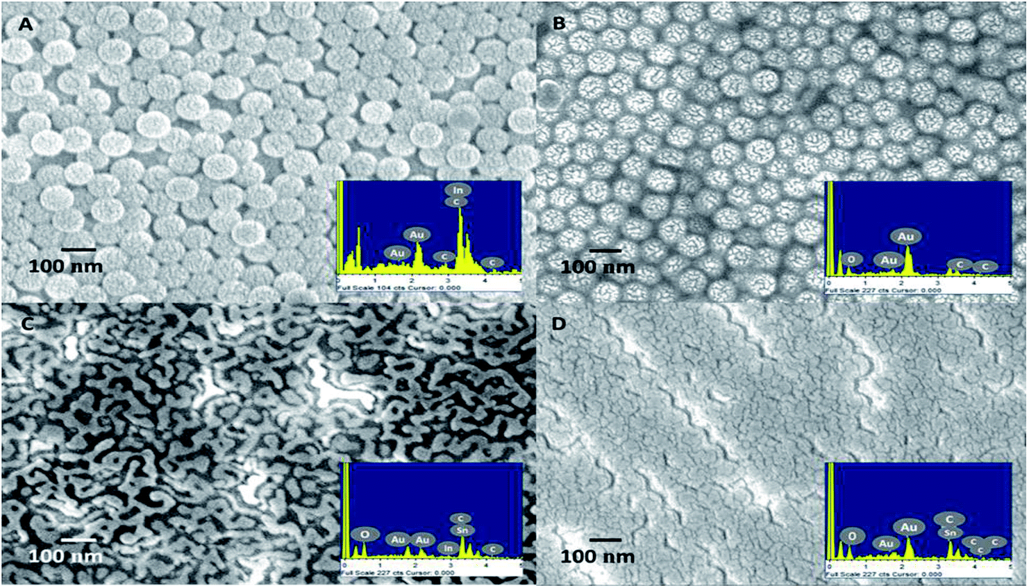 | ||
| Fig. 3 FE-SEM profiles of AuIoN made up of 3 nm thick Au on (A) Al2O3 and (B) Cr adhesion layers, and 10 nm thick Au on (C) Al2O3 and (D) Cr adhesion layers. Insets of each figure show the EDX spectrum validation of the Au element deposited onto the modified substrate. | ||
Moreover, the higher density of Au nanoparticles grown on the PS is a consequence of the lower density of the Al2O3 adhesion layer (3.95 g cm−3) than the basic intrinsic character of Cr (7.19 g cm−3). This property affects the nucleation process when the initial formation layer is formed, in which Cr forms a larger island of a few nanometers thickness compared to Al2O3. In this sense, the Au layer tended to follow the distribution of Cr or Al2O3 as the adhesion layer. Therefore, the gap between the adhesion layer islands will not be as well filled with gold. We strongly believe that this morphological characteristic of the Al2O3 adhesion layer is an advantage for enhancing the plasmonic field between the nanoislands. Not only that, other essential factors in the coalescence of two solid nanoparticles, including physisorption (physical adsorption) and chemisorption generating the retention of metal atoms, must be taken into account. A reduction in the surface energy and a rise in temperature were likely to occur in the coalescence and collision during the growth of metallic nanoparticles53 leading to variation in the structure of the grown particles and the response of the substrate material toward this phenomenon. These findings are in line with the reports of Szunerits et al., 2008, and Schaub et al., 2019, which pinpointed the possibility of vertical and horizontal thickness growth in evaporated Au. A continuous increase in Au thickness contributes to the homogeneity of the layer, while the globular structure is less pronounced as well as the surface roughness.54,55 Additionally, the curvature of PS also contributes to the uniformly bound Au through the thermal evaporation mechanism. Thermal evaporation enables the penetration of the metal even into the hidden crevices within the PS nanoball templates through its unidirectional vaporization. However, the uniformity of the AuIoNs was relatively impacted not only by the natural curvature of the PS nanoballs but also by the regular order of the template. From our findings, despite few dislocations of the PS nanoballs, it was noticed that the uniformity of the spherical template covered a considerably high portion of the surface area. PS nanoball uniformity was the backbone for further metal deposition onto it. A thinner Au film deposited onto the PS nanoballs tends to result in more prominent uniformity pertaining to its dot-like structure than a thicker film in island-like formation. Such combinations could be the key to uniformity enhancement in colloidal-based templating as an alternative to conventional photolithography nanostructuring.
The interparticle gap distances and particle sizes obtained from the average size of the clustered particles were then measured in an FE-SEM system and are summarized in Table 1 to comprehend the LSPR influence correlated to SERS hotspot effectivity. In the group of AuIoNs using super-thin Au film (3 nm), the nanogaps generated were about 5 nm with the support of Al2O3 adhesion layers. This distance is smaller than the AuIoN constructed by 3 nm Au on Cr which roughly created nanogaps of around 17 nm. In addition, the Al2O3 adhesion layer successfully provided higher coverage and density with smaller dots than that supported by the Cr adhesion layer (Fig. 3A and B). In the process of using 10 nm thick Au, the nanogaps created from the adhesion support of Al2O3 were seen to be slightly bigger than those in the Au deposited on Cr, at around 30 nm, plausibly due to the effects of the elongated islands creating larger interstices. The interparticle distance which is critical in plasmonic enhancement refers to the distance within Au particles (either in dots/particles or island structures) and not within PS templates. It is also important to note that in the use of 10 nm thick Au, despite its elongated island morphological appearance, the effect of Au atom clustering during the deposition process was still present. Thus, the islands formed plausibly resulted in island-to-island interspacing with a distance larger than 10 nm. The elongated islands shown by the adhesion support of Al2O3 for 10 nm Au concomitantly resulted in a smaller particle size (Fig. 3C) than those grown on the Cr-assisted substrate (Fig. 3D). In fact, most adhesion layers with a thickness of ∼2 nm form an almost continuous film,56 yet, with respect to Al2O3, the elongated islands were likely generated by a robust metallic bonding reinforced by the presence of the Al-rich interfaces and admixture of covalent bonding from oxygen-rich interfaces.42 The reproducibility of the AuIoNs structure was greatly supported by fundamental masking using PS nanospheres, which in this work has been demonstrated through highly ordered and downscaled PS-based templating for AuNPs, combining a novel and potential Au adhesion layer. High reproducibility can be obtained by the ease of NSL while the AuIoN LSPR activity was easily tuned by the thickness of the deposited Au film. In this fabrication technique, reproducibility is not predominantly assessed by the regularity of the nanostructure shape but more by the orderliness of the interparticle gaps, which are important SERS parameters. This is further confirmed in Fig. 5, which represents considerable prominent reproducibility of the SERS intensity measured in different areas.
| AuIoN interstitial characteristics | Al2O3 + 3 nm Au | Cr + 3 nm Au | Al2O3 + 10 nm Au | Cr + 10 nm Au |
|---|---|---|---|---|
| Particle size (nm) | ∼10 | ∼15 | ∼35 | ∼45 |
| Nanogap (nm) | ∼5 | ∼17 | ∼30 | ∼20 |
In establishing effective SERS hotspots, one key towards the surface enhancement factor of Raman scattering is the nanoscale film roughness. The surface roughness determines several impactful factors, including the metal surface exposed area and the comprehensive interaction of the light with the metal at the nanoscale level. In the AFM observation of the AuIoN using the deposited 3 nm Au, the hexagonally close-packed symmetry could clearly be observed due to the ultra-thin and fine particle sizes of Au on the nanosphere templates. In regard to the surface roughness displayed in Fig. 4A and B, the Al2O3 adhesion layer yielded a substantially higher Rq value than Cr, given by 9.3 nm and 7.4 nm, respectively. This finding indicates that the Al2O3 is likely to be capturing more Au particles when deposited in a very low thickness with a small occurrence of Au clustering, which increases the dot-to-dot arrangement and results in a higher surface roughness when more clustered globular Au are formed. Whereas, with the application of a thicker Au film at 10 nm, the surface topology displays variances either shown in the interfacial image or in the higher Rq value when compared to the growth of particles from 3 nm thick Au film, as a consequence of the thicker film deposition. Few dislocations of the spherical-like curvatures were seen in the group of AuIoNs using 10 nm Au film. The outcome can be deciphered from the evidence that the deposition of metallic film in MFoN construction involves complex interactions entangling strong enforcement of two gratings composed of half-shells and truncated tetrahedra that exist in the spaces between the spheres.23,57
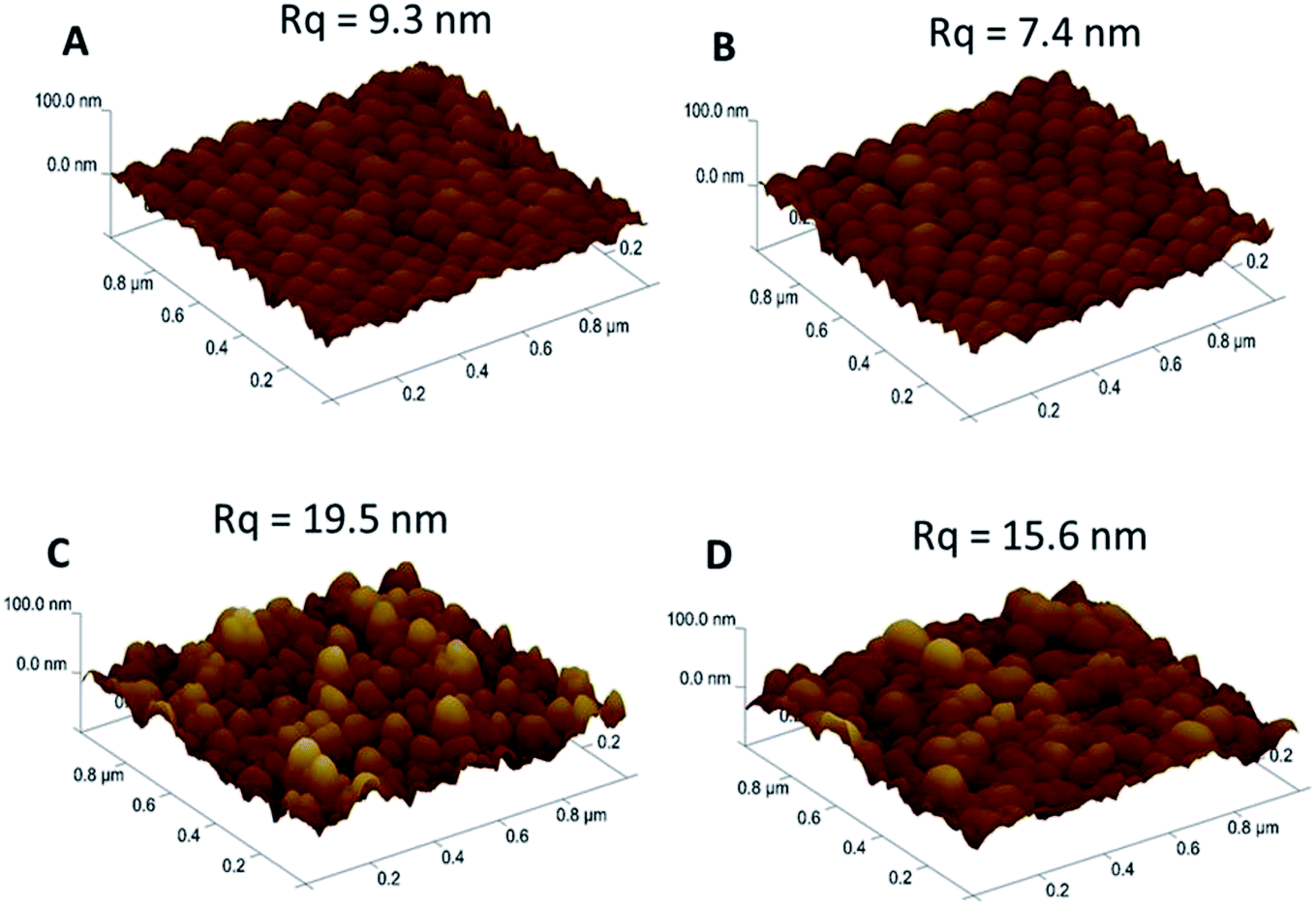 | ||
| Fig. 4 Surface roughness of AuIoN substrates made up of 3 nm thick Au on (A) Al2O3 and (B) Cr adhesion layers, and 10 nm thick Au on (C) Al2O3 and (D) Cr adhesion layers. | ||
 | ||
| Fig. 5 (A) SERS spectra of the AuIoN compared to Au deposition on ITO without a PS template, (B) the zoomed image of Au deposition on ITO without a PS template, (C) normal Raman spectrum of 1 μM R6G. | ||
Subsequently, it is noticeable that the Al2O3 employed as an adhesion layer for both 3 and 10 nm Au film, had yielded higher surface roughness in comparison with the Cr adhesion layer. Cr is renowned as a material with a high inter-diffusion rate, which consequently alleviates the adhesion forces of the metallic film when in contact with high temperature. In addition, the high inter-diffusion rate, which does not easily reach a stable state, remains problematic in the application of a Cr adhesion layer. On the other hand, the higher number of Au particles and film density on the Al2O3 supporting layer can be elucidated by the nature of the process in alumina evaporation generating a non-stoichiometric film due to oxygen deficiency.58 Under a high-temperature ambiance, oxygen gas flow reinforces oxidation, improving the stability of the oxide film through a decrease in stoichiometric imbalance.43
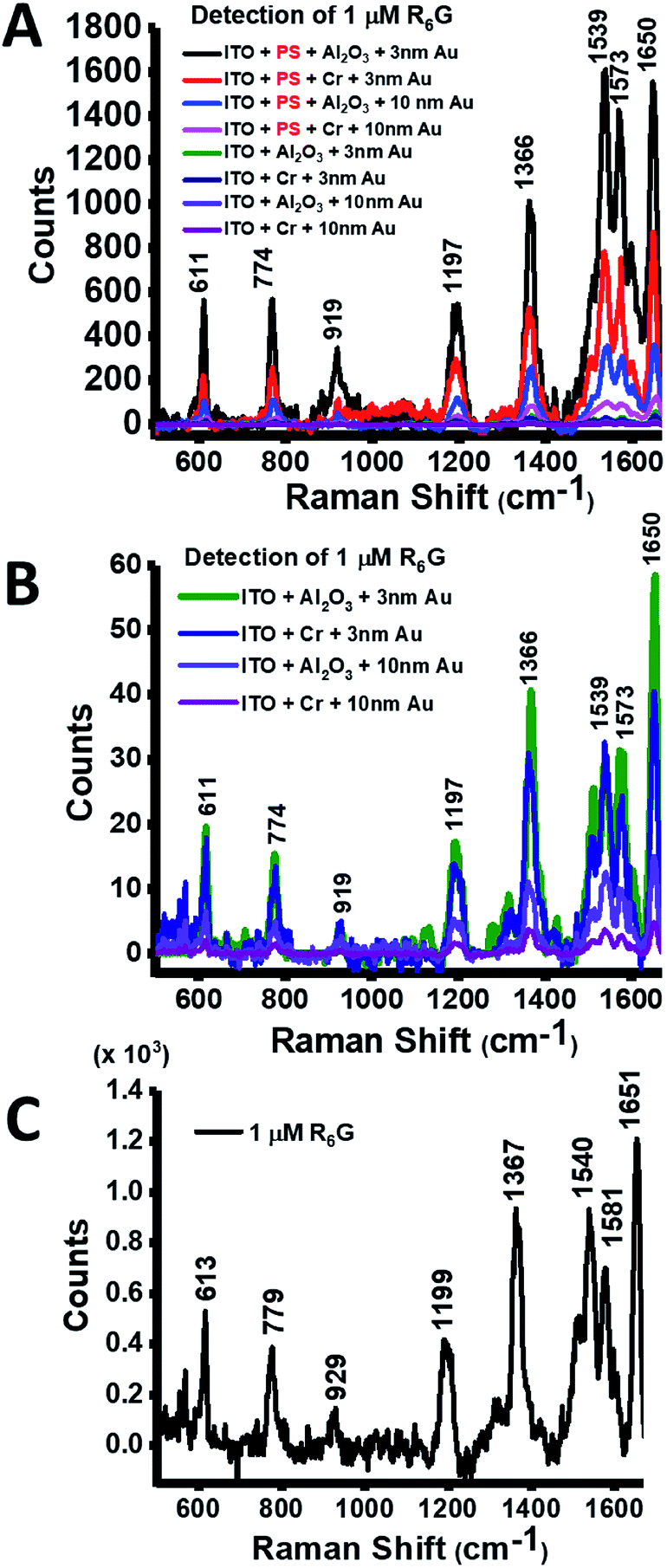
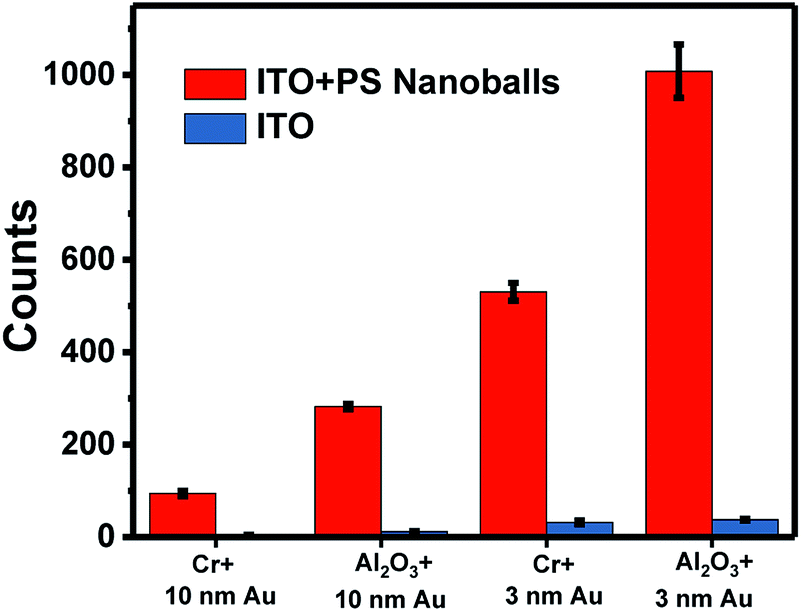
To gain a profound understanding on the impact of the natural roughening through the assembled spherical curvature of PS nanospheres, SERS measurement was conducted on both PS nanosphere uncovered and covered ITO substrates for Au deposition. Fig. 5 demonstrates the average SERS intensity of each modification condition taken from ten different points of measurement. As can be seen in Fig. 5A, in all AuFoN substrates regardless of Au thickness or adhesive layers used, the PS nanosphere masking had created more intense hotspots, as demonstrated by more optimum SERS peaks for R6G molecule detection than for the substrate with an Au film deposited on bare ITO. In a complex observation of the AuIoN groups, as seen in Fig. 5A and B, the highest SERS spectrum was gained by 3 nm Au on Al2O3, followed by 3 nm Au on Cr, 10 nm Au on Al2O3 and 10 nm Au on Cr adhesion layers, respectively. The characteristic Raman peaks of the R6G molecules became more pronounced and the main groups of modes corresponding to C–C–C ring in-plane bending at around 611 cm−1, out-of-plane bending at around 779 cm−1 and ring breathing (RB), such as aromatic C–C stretching at around 1199 and 1367 cm−1, were clearly recorded. Additionally, some intense Raman bands at around 929, 1540, 1581 and 1651 cm−1 were observed and found to be consistent with formerly published reports,29,59,60 as also shown in the normal R6G Raman spectrum in Fig. 5C. Accordingly, the enhancement in the local field in the AuIoN groups as an outcome of noble metal aggregation also showed a tendency to redshift the SPR in Raman analysis61 presented by the lower Raman shift number of AuIoNs made up with Al2O3 in both Au thicknesses as compared to the AuIoNs applying a Cr adhesion layer, as seen in the peak area of around 611 cm−1 for AuIoN using Al2O3 for 10 nm thick Au, while that of using Cr adhesion for the same Au thickness deposition resulted in a peak at 620 cm−1. Similar trends were shown for the peaks around 777 cm−1 and 929 cm−1.
Furthermore, the paramount characteristics of the thinner Au film are closely linked with the synergistic impacts of the optimum particle density and smaller particle size creating effective interstitial plasmonic hotspots and contributing scattering effects by an enhancement in the extinction intensity as well as the tunability for the plasmon resonance wavelength.62 In contrast, in the thicker film, the nucleated void density is lessened but results in wider void opening during dewetting to reach a stable configuration and, therefore, leads to an increment in the gap spacing between Au islands.63,64 Nevertheless, in all the treatment groups, in either substrates without PS nanospheres or substrates with PS nanospheres, the Al2O3 adhesion layer successfully performed more effective SERS in comparison with Cr (Fig. 5A and B). A higher density of Au was shown on the Al2O3 support layer than on the Cr, which concomitantly confirms the larger interatomic bonding of the Al2O3 than the Cr layer, as reported by Guarnieri, et al., in 2014.43 Additionally, these outcomes also attest that higher metallic bonding between the Au film on Al2O3 than on Cr was due to the presence of the wider range of interfacial adhesion and stoichiometry provided by the Al2O3 compound than in Cr as a single element. This can be explained by the interfacial stoichiometry of Al2O3, which can be stoichiometric, oxygen-rich, or aluminum-rich in a qualitative way, consisting of the stoichiometry of the Al2O3 metal/alumina interface ((M/Al2O3)A11), the aluminum-rich part joining metal ((M/Al2O3)A12) and oxygen-rich part ((M/Al2O3)O), with a notable electron density parameter at the boundary for Au at 3.87 d.u. (density unit).37
The illustrations in Fig. 6A and B can describe the underlying mechanism of LSPR enhancement for SERS on an AuIoN substrate. First, the R6G should be immobilized in the gold nanoisland areas, so the larger the surface area of the gold nanoislands, the higher the possibility of immobilization of R6G particles on the AuIoN substrate. Moreover, the critical role of electron transitions from the gold nanoislands to the R6G HOMO level energy is greatly contributed by the LSPR field. The stronger the LSPR field, the higher the energy level of the LSPR, improving the electron transition to the upper level energy. Therefore, the electron injection to the HOMO level will be enormous when the LSPR field is actively generated in the gold nanoislands. Consequently, it will result in SERS signal enhancement due to the larger amount of electron transitions from the HOMO to the LUMO level in the R6G molecules.
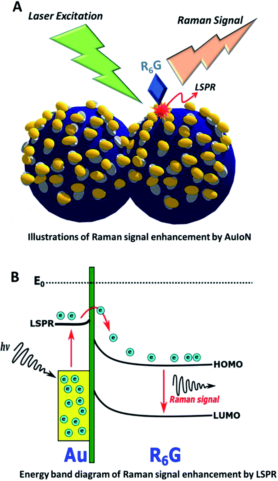 | ||
| Fig. 6 (A) The mechanism of Raman signal enhancement on AuIoN structures and (B) the band diagram showing the transition of the electron in the R6G probe. Electron transitions occur from the gold nanoislands to the R6G HOMO towards the LUMO level due to LSPR. | ||
The SERS enhancement factor (EFSERS) is calculated based on the equation below:29,65
 | ||
| Fig. 7 The reproducibility of the intensity of R6G peak at ∼1366 cm−1 on AuIoN structures extracted from 10 points of measurement. | ||
The highly geometrical active sites were simulated using finite difference time domain (FDTD) methods by tracing the electromagnetic (EM) field enhancement of the AuIoN trimers on interconnected AuIoN with both dispersive layers. In Fig. 8, the AuIoN employing Al2O3 as an adhesion layer for 3 nm Au demonstrated the highest range of electromagnetic (EM) field enhancement, while the lowest range was shown by AuIoN using Cr for 10 nm Au film. In all the AuIoNs, it is demonstrated that the distribution of the near-field intensity is greatly augmented in the boundary between the adjacent Au spheres. The simulation corresponds linearly to our SERS findings where the EM field was higher with the deposition of 3 nm thick Au than with 10 nm. In addition, the stronger EM fields can be clearly captured between the crevices formed by two adjacent Au spheres regarded as SERS hotspot locations. The sharp crevices between the neighbouring AuIoNs have been remarkably acknowledged for their ability to provide favorable geometrical circumstances for electromagnetic field localization and very large SERS enhancements.23 The simulation confirms the contribution of interparticle Au LSPR covering the nanospheres and the interspherical LSPR giving out the most intense EM field reinforcement within AuIoN crevices.
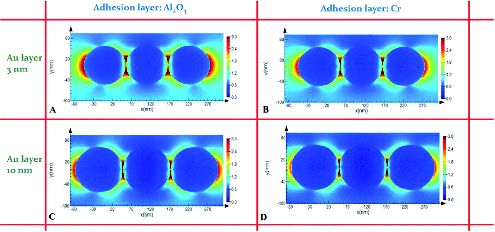 | ||
| Fig. 8 2D FDTD simulation of electric field distribution on AuIoN substrates made up of 3 nm Au on (A) Al2O3 and (B) Cr adhesion layers, and 10 nm Au on (C) Al2O3 and (D) Cr adhesion layers. | ||
4. Conclusions
The impact of adhesion layers and the thinness of Au film on AuIoN structures synergistically enhanced SERS activity through the synergistic collective near-field intensity. The application of Al2O3 as an adhesion layer for ultra-thin Au demonstrated higher metallic bonding than the typical Cr adhesion layer, which simultaneously resulted in higher particle density on the surface affecting LSPR activity for SERS activity enhancement. Moreover, the LSPR improvement contributed by AuIoN “step-by-step modification” was shown through the improvement in surface roughness and interstitial nanojunctions creating highly effective SERS hotspots. Not only that, the regions of the Al2O3 adhesion layer for Au, including their stoichiometry, and aluminum-rich and oxygen-rich interfaces, were noted to be substantial to resolve the problems of high inter-diffusion in Cr application for the Au adhesion layer, and can potentially be applied for various purposes in plasmonic device fabrication, such as in SERS-based biological and chemical detection.Conflicts of interest
There are no conflicts to declare.Acknowledgements
C. S. L., C. M. Y. and Y. C. T. express a heartfelt gratitude to Chang Gung Memorial Hospital (CGMH) Taiwan, for the financial support under contract no. of CMRPD2G0102; Ministry of Science and Technology (MOST) Taiwan under the contract number of MOST 107-2911-I-182-502 and MOST 107-2218-E-182-006. A. P. thanks the Kurita Water and Environment Foundation (KWEF) Japan and Asian Institute of Technology (AIT) Thailand for Kurita-AIT Research Grant 2018; and the Indonesian Institute of Sciences.References
- S. S. Singha, S. Mondal, T. S. Bhattacharya, L. Das, K. Sen, B. Satpati, K. Das and A. Singha, Biosens. Bioelectron., 2018, 119, 10–17 CrossRef CAS PubMed.
- B. Fazio, C. D'Andrea, A. Foti, E. Messina, A. Irrera, M. G. Donato, V. Villari, N. Micali, O. M. Maragò and P. G. Gucciardi, Sci. Rep., 2016, 6, 26952 CrossRef CAS PubMed.
- N. Feliu, M. Hassan, E. Garcia Rico, D. Cui, W. Parak and R. Alvarez-Puebla, Langmuir, 2017, 38, 9711–9730 CrossRef PubMed.
- B. A. Prabowo, Y.-F. F. Chang, H.-C. C. Lai, A. Alom, P. Pal, Y.-Y. Y. Lee, N.-F. F. Chiu, K. Hatanaka, L.-C. C. Su and K.-C. C. Liu, Sens. Actuators, B, 2018, 254, 742–748 CrossRef CAS.
- S.-Y. Ding, J. Yi, J.-F. Li, B. Ren, D.-Y. Wu, R. Panneerselvam and Z.-Q. Tian, Nat. Rev. Mater., 2016, 1, 16021 CrossRef CAS.
- Q. Zhang, X. Li, Q. Ma, Q. Zhang, H. Bai, W. Yi, J. Liu, J. Han and G. Xi, Nat. Commun., 2017, 8, 14903 CrossRef PubMed.
- B. A. Prabowo, R. Y. L. Wang, M. K. Secario, P.-T. Ou, A. Alom, J.-J. Liu and K.-C. Liu, Biosens. Bioelectron., 2017, 92, 186–191 CrossRef CAS PubMed.
- E. Lengert, A. M. A. M. Yashchenok, V. Atkin, A. Lapanje, D. A. D. A. Gorin, G. B. G. B. Sukhorukov and B. V. B. V. Parakhonskiy, RSC Adv., 2016, 6, 20447–20452 RSC.
- L. Huang, J. Wan, X. Wei, Y. Liu, J. Huang, X. Sun, R. Zhang, D. D. Gurav, V. Vedarethinam, Y. Li, R. Chen and K. Qian, Nat. Commun., 2017, 8, 220 CrossRef PubMed.
- H. Wei, S. M. Hossein Abtahi and P. J. Vikesland, Environ. Sci.: Nano, 2015, 2, 120–135 RSC.
- R. Verma and B. D. Gupta, Food Chem., 2015, 166, 568–575 CrossRef CAS PubMed.
- R. M. Davis, J. L. Campbell, S. Burkitt, Z. Qiu, S. Kang, M. Mehraein, D. Miyasato, H. Salinas, J. Liu and C. Zavaleta, Nanomaterials, 2018, 8, 953 CrossRef PubMed.
- J. Wu, P. Wang and Y. Fang, Nanomaterials, 2018, 8, 864 CrossRef PubMed.
- J. Quan, J. Zhang, X. Qi, J. Li, N. Wang and Y. Zhu, Sci. Rep., 2017, 7, 14771 CrossRef PubMed.
- D. Radziuk and H. Moehwald, Phys. Chem. Chem. Phys., 2015, 17, 21072–21093 RSC.
- Q. Tao, S. Li, C. Ma, K. Liu and Q.-Y. Zhang, Dalton Trans., 2015, 44, 3447–3453 RSC.
- S. Y. Ding, E. M. You, Z. Q. Tian and M. Moskovits, Chem. Soc. Rev., 2017, 46, 4042–4076 RSC.
- B. A. Prabowo, A. Purwidyantri and K.-C. Liu, Biosensors, 2018, 8, 80 CrossRef PubMed.
- H. Wei, K. Rodriguez, S. Renneckar, W. Leng and P. J. Vikesland, Analyst, 2015, 140, 5640–5649 RSC.
- Q. Zhang, N. Large, P. Nordlander and H. Wang, J. Phys. Chem. Lett., 2014, 5, 370–374 CrossRef CAS PubMed.
- V. V. Thacker, L. O. Herrmann, D. O. Sigle, T. Zhang, T. Liedl, J. J. Baumberg and U. F. Keyser, Nat. Commun., 2014, 5, 3448 CrossRef PubMed.
- J. F. Wang, X. Z. Wu, R. Xiao, P. T. Dong and C. G. Wang, PLoS One, 2014, 9, e9797 Search PubMed.
- C. Farcau and S. Astilean, J. Phys. Chem. C, 2010, 114, 11717–11722 CrossRef CAS.
- A. Purwidyantri, L. Kamajaya, C.-H. Chen, J.-D. Luo, C.-C. Chiou, Y.-C. Tian, C.-Y. Lin, C.-M. Yang and C.-S. Lai, J. Electrochem. Soc., 2018, 165, H3170–H3177 CrossRef CAS.
- F. Lu, K. G. Yager, Y. Zhang, H. Xin and O. Gang, Nat. Commun., 2015, 6, 6912 CrossRef CAS PubMed.
- P. C. Wuytens, A. G. Skirtach and R. Baets, Opt. Express, 2017, 25, 12926–12934 CrossRef CAS PubMed.
- T. J. Wang, K. C. Hsu, Y. C. Liu, C. H. Lai and H. P. Chiang, J. Opt., 2016, 18, 055006 CrossRef.
- A. Purwidyantri, C.-H. Chen, B.-J. Hwang, J.-D. Luo, C.-C. Chiou, Y.-C. Tian, C.-Y. Lin, C.-H. Cheng and C.-S. Lai, Biosens. Bioelectron., 2016, 77, 1086–1094 CrossRef CAS PubMed.
- A. Purwidyantri, I. El-Mekki and C.-S. Lai, IEEE Trans. Nanotechnol., 2017, 16, 551–559 CAS.
- J. Chen, J.-F. Wang, X.-Z. Wu, Z. Rong, P.-T. Dong and R. Xiao, J. Nanosci. Nanotechnol., 2018, 18, 3825–3831 CrossRef CAS PubMed.
- H. T. Ngo, H. N. Wang, A. M. Fales and T. Vo-Dinh, Anal. Chem., 2013, 85, 6378–6383 CrossRef CAS PubMed.
- Y. Yang, T. Qiu, F. Kong, J. Fan, H. Ou, Q. Xu and P. K. Chu, J. Appl. Phys., 2012, 111, 21–24 Search PubMed.
- M. Kang, M. Losego, E. Sachet, J. P. Maria and S. Franzen, ACS Photonics, 2016, 3, 1993–1999 CrossRef CAS.
- C. Rhodes, M. Cerruti, A. Efremenko, M. Losego, D. E. Aspnes, J. Maria, S. Franzen, C. Rhodes, M. Cerruti, A. Efremenko, M. Losego, D. E. Aspnes and J. Maria, J. Appl. Phys., 2008, 103, 093108 CrossRef.
- W. Wei, R. Hong, M. Jing, W. Shao, C. Tao and D. Zhang, Nanotechnology, 2017, 29, 1 Search PubMed.
- J. Yang, F. Ren, X. Chong, D. Fan, S. Chakravarty, Z. Wang, R. Chen and A. Wang, Photonics, 2014, 1, 380–389 CrossRef PubMed.
- F. Colas, D. Barchiesi, S. Kessentini, T. Toury and M. L. D. La Chapelle, J. Opt., 2015, 17, 114010 CrossRef.
- T. Siegfried, Y. Ekinci, O. J. F. Martin and H. Sigg, ACS Nano, 2013, 7, 2751–2757 CrossRef CAS PubMed.
- S. J. Madsen, M. Esfandyarpour, M. L. Brongersma and R. Sinclair, ACS Photonics, 2017, 4, 268–274 CrossRef CAS PubMed.
- M. Todeschini, A. Bastos Da Silva Fanta, F. Jensen, J. B. Wagner and A. Han, ACS Appl. Mater. Interfaces, 2017, 9, 37374–37385 CrossRef CAS PubMed.
- Z. Zhu, Q. Li, B. Bai and S. Fan, Nanoscale Res. Lett., 2014, 9, 25 CrossRef PubMed.
- H. T. Li, L. F. Chen, X. Yuan, W. Q. Zhang, J. R. Smith and A. G. Evans, J. Am. Ceram. Soc., 2011, 94, S154–S159 CrossRef CAS.
- V. Guarnieri, L. Biazi, R. Marchiori and A. Lago, Biomatter, 2014, 4, e28822 CrossRef PubMed.
- N. Sultanova, S. Kasarova and I. Nikolov, Acta Phys. Pol., A, 2009, 116, 585 CrossRef CAS.
- M. J. Weber, Handbook of Optical Materials, CRC Press, 2002 Search PubMed.
- P. B. Johnson and R. W. Christy, Phys. Rev. B: Solid State, 1972, 6, 4370 CrossRef CAS.
- I. Levchenko, K. Bazaka, M. Keidar, S. Xu and J. Fang, Adv. Mater., 2018, 30, 1702226 CrossRef PubMed.
- X. Zhang, X. Xiao, Z. Dai, W. Wu, X. Zhang, L. Fu and C. Jiang, Nanoscale, 2017, 9, 3114–3120 RSC.
- L. A. Wu, W. E. Li, D. Z. Lin and Y. F. Chen, Sci. Rep., 2017, 7, 13066 CrossRef PubMed.
- L. A. Dick, A. D. McFarland, C. L. Haynes and R. P. Van Duyne, J. Phys. Chem. B, 2002, 106, 853–860 CrossRef CAS.
- P. Qiu and C. Mao, Adv. Mater., 2011, 23, 4880–4885 CrossRef CAS PubMed.
- F. Ruffino and M. Grimaldi, Coatings, 2018, 8, 121 CrossRef.
- J. Antunez-Garcia, S. Mejia-Rosales, E. Perez-Tijerina, J. M. M. Carrizales and M. Jose-Yacaman, Materials, 2011, 4, 368–379 CrossRef CAS PubMed.
- S. Szunerits, V. G. Praig, M. Manesse and R. Boukherroub, Nanotechnology, 2008, 19, 195712 CrossRef PubMed.
- A. Schaub, P. Slepička, I. Kašpárková, P. Malinský, A. Macková and V. Svorčík, Nanoscale Res. Lett., 2013, 8, 249 CrossRef PubMed.
- W. Liu, K. Chikkadi, M. Muoth, C. Hierold and M. Haluska, Nanotechnology, 2015, 27, 015201 CrossRef PubMed.
- L. Baia, M. Baia, J. Popp and S. Astilean, J. Phys. Chem. B, 2006, 110, 23982–23986 CrossRef CAS PubMed.
- F. Lewis, S. Turgeon, P. Chevallier, J. J. Pireaux, M. Tatoulian and D. Mantovani, Plasma Processes Polym., 2010, 7, 309–317 CrossRef CAS.
- K. Zhang, T. Zeng, X. Tan, W. Wu, Y. Tang and H. Zhang, Appl. Surf. Sci., 2015, 347, 569–573 CrossRef CAS.
- P. Hildebrandt and M. Stockburger, J. Phys. Chem., 1984, 88, 5935–5944 CrossRef CAS.
- F. Tian, F. Bonnier, A. Casey, A. Shanahan and H. Byrne, Anal. Methods, 2014, 6, 9116–9123 RSC.
- M. Kang, S.-G. Park and K.-H. Jeong, Sci. Rep., 2015, 5, 14790 CrossRef CAS PubMed.
- E. Jiran and C. V. Thompson, J. Electron. Mater., 1990, 19, 1153–1160 CrossRef CAS.
- D. Wang, R. Ji and P. Schaaf, Beilstein J. Nanotechnol., 2011, 2, 318–326 CrossRef CAS PubMed.
- A. B. Serrano-montes, D. J. De Aberasturi, J. Langer, J. J. Giner-casares, L. Scarabelli, A. Herrero and L. M. Liz-marza, Langmuir, 2015, 31, 9205–9213 CrossRef CAS PubMed.
- Y. Liu, S. Xu, H. Li, X. Jian and W. Xu, Chem. Commun., 2011, 47, 3784–3786 RSC.
- W.-L. Zhai, D.-W. Li, L.-L. Qu, J. S. Fossey and Y.-T. Long, Nanoscale, 2012, 4, 137–142 RSC.
| This journal is © The Royal Society of Chemistry 2019 |