
 Open Access Article
 This Open Access Article is licensed under a Creative Commons Attribution-Non Commercial 3.0 Unported Licence
Optimization of a hybrid plasmonic configuration: particle on a corrugated film and its SERS application†
Ming Zhuo,
Chaoguang Wang *,
Peitao Dong,
Jian Chen and
Xuezhong Wu*
*,
Peitao Dong,
Jian Chen and
Xuezhong Wu*
College of Mechatronics Engineering and Automation, National University of Defense Technology, Changsha, Hunan 410073, P. R. China. E-mail: xuezhongwu@nudt.edu.cn
First published on 30th October 2019
Abstract
Hybrid SERS configurations, which combine manufactured metallic chips with nanoparticles, have emerged as powerful and promising SERS substrates because they not only provide cost-effective and high-yield manufacture, but also demonstrate excellent sensitivity and outstanding reproducibility. Herein, a plasmonic hybrid structure, a particle on an Au film over nanoparticles (particle-AuFON) configuration, was studied for SERS application. In a previous study, we constructed a hybrid substrate by grafting Au@Ag core–shell NPs onto the AuFON structure. In this study, the hybrid substrate is designed and simulated to optimize electromagnetic enhancement while also affording exceptional uniformity, repeatability and stability, which are essential factors in SERS applications. This hybrid substrate provides good SERS performance with a detection limit of 1 × 10⁻¹⁰ M, which is 100-fold improvement compared to AuFON substrate or Au@Ag NPs. The excellent signal enhancement originates from the hotspot improvement and densification, as visualized by the FDTD calculations. Additional hotspots were created at the gaps between the Au@Ag NPs and the AuFON, thus improving the density of hotspots. Moreover, the intensity of the hotspots was improved due to EM coupling between the original hotspots and additional hotspots. To validate the feasibility of this hybrid substrate in SERS-based detection, melamine was detected as an example. The detection limit was 10 nM, which was much lower than the maximum limit of melamine in infant formula (1 ppm) legislated by the governments of both the United States and China. A calibration curve was plotted between the SERS intensity and melamine concentration with a correlation coefficient of 0.98. This hybrid SERS substrate shows great potential in SERS-based sensing and imaging, as it provides high sensitivity and outstanding reproducibility with a simple fabrication procedure, facilitating the cost-effective and high-yield manufacture of SERS substrates.
1. Introduction
Surface-enhanced Raman scattering (SERS) is a powerful and promising technique, finding potential applications in the fields of physics, in vivo diagnosis, ultra-sensitive bio-chemical sensors, super-resolution optical imaging, etc., because it can provide intrinsic spectrum of the analyte with great signal enhancement reaching up to 106 to 1010. Though not absolutely and widely validated, it is believed that the dramatic observed enhancement originates from both chemical and especially physical electromagnetic (EM) field enhancement. An area where the EM field concentrates or couples is called a hotspot, which plays a fundamental role in SERS measurements. Literature indicates that probes located in a hotspot area contribute 85% of signal intensity in the measurement while they only cover about 6% of the surface area. Thus, considerable endeavours have been made to prepare nanostructures with nanogaps and nanotips, to enrich the EM or chemical enhancement contributions.The reported SERS substrates can be roughly divided into three categories in terms of their morphology and preparation methods. The first type is noble metallic nanostructures manufactured directly on a solid support.1 A variety of methods have been used to prepare metallic nanostructures, such as focused ion beam (FIB) lithography,2 nanoprint lithography (NIL),3 nanosphere lithography,4–18 glancing angle oblique vapor deposition,19–24 annealing25–28 and atomic layer deposition (ALD) separation.
The second type is metallic nanoparticle sol prepared by reducing noble metal ions in solution,29 including Au/Ag NPs,30,31 core–shell NPs,32–34 magnetic core–shell NPs,35,36 self-gapped NPs,37 and DNA-connected dumbbell NPs.38,39 The hotspots were usually created at the nanogaps by means of aggregation. The nanoparticle sol has the advantages of high enhancement factor, controllable morphology, and good bio-compatibility. However, the nanoparticle sol may fail after long-term storage or vibration. Also, the NPs aggregation formation is hard to control precisely, resulting in instability of SERS hot spots.
The third type is a hybrid SERS substrate usually constructed by combining nanostructure with NPs sol. Li's group developed a shell-isolated nanoparticle-enhanced Raman spectroscopy technique.32,40–44 They found that additional hotspots were created or transferred in shell-isolated nanoparticle aggregates when located over noble metal film, facilitating Raman signal improvement. Similar work was done by Yu's group,45,46 Wang's group31 and Shin's group.47,48 In these works, NPs aggregates were assembled on a flat noble metal film. The EM field concentrated, coupled and transferred on the surface of the aggregation, forming a great many hotspots. However, the flat noble metal film itself does not have the ability for signal enhancement. Better SERS performance can be expected if corrugated film is employed, as it has SERS signal enhancement ability itself.
Our group has reported a corrugated film and its hybrid structure combined with Ag NP: it showed better SERS performance than flat film.49 The hybrid structure also showed potential in detecting paraquat.50 But the uniformity, repeatability and long-time stability were not ideal. In this paper, to build a sensitive and stable SERS substrate, binding methods were studied, including physical, small molecule and polymer connections. The structural parameters of the SERS substrate were optimized. The experimental results showed that its sensitivity, uniformity, repeatability and stability were improved. The enhancement mechanism of the substrate was studied by FDTD calculations. Its potential application in SERS-based sensors is validated by its sensitive and selective detection of melamine.
2. Methods
2.1 Materials
R6G, p-aminothiophenol (p-APT) and polyethyleneimine (PEI, branched) were obtained from Sigma-Aldrich (Germany). Silver nitrate (AgNO3), chloroauric acid (HAuCl4), citric acid melamine, trisodium salt dihydrate (C6H5Na3O7·2H2O), ethanol (C2H5OH), etc., were purchased from Sinopharm (Shanghai, China), unless specified otherwise. All chemicals were of analytical reagent grade and used as received. Chromium (Cr) pellets (99.99%) and gold (Au) wire (99.999%) were purchased from Jinyu Aochen (Beijing, China). Silicon (100) wafers were purchased from CETC46 (Tianjin, China). Ultrapure water was obtained from a Millipore Milli-Q system with the resistance rate ≥18.2 MΩ cm.2.2 Preparation of AuFON substrate
The AuFON structure was fabricated by the nanosphere lithography (NSL) technique and employed as the corrugated film.51–53 A sketch of the fabrication is shown in Fig. 1. In brief, polystyrene (PS) beads were self-assembled by spin-coating on the Si wafer to construct a hexagonal close-packed monolayer. To adjust the morphology of the corrugated film, the PS beads were etched by oxygen plasma for various periods, including 2 min, 3 min, 4 min and 5 min. Finally, a gold layer was deposited on the etched PS beads to construct the Au film over nanoparticle structure, as shown in Fig. 2(a). The SEM images of the prepared AuFON substrate are shown in Fig. 2.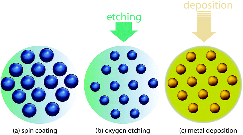 | ||
| Fig. 1 A schematic of the NSL method to prepare AuFON. | ||
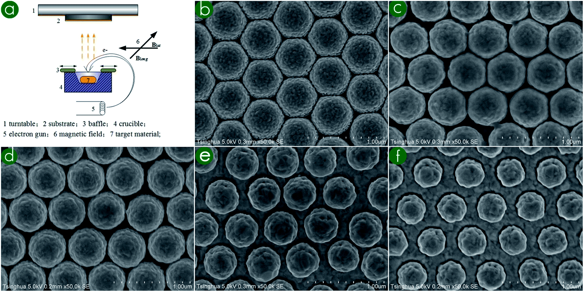 | ||
| Fig. 2 (a) The diagrammatic sketch of the deposition chamber and (b)–(f) SEM images of Au film on PS beads etched for different times. | ||
2.3 Synthesis of Au@Ag core–shell NPs
Au@Ag core–shell NPs were prepared by capping a Ag layer on Au seeds with a reducing agent34 and were employed as the adhered particles. Au NPs with a diameter of 25 nm were synthesized by the citrate reduction method and utilized as seeds. To prepare Au@Ag NPs with various sizes in one pot, a successive addition and successive sampling method was designed and conducted. The diameter of the beads was controlled by adjusting the thickness of the Ag shell. First, Au seed (150 ml) was double diluted and heated to boiling. Excessive sodium citrate solution was added and used as reducing agent. 1500 μl AgNO3 solution (10 mM) was added into the boiling suspension and heated to boiling. After the color of the sol stabilized (about 20 min), 20 ml synthesized sol was removed as a sample. Other addition and sampling processes were conducted in the same way. The details are shown in Table S1 in the ESI.† The concentration of added AgNO3 solution was kept at 0.05 mM. All samples were centrifuged at 7000 rpm for 6 min and dispersed in 20 ml water for use.2.4 Preparation of hybrid SERS substrate
The particle-AuFON configuration was constructed in three ways, including physical connection, small molecule connection and polymer connection. For physical connection, the Au@Ag NPs were dropped onto the AuFON supporting base and utilized directly after drying. For a small molecule connection, the AuFON chip (10 mm × 10 mm) was immersed in the p-ATP solution and vibrated gently for 3 hours, then rinsed vigorously with deionized water. Subsequently, the p-ATP modified chip was immersed in Au@Ag NPs sol for 3 hours with slight shaking, then washed vigorously with deionized water to remove unlinked particles. Finally, the particle-AuFON structure was flushed with nitrogen to dry for use. For a polymer connection, the immobilization process was similar to that of small molecules but employed polyethyleneimine (PEI, branched type) as the binder instead of p-ATP.2.5 FDTD calculation
Commercially obtained software (Lumerical Solutions, Canada) was utilized to visualize the EM field distribution and hotspot generation on the surface of the particle-AuFON configuration. Calculation models were built according to the geometry of the fabricated structure, including single point, two points, and cluster contacts. The dielectric constants of Au, Ag, etc. were those reported by Palik.54 Plane wave with a wavelength of 785 nm was incident in −Z direction with X polarization. Perfectly matched layer absorbing boundary conditions were adopted in all directions. Yee cell is set to 1 nm × 1 nm × 1 nm, which is sufficient to characterize the EM field behavior at the junctions.2.6 Characterization
The morphologies of the AuFON and particle-AuFON structures were characterized with field emission scanning electron microscopy (FE-SEM; Hitachi S-4800, Japan). The morphology of the Au@Ag core–shell NPs was investigated by transmission electron microscopy (TEM, Hitachi H-7650, Japan). The transmission spectra of the Au@Ag core–shell NPs sol were recorded by UV-spectrometer (UV-2600, Shimadzu, Japan). The SERS spectra were collected utilizing a portable Raman system (i-Raman Plus BWS465-785H, B&W Tek., USA). The Raman system was equipped with a diode laser source with excitation wavelength of 785 nm.3. Results and discussion
3.1 Preparation of particle-AuFON configuration
Hybrid plasmonic configuration has great potential for SERS applications because it creates many new hotspots which couple with the original ones, while using low-cost and robust procedures. Herein, the particle on corrugated film structure was constructed by grafting the Au@Ag core–shell nanoparticles onto an AuFON structure, forming a particle-AuFON configuration. To construct the corrugated film in a controlled and periodical way, colloid beads were self-assembled on the supporting base, followed by 100 nm Au deposition. Before the deposition, the PS nanospheres can be etched with oxygen plasma to deepen the gap or separate the PS particles. The process is shown in Fig. 1(a)–(c). The etching chamber is shown in Fig. 1(d).The morphology of the PS beads can be easily adjusted by changing the etching time. Fig. 2(a) shows the deposition chamber. Fig. 2(b)–(f) show the SEM images of the AuFON with etching time changes from 0 to 2, 3, 4, and 5 min. The location of the PS beads remains the same but the radial dimension decreases with etching time; thus, the distance between PS beads also changes. After deposition of 100 nm thick Au layer onto the substrate, AuFON were made with different sizes, the radial dimension of the PS beads decreased and the surface of the film became rougher.
Au@Ag core–shell NPs were employed because they have good plasmonic characteristic and are convenient to prepare. Au@Ag NPs were synthesized by Ag ion reduction utilizing Au seeds as the core. Au@Ag NPs with various sizes were prepared in one pot through intermittent Ag ion addition and sample-taking. The diameter of Ag NPs was controlled by adjusting the thickness of the Ag shell.
To construct the particle-AuFON configuration, three methods were designed and tested, including physical connection, small molecule connection and polymer connection. Fig. 1(a1) shows the schematic diagram of the simplest way: dropping the particles directly on the AuFON structure, which is called physical connection. The particle-AuFON structure was obtained after the suspension dried. It is simple and effective, especially in real sample detection. The analyte was dropped on the AuFON structure, followed by suspension of the Au@Ag NPs. Thus, the analyte was right at the gap between the AuFON and the particles, where the hotspots generate. Fig. 1(b1) and (c1) show the SEM images of the NPs on AuFON. Our previous work showed that the SERS signal could be remarkably improved by adding the particles. Using this method, NPs tend to concentrate into multiple clusters in the process of liquid evaporation due to the coffee ring effect, resulting in poor homogeneity of the hybrid plasmonic structure. Moreover, the stability of the SERS substrate was poor because the particles were only physically contacting the AuFON substrate, not firmly fixed on the substrate.
To improve the homogeneity and stability of the particle-AuFON structure, some molecules were tested to connect the particles firmly on the AuFON, including cystamine, aminophenol and cysteine. Some chemical regents with specific chemical groups could form stable chemical bonding or electrostatic adsorption. PATP, for example, connects to AuFON on one side, forming Au–S bonding. On the other side, it connects to Au@Ag NPs with amino groups, as shown in Fig. 3(a2). Fig. 3(b2) and (c2) show the SEM images of the as-made samples, in which we can see that the connection here is better than the physical connection. PATP itself has an obvious SERS signal which will affect detection precision. Cystamine has no intense Raman signal, but the connection is inefficient.
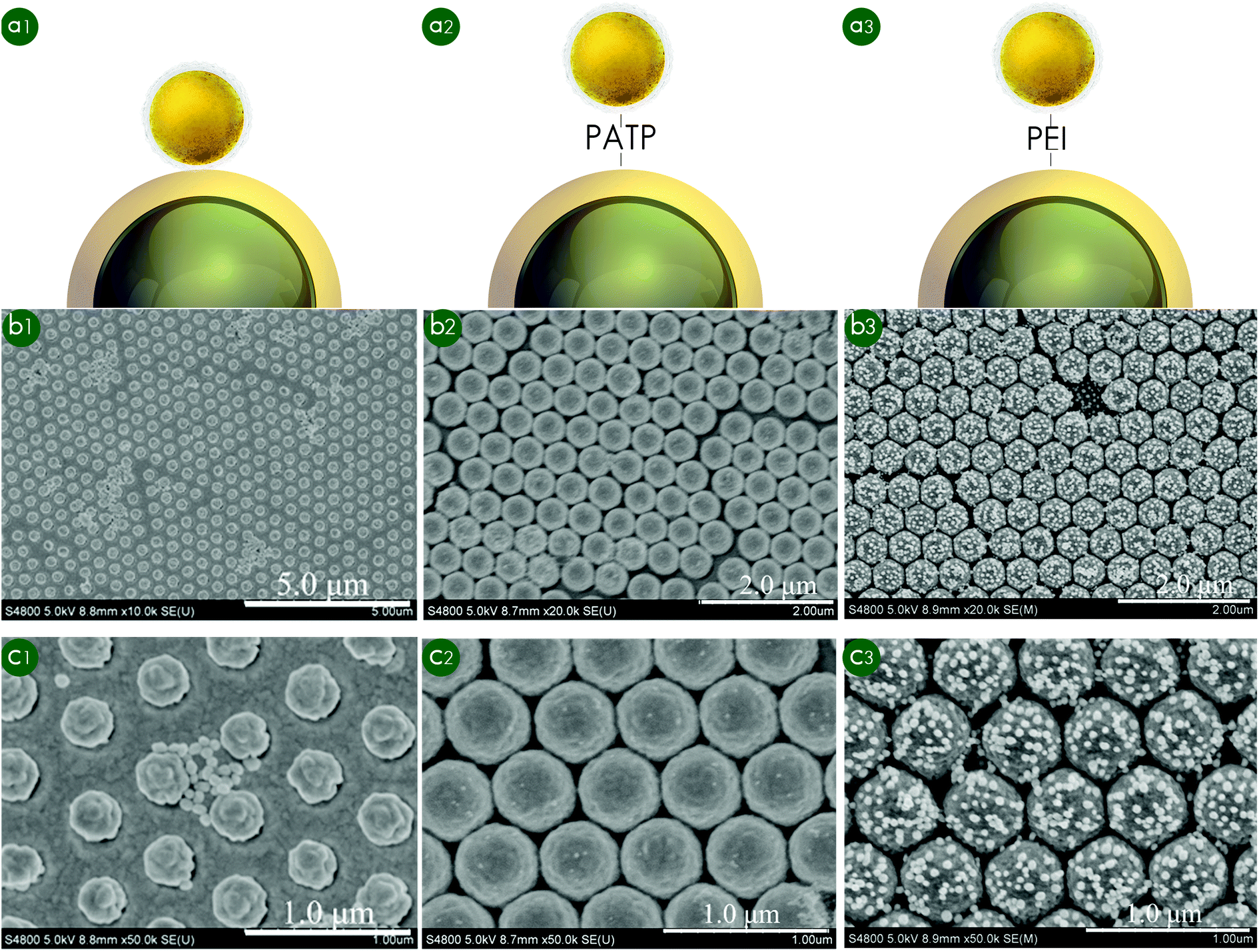 | ||
| Fig. 3 The schematic diagrams, low resolution SEM images and high-resolution SEM images of Au@Ag NPs on AuFON with a physical connection (a1, b1 and c1), small molecule connection (a2, b2 and c2) and polymer connection (a3, b3 and c3). | ||
Polymers provide abundant special chemical groups to improve connection efficiency. Polyetherimide (PEI) can provide thousands of amino groups. This procedure was the same as that using PATP. The AuFON films were cut into pieces and immersed in the PEI ethanol solution. Then the sample was immersed into Au@AgNP solutions to ensure adsorption of Au@AgNPs onto the pendent amino groups, as the other amino groups already remain anchored over the AuFON. The PEI connected particle-AuFON structure is shown in Fig. 3(a3). A large number of Au@Ag NPs were uniformly connected on the AuFON facilitating homogeneous and sensitive SERS detection. Fig. 3(b3) and (c3) show the SEM images of the composite SERS substrate based on PEI connection. It can be seen that the metal sol is uniformly combined with the AuFON structure and the efficiency is obviously improved.
3.2 Optimization of the SERS structure
To improve the SERS performance of the hybrid substrate, its geometry parameters were optimized by adjusting the growth conditions of AuFON and Au@Ag NPs, respectively. It is well known that the hotspots of AuFON mainly locate at the gap between neighboring FON cells. SERS spectra of AuFON with non-etched, 2 min-etched, 3 min-etched, 4 min-etched and 5 min-etched PS beads were acquired using R6G as a Raman probe, as shown in Fig. 4(a). The Raman intensities at 1508 cm−1 for different etching times are shown in Fig. 4(b). All these spectra exhibit good signal to noise ratio; the most intense signal is provided by the 2 min-etched substrate. Slight etching has deepened the gap between the PS beads, facilitating EM field coupling after the Au film deposition. However, too much etching (>3 min) widened the gap, thus weakening the EM field coupling. The plasmonic characteristics of etched substrates were simultaneously calculated with the FDTD method and the results are shown in Fig. S1 in the ESI.† The max |E/E0|2 increases from 325.31 to 593.38 and then decreases to 66.74, 52.06, and 41.29 for the corresponding models, for which the tendency is consistent with measurement results.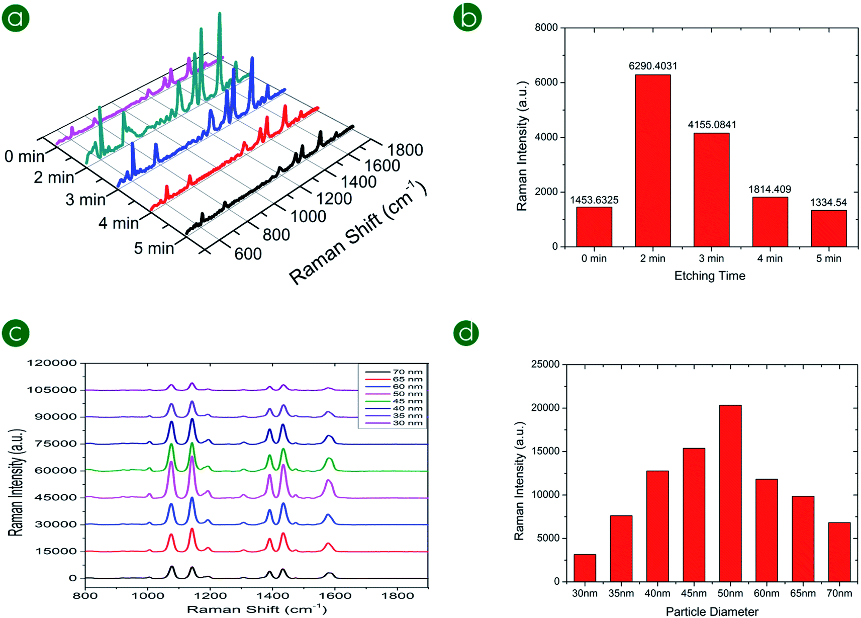 | ||
| Fig. 4 (a) The SERS spectra of NPs on AuFON with different PS bead etching times with probe R6G. (b) The corresponding Raman intensities at a wavelength of 1508 cm−1. (c) The SERS spectra of different diameter NPs on AuFON with probe R6G. (d) The corresponding Raman intensities at wavelength 1508 cm−1. | ||
For further optimization, Au@Ag NPs with various diameters were grafted on the 2 min-etched AuFON for SERS measurements. The parameters of grafted particles are shown in Table S2 in the ESI.† SERS performances were evaluated directly using R6G as a Raman probe. The laser excitation power is 30 mW. The signal intensity first increased (30–50 nm) and then decreased (50–70 nm) with the growth of NP diameter, as shown in Fig. 4(c). The corresponding Raman intensities at 1508 cm−1 are shown in Fig. 4(d). The structure grafted with 50 nm NPs exhibited the best performance. The FDTD calculation shows that the EM field enhancement of the Au@Ag NPs increased with the growth of the particle diameter, as shown in Fig. S2 in the ESI.† However, it is harder to firmly immobilize the particles on the surface with the growth of NP diameter. Moreover, the density of hotspots on AuFON decreased with the growth of NP diameter. In summary, Au@Ag NPs with diameter of 50 nm and AuFON with PS beads etched for 2 min were employed herein to construct the particle-AuFON configuration.
3.3 SERS measurements
To evaluate the SERS performance of the hybrid substrate, Raman spectra were obtained from the as-fabricated AuFON, Au@AgNPs, and particle-AuFON structure, as shown in Fig. 5. R6G in concentrations ranging from 10−10 to 10−4 M was utilized as the Raman probe. The R6G solution was dropped onto the AuFON and hybrid substrate directly and dried in the air for SERS measurements. For the Au@Ag NPs, R6G was mixed into the sol at a certain concentration and dried for SERS measurements. The detection limit is defined according to the principle that the signal is valid when the signal/noise is greater than 3![[thin space (1/6-em)]](https://www.rsc.org/images/entities/char_2009.gif) :1. Under these conditions, the detection limits were 10−8 M, 10−8 M, and 10−10 M for AuFON, Au@AgNPs, and particle-AuFON structure, respectively. The detection limit of the particle-AuFON configuration was about 2 orders of magnitude better than those of AuFON and Au@Ag NPs, indicating that the hybridization method facilitates the improvement of SERS sensitivity. Detailed Raman intensities in the wavelength range of 1475 cm−1 to 1550 cm−1 are shown in Fig. S3.†
:1. Under these conditions, the detection limits were 10−8 M, 10−8 M, and 10−10 M for AuFON, Au@AgNPs, and particle-AuFON structure, respectively. The detection limit of the particle-AuFON configuration was about 2 orders of magnitude better than those of AuFON and Au@Ag NPs, indicating that the hybridization method facilitates the improvement of SERS sensitivity. Detailed Raman intensities in the wavelength range of 1475 cm−1 to 1550 cm−1 are shown in Fig. S3.†
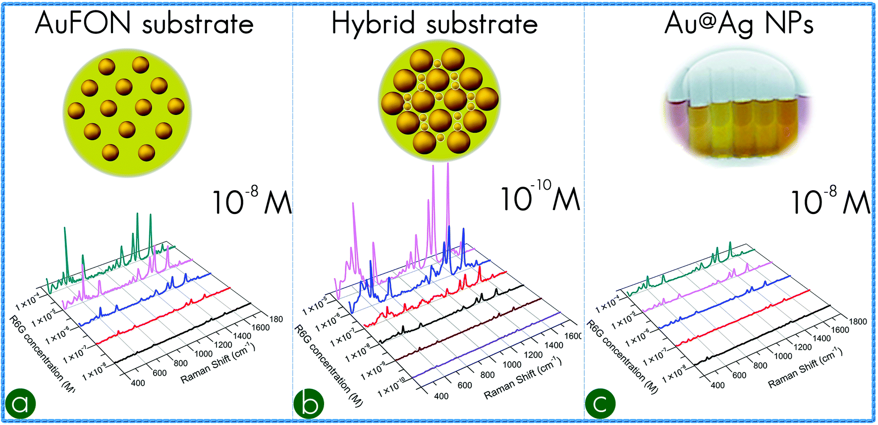 | ||
| Fig. 5 (a–c) Raman spectra obtained from the Au@Ag NPs, AuFON and particle-AuFON structures, respectively, with probe R6G. The concentrations of R6G are 10−4, 10−5, 10−6, 10−7, 10−8, 10−9, and 10−10 M. The detection limit of the hybrid configuration is 2 orders lower than those of than AuFON and Au@Ag NPs. | ||
3.4 Uniformity, repeatability and stability of the particle-AuFON configuration
Most of the reported SERS substrates, created by solution synthesis or nano-manufactory, can provide sufficient enhancement ability, sometimes capable of single molecule detection. Although many of these have offered exceptional electromagnetic enhancement, the durability and reusability of substrates have not always been acceptable for practical applications. Herein, controlled experiments were conducted to evaluate the uniformity, repeatability and stability of the hybrid substrate using PATP as a Raman probe. The hybrid SERS substrates were immersed in 10−6 M PATP solution for 2 hours and dried for SERS measurements. To study its uniformity, SERS spectra were obtained on 20 sites of the same sample. The locations of these sites are inserted in Fig. S4 in the ESI.† SERS spectra acquired from these sites were all similar, as shown in Fig. 6(a). A p-color image was obtained by extracting the signal intensities at the wavelength of 1076 cm−1 and is shown in Fig. 6(b). Its similar red colors indicated the good uniformity of the hybrid substrate. The RSD of the Raman intensity was 10.36%, which meets the requirement for practical application. To validate its repeatability, five spectra were acquired from three samples out of three batches, separately, as shown in Fig. 6(c). Average intensity of each batch is shown in Fig. 6(d): it changes 6.7% and 9.8% among these three batches, which indicates that the SERS signals were repeatable under strict experimental control. To test the stability of the hybrid substrate, spectra were obtained from the same substrate after fabrication, a month later, and three months later, as shown in Fig. 6(e). The intensity of the SERS signals decreased 5.6% after a month and changed 2.7% after two months, as shown in Fig. 6(f). These measurements demonstrate that the hybrid SERS substrate has the potential to meet the demand of practical applications.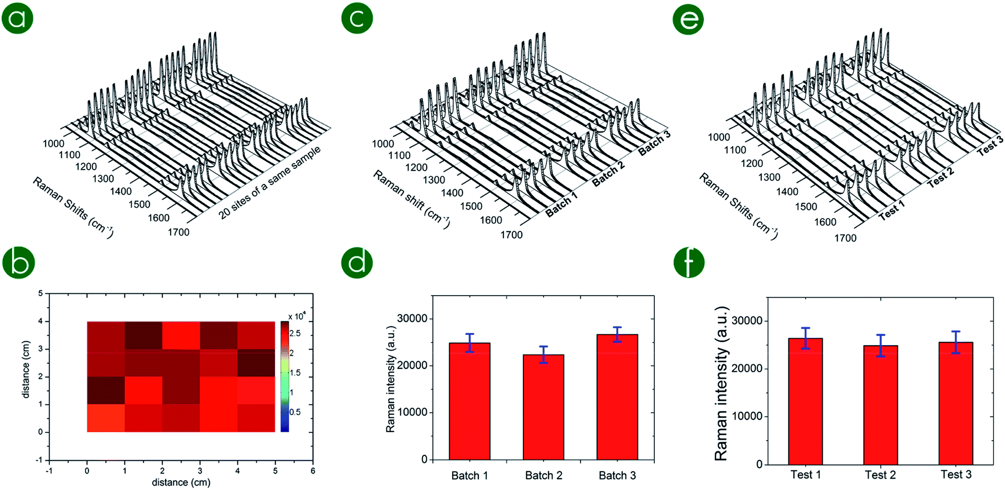 | ||
| Fig. 6 (a and b) The uniformity, (c and d) repeatability and (e and f) stability measurements of the hybrid configuration. | ||
3.5 Plasmonic characteristic
To investigate the surface plasmonic characteristics, FDTD method was employed for visualization of the EM field. When an Au@Ag NP was introduced onto the plane film, a hotspot was created at the gap, as shown in Fig. 7. When Au@Ag NPs were introduced onto the corrugated film, one-point or two-point contact may occur, as shown in Fig. 7(a1) and (a2). The diameter of the nanoparticle was chosen to be 50 nm, the same as the best candidate in the experimental section. Dielectric constant distributions of models are shown in Fig. 7(b1) and (b2). The calculated EM field distributions in the XY, XZ and YZ planes are shown in Fig. 7(c1, c2), (d1, d2) and (e1, e2), respectively. The scale bar for the EM field distribution was log|E/E0|2. For the single point contact model, the EM field was concentrated at the gap between the Au@Ag NP and the AuFON with an enhancement of 31.2-fold, as shown in Fig. 7(c1)–(e1). For the two-point contact model, two hotspots were created at the two new gaps and further coupled with the original hotspot of the AuFON, resulting in an EM field enhancement of 2391.6, as shown in Fig. 7(c2)–(e2). In Fig. 7(c2), z = 279 nm, at which point the position of the contact between the particle and the AuFON was monitored. Distributions of dielectric constants and electromagnetic fields of a single NP on silicon and gold substrates are shown in Fig. S5.† These simulation results indicate the corrugated film has great advantage over flat films.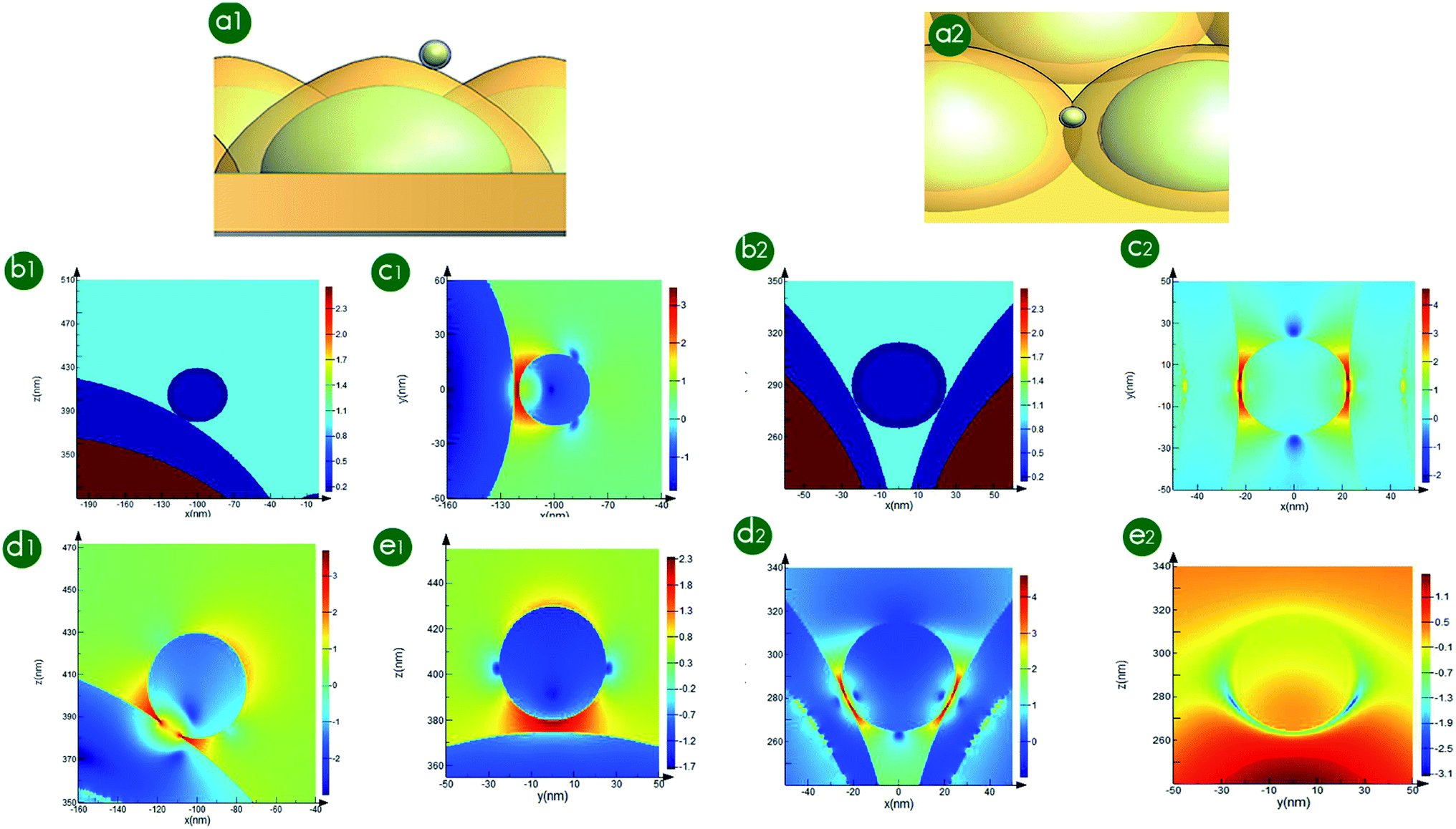 | ||
| Fig. 7 (a1 and a2) Models of single point and two-point contact. (b1 and b2) Dielectric constant distributions of these models. (c1 and c2) Calculated EM field distributions in XY plane. (d1 and d2) Calculated EM field distributions in XZ plane. (e1 and e2) Calculated EM field distributions in YZ plane. | ||
Furthermore, nanoparticles may exist in the form of a cluster. The schematic diagram of contact between an Au@AgNP cluster (3 particles) and the AuFON structure is shown in Fig. 8, where the diameter of the NPs is 50 nm. Fig. 8(b) gives the simulation results for the local dielectric constant at the combination position and Fig. 8(c)–(e) show the substrate EM field distributions in the XY plane, the XY plane and the YZ plane, respectively. Since the Au@AgNPs are arranged on a curved surface, the three NPs are not at the same height. Therefore, in the horizontal plane of XY, the electromagnetic field intensity of each Au@AgNPs gap position is quite different, as shown in Fig. 8(c). New hotspots were produced in the contact position between Au@AgNPs sol and AuFON structure. Meanwhile, in the gaps between Au@AgNPs sol, the SERS hotspot intensity was also greatly enhanced due to EM field coupling.
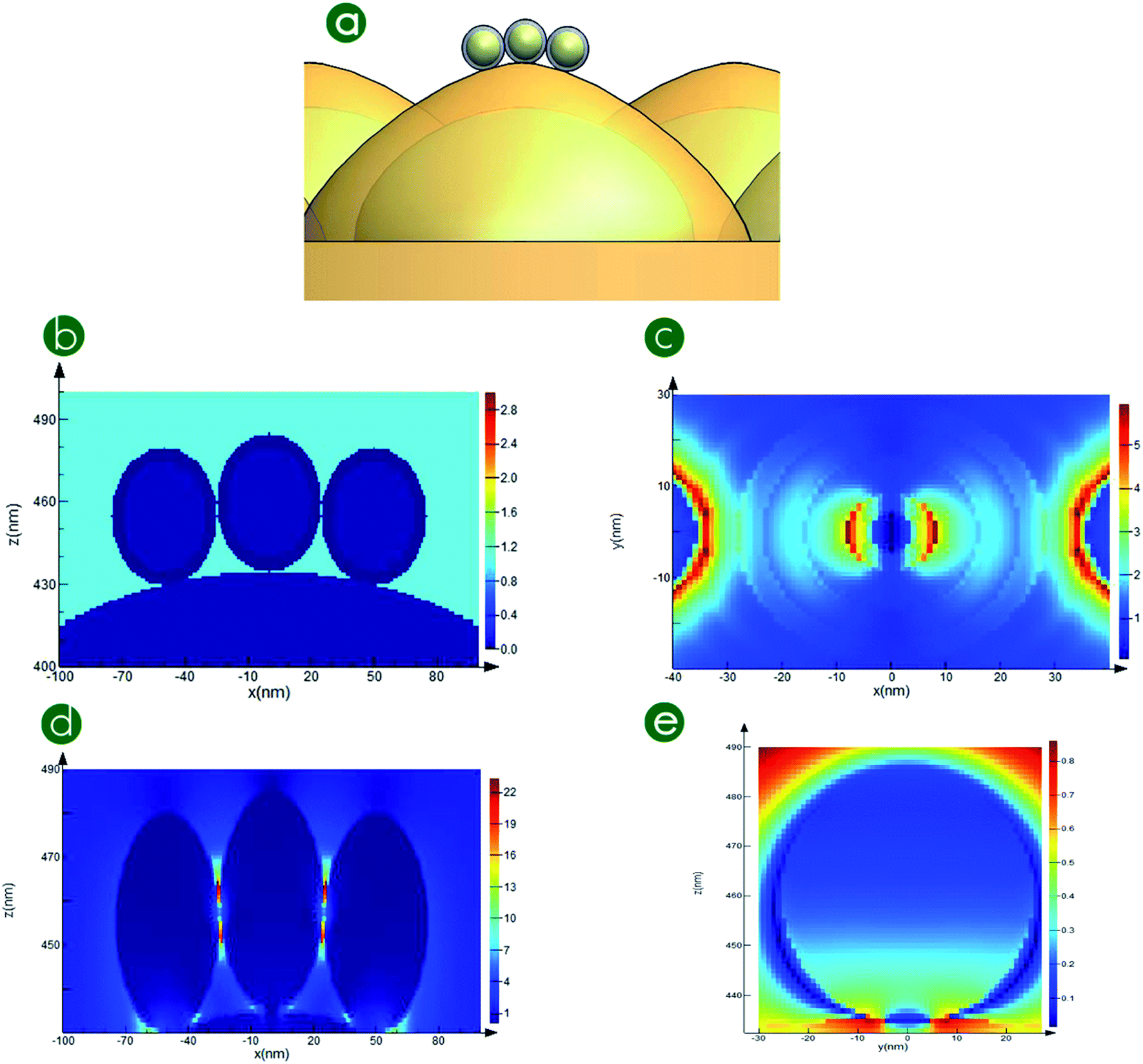 | ||
| Fig. 8 (a) The schematic diagram and EM field distribution of Au@Ag NPs cluster on AuFON. (b) The local dielectric constants at the combination position. (c–e) The distributions of the EM field of the substrate in the XY plane, XY plane and YZ plane, respectively. | ||
Compared with Au@AgNPs or clusters on Si or Au film substrates, the EM field enhancement effect of Au@AgNPs on corrugated film is great. Furthermore, nanoparticle clusters show enhancement compared with single particles. The calculations of plasmatic characteristics showed that the construction of the particle-AuFON configuration not only introduces a great many hotspots, but also couples with the original ones, improving the intensity and densifying the distribution of the hotspots.
3.6 Melamine detection
Melamine is well-known as an adulterant in milk products (e.g., infant formula) to supplement their apparent protein content with its rich nitrogen content (66% by mass). It is a hard task to distinguish melamine in milk. SERS technique is a good candidate for rapid and sensitive melamine detection, for it is able to distinguish the intrinsic Raman spectrum of melamine. The Raman vibration band distribution of melamine is shown in Table S3 in the ESI.† The main peak locates in the wavelength range from 670 cm−1 to 710 cm−1.To test the feasibility of the SERS technique, melamine solution with concentrations ranging from 10−8 M to 10−4 M were prepared and dropped on the hybrid substrate. SERS spectra were acquired after the solution dried, as shown in Fig. 9(a). Herein, water was used as the negative signal reference. From the curve detail shown in Fig. 9(b), the SERS signal intensities decreased with the dilution of melamine concentration, with a detection limit of 10 nM (1.2 ppb), which is much lower than the maximum limit of melamine in infant formula (1 ppm) legislated by the governments of both the United States and China.
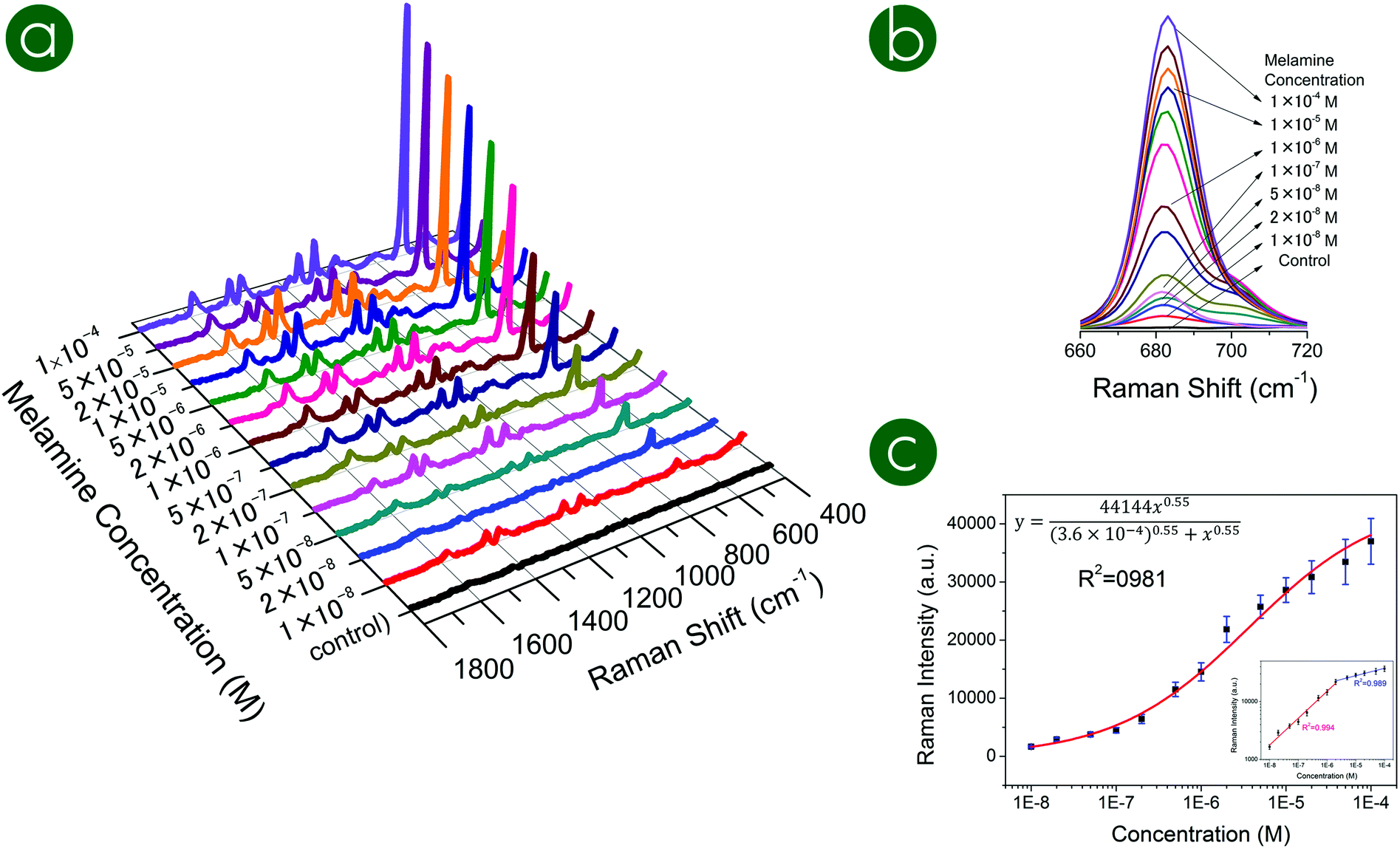 | ||
| Fig. 9 (a) SERS spectra of different concentrations of melamine on the hybrid substrate. (b) SERS peaks at wavelengths 670 cm−1 to 710 cm−1. (c) The fitting calibration curve plotted between the SERS intensity at 681 cm−1 and the concentration of melamine. | ||
To quantitatively detect melamine, a calibration curve was plotted between the SERS intensity at the wavelength of 681 cm−1 and the concentration of melamine by fitting Hill's equation as shown in Fig. 9(c). All the data were the average of five measurements with error bars. The fitting equation was y = 44144x0.55/((3.6 × 10−4)0.55 + x0.55) with a correlation coefficient of 0.98, where y is the Raman intensity and x is the concentration of melamine. Two linear equations were obtained by fitting log–log values and the equilibrium constant was calculated to be 3.6 × 10⁻⁶. The fitting equations were calculated to be as follows:
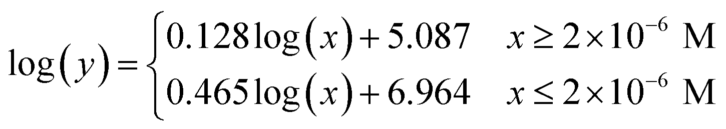
The correlation coefficients were 0.989 and 0.994, respectively, which indicated the potential of the hybrid substrate in quantitative measurements.
4. Conclusions
In this paper, we reported the optimization method and SERS performance of a hybrid substrate fabricated by immobilizing the Au@Ag NPs onto the AuFON substrate. Polymer was employed as a binder to connect the NPs onto the AuFON for a firm, dense and stable binding with whole process oscillation. The parameters of the hybrid substrate were optimized, mainly focusing on the PS bead etching time and the diameter of the NPs. AuFON with PS beads etched for 2 min and NPs with a diameter of 50 nm were shown to be the best options for SERS measurements. This construction provides a detection limit of 1 × 10⁻¹⁰ M, which was about 100-fold improvement compared to single AuFON or Au@Ag NPs. The uniformity, repeatability, and stability of the substrate were also tested, demonstrating its potential in practical SERS-based applications. To visualize the hotspots, the EM field distribution was calculated by the FDTD method. Coupling models were built and calculated in which additional hotspots were created at the junctions between the particle and the corrugated film and created hotspots coupled to the original ones. Thus, both the intensity and density of the hotspots were improved, facilitating signal enhancement. The hybrid substrate was used in the sensing of melamine by its intrinsic spectrum. The detection limit was 10 nM (1.2 ppb), which was much lower than the maximum limit of melamine in infant formula (1 ppm) legislated by the governments of both the United States and China. A calibration curve was plotted between the SERS intensity at the wavelength of 681 cm−1 and the melamine concentrations by fitting Hill's equation for quantitative detection with a correlation coefficient of 0.98. Two linear equations were obtained by fitting log–log values, with correlation coefficients of 0.989 and 0.994.Conflicts of interest
There are no conflicts to declare.Acknowledgements
This study was supported by the National Natural Science Foundation of China (Grant no. 51605486, 51705527).Notes and references
- V.-D. Tuan, Surface-enhanced Raman spectroscopy using metallic nanostructures, TrAC, Trends Anal. Chem., 1998, 17(8–9), 557–582 Search PubMed.
- R. Gordon, D. Sinton, K. L. Kavanagh and A. G. Brolo, A new generation of sensors based on extraordinary optical transmission, Acc. Chem. Res., 2008, 41(8), 1049–1057 CrossRef CAS.
- W. Wu, M. Hu, F. S. Ou, Z. Li and R. S. Williams, Cones fabricated by 3D nanoimprint lithography for highly sensitive surface enhanced Raman spectroscopy, Nanotechnology, 2010, 21(25), 255502 CrossRef.
- P. Camden Jon, A. Dieringer Jon, Z. Jing and P. Van Duyne Richard, Controlled Plasmonic Nanostructures for Surface-Enhanced Spectroscopy and Sensing, Acc. Chem. Res., 2008, 41(12), 1653–1661 CrossRef CAS PubMed.
- G. Greeneltch Nathan, G. Blaber Martin, H. Anne-Isabelle, C. Schatz George and P. Van Duyne Richard, Immobilized Nanorod Assemblies: Fabrication and Understanding of Large Area Surface-Enhanced Raman Spectroscopy Substrates, Anal. Chem., 2013, 85(4), 2297–2303 CrossRef CAS.
- L. Haynes Christy, D. Mcfarland Adam and P. V. Duyne Richard, Surface-Enhanced Raman Spectroscopy, Anal. Chem., 2005, 77(17), 338 A–346 A CrossRef.
- K. Ma, M. Yuen Jonathan, C. Shah Nilam, T. Walsh Joseph, R. Glucksberg Matthew and P. Van Duyne Richard, In Vivo, Transcutaneous Glucose Sensing Using Surface-Enhanced Spatially Offset Raman Spectroscopy: Multiple Rats, Improved Hypoglycemic Accuracy, Low Incident Power, and Continuous Monitoring for Greater than 17 Days, Anal. Chem., 2011, 83(23), 9146–9152 CrossRef CAS.
- E. Kreno Lauren, K. Leong, K. Farha Omar, A. Mark, P. Van Duyne Richard and T. Hupp Joseph, Metal–Organic Framework Materials as Chemical Sensors, Chem. Rev., 2011, 112(2), 1105–1125 CrossRef PubMed.
- M. Fan, F. Cheng, C. Wang, Z. Gong, C. Tang, C. Man and A. G. Brolo, SERS optrode as a “fishing rod” to direct pre-concentrate analytes from superhydrophobic surfaces, Chem. Commun., 2015, 51(10), 1965–1968 RSC.
- J. Haes Amanda, J. Zhao, S. Zou, S. Own Christopher, D. Marks Laurence, C. Schatz George and P. Van Duyne Richard, Solution-Phase, Triangular Ag Nanotriangles Fabricated by Nanosphere Lithography, J. Phys. Chem. B, 2005, 109(22), 11158–11162 CrossRef CAS.
- J. Haes Amanda, S. Zou, C. Schatz George and P. Van Duyne Richard, A Nanoscale Optical Biosensor: The Long Range Distance Dependence of the Localized Surface Plasmon Resonance of Noble Metal Nanoparticles, J. Phys. Chem. B, 2003, 108(1), 109–116 CrossRef.
- J. Haes Amanda, S. Zou, C. Schatz George and P. Van Duyne Richard, Nanoscale Optical Biosensor: Short Range Distance Dependence of the Localized Surface Plasmon Resonance of Noble Metal Nanoparticles, J. Phys. Chem. B, 2004, 108(22), 6961–6968 CrossRef.
- L. Haynes Christy, D. Mcfarland Adam, T. Smith Matthew, C. Hulteen John and P. Van Duyne Richard, Angle-Resolved Nanosphere Lithography: Manipulation of Nanoparticle Size, Shape, and Interparticle Spacing, J. Phys. Chem. B, 2002, 106(8), 1898–1902 CrossRef.
- L. Haynes Christy, D. Mcfarland Adam, L. Zhao, P. Van Duyne Richard, C. Schatz George, L. Gunnarsson, J. Prikulis, B. Kasemo and M. Käll, Nanoparticle Optics: The Importance of Radiative Dipole Coupling in Two-Dimensional Nanoparticle Arrays, J. Phys. Chem. B, 2003, 107(30), 7337–7342 CrossRef.
- L. Haynes Christy and P. Van Duyne Richard, Nanosphere Lithography: A Versatile Nanofabrication Tool for Studies of Size-Dependent Nanoparticle Optics, J. Phys. Chem. B, 2001, 105(24), 5599–5611 CrossRef.
- M. Hicks Erin, X. Zhang, S. Zou, L. Olga, G. Spears Kenneth, C. Schatz George and P. Van Duyne Richard, Plasmonic Properties of Film over Nanowell Surfaces Fabricated by Nanosphere Lithography, J. Phys. Chem. B, 2005, 109(47), 22351–22358 CrossRef CAS.
- C. Hulteen John, A. Treichel David, T. Smith Matthew, L. Duval Michelle, R. Jensen Traci and P. Van Duyne Richard, Nanosphere Lithography: Size-Tunable Silver Nanoparticle and Surface Cluster Arrays, J. Phys. Chem. B, 1999, 103(19), 3854–3863 CrossRef.
- R. Jensen Traci, D. Malinsky Michelle, L. Haynes Christy and P. Van Duyne Richard, Nanosphere Lithography: Tunable Localized Surface Plasmon Resonance Spectra of Silver Nanoparticles, J. Phys. Chem. B, 2000, 104(45), 10549–10556 CrossRef.
- S. L. Hennigan, J. D. Driskell, N. Ferguson-Noel, R. A. Dluhy, Y. Zhao, R. A. Tripp and D. C. Krause, Detection and differentiation of avian mycoplasmas by surface-enhanced Raman spectroscopy based on a silver nanorod array, Appl. Environ. Microbiol., 2012, 78(6), 1930–1935 CrossRef CAS PubMed.
- J. L. Abell, J. M. Garren and Y. Zhao, Dynamic rastering surface-enhanced Raman scattering (SERS) measurements on silver nanorod substrates, Appl. Spectrosc., 2011, 65(7), 734–740 CrossRef CAS.
- Q. Zhou, Y. He, J. Abell, Z. Zhang and Y. Zhao, Surface-enhanced Raman scattering from helical silver nanorod arrays, Chem. Commun., 2011, 47(15), 4466–4468 RSC.
- Y. P. Zhao, S. B. Chaney, S. Shanmukh and R. A. Dluhy, Polarized surface enhanced Raman and absorbance spectra of aligned silver nanorod arrays, J. Phys. Chem. B, 2006, 110(7), 3153–3157 CrossRef CAS.
- J. G. Fan and Y. P. Zhao, Gold-coated nanorod arrays as highly sensitive substrates for surface-enhanced raman spectroscopy, Langmuir, 2008, 24(24), 14172–14175 CrossRef CAS.
- S. Shanmukh, L. Jones, J. Driskell, Y. Zhao, R. Dluhy and R. A. Tripp, Rapid and sensitive detection of respiratory virus molecular signatures using a silver nanorod array SERS substrate, Nano Lett., 2006, 6(11), 2630–2636 CrossRef CAS.
- J. Zhang, X. Zhang, C. Lai, H. Zhou and Y. Zhu, Silver-decorated aligned CNT arrays as SERS substrates by high temperature annealing, Opt. Express, 2014, 22(18), 21157–21166 CrossRef.
- M. M. Arnob, F. Zhao, J. Zeng, G. M. Santos, M. Li and W. C. Shih, Laser rapid thermal annealing enables tunable plasmonics in nanoporous gold nanoparticles, Nanoscale, 2014, 6(21), 12470–12475 RSC.
- X. Sun and H. Li, Gold nanoisland arrays by repeated deposition and post-deposition annealing for surface-enhanced Raman spectroscopy, Nanotechnology, 2013, 24(35), 355706 CrossRef.
- X. Hu, T. Wang and S. Dong, Thermal annealing of Au nanorod self-assembled nanostructured materials: morphology and optical properties, J. Colloid Interface Sci., 2007, 316(2), 947–953 CrossRef CAS.
- H. Zou, S. Wu and J. Shen, Polymer/silica nanocomposites: preparation, characterization, properties, and applications, Chem. Rev., 2008, 108(9), 3893–3957 CrossRef CAS.
- M. D. Porter, R. J. Lipert, L. M. Siperko, G. Wang and R. Narayanan, SERS as a bioassay platform: fundamentals, design, and applications, Chem. Soc. Rev., 2008, 37(5), 1001–1011 RSC.
- H. Chen, Y. Wang, S. Dong and E. Wang, An approach for fabricating self-assembled monolayer of Ag nanoparticles on gold as the SERS-active substrate, Spectrochim. Acta, Part A, 2006, 64(2), 343–348 CrossRef.
- J. F. Li, Y. F. Huang, Y. Ding, Z. L. Yang, S. B. Li, X. S. Zhou, F. R. Fan, W. Zhang, Z. Y. Zhou, D. Y. Wu, B. Ren, Z. L. Wang and Z. Q. Tian, Shell-isolated nanoparticle-enhanced Raman spectroscopy, Nature, 2010, 464(7287), 392–395 CrossRef CAS.
- E. Chung, R. Gao, J. Ko, N. Choi, D. W. Lim, E. K. Lee, S. I. Chang and J. Choo, Trace analysis of mercury(II) ions using aptamer-modified Au/Ag core-shell nanoparticles and SERS spectroscopy in a microdroplet channel, Lab Chip, 2013, 13(2), 260–266 RSC.
- A. K. Samal, L. Polavarapu, S. Rodal-Cedeira, L. M. Liz-Marzan, J. Perez-Juste and I. Pastoriza-Santos, Size tunable Au@Ag core–shell nanoparticles: synthesis and surface-enhanced Raman scattering properties, Langmuir, 2013, 29(48), 15076–15082 CrossRef CAS.
- H. Zhang, H. Harpster Mark, H. J. Park, A. Johnson Patrick and W. C. Wilson, Surface-Enhanced Raman Scattering Detection of DNA Derived from the West Nile Virus Genome Using Magnetic Capture of Raman-Active Gold Nanoparticles, Anal. Chem., 2010, 83(1), 254–260 CrossRef.
- Q. An, P. Zhang, J. M. Li, W. F. Ma, J. Guo, J. Hu and C. C. Wang, Silver-coated magnetite-carbon core-shell microspheres as substrate-enhanced SERS probes for detection of trace persistent organic pollutants, Nanoscale, 2012, 4(16), 5210–5216 RSC.
- D. K. Lim, K. S. Jeon, J. H. Hwang, H. Kim, S. Kwon, Y. D. Suh and J. M. Nam, Highly uniform and reproducible surface-enhanced Raman scattering from DNA-tailorable nanoparticles with 1 nm interior gap, Nat. Nanotechnol., 2011, 6(7), 452–460 CrossRef CAS.
- D. K. Lim, K. S. Jeon, H. M. Kim, J. M. Nam and Y. D. Suh, Nanogap-engineerable Raman-active nanodumbbells for single-molecule detection, Nat. Mater., 2010, 9(1), 60–67 CrossRef CAS.
- J. H. Lee, J. M. Nam, K. S. Jeon, D. K. Lim, H. Kim, S. Kwon, H. Lee and Y. D. Suh, Tuning and Maximizing the Single-Molecule Surface-Enhanced Raman Scattering from DNA-Tethered Nanodumbbells, ACS Nano, 2012, 6(11), 9574–9584 CrossRef CAS.
- J. F. Li, J. R. Anema, Y. C. Yu, Z. L. Yang, Y. F. Huang, X. S. Zhou, B. Ren and Z. Q. Tian, Core–shell nanoparticle based SERS from hydrogen adsorbed on a rhodium(111) electrode, Chem. Commun., 2011, 47(7), 2023–2025 RSC.
- J. F. Li, S. Y. Ding, Z. L. Yang, M. L. Bai, J. R. Anema, X. Wang, A. Wang, D. Y. Wu, B. Ren, S. M. Hou, T. Wandlowski and Z. Q. Tian, Extraordinary enhancement of Raman scattering from pyridine on single crystal Au and Pt electrodes by shell-isolated Au nanoparticles, J. Am. Chem. Soc., 2011, 133(40), 15922–15925 CrossRef CAS.
- L. J. Feng, T. X. Dong, L. S. Bo, R. Anema Jason, Y. Z. Lin, Y. Ding, W. Y. Fei, Z. Y. Ming, C. Q. Zhen, B. Ren, W. Z. Lin and Z. Q. Tian, Surface analysis using shell-isolated nanoparticle-enhanced Raman spectroscopy, Nat. Protoc., 2013, 8(1), 52–65 CrossRef.
- L. Jian-Feng, S.-Y. Ding, Z.-L. Yang, B. Mei-Lin, R. Anema Jason, X. Wang, A. Wang, D.-Y. Wu, B. Ren, H. Shi-Min, W. Thomas and Z.-Q. Tian, Extraordinary Enhancement of Raman Scattering from Pyridine on Single Crystal Au and Pt Electrodes by Shell-Isolated Au Nanoparticles, J. Am. Chem. Soc., 2011, 133(40), 15922–15925 CrossRef PubMed.
- L. Jian-Feng, Z.-L. Yang, B. Ren, L. Guo-Kun, P.-P. Fang, Yu-X. Jiang, D.-Y. Wu and Z.-Q. Tian, Surface-Enhanced Raman Spectroscopy Using Gold-Core Platinum-Shell Nanoparticle Film Electrodes: Toward a Versatile Vibrational Strategy for Electrochemical Interfaces, Langmuir, 2006, 22(25), 10372–10379 CrossRef PubMed.
- X. Li, S. Zhang, Z. Yu and T. Yang, Surface-enhanced Raman spectroscopic analysis of phorate and fenthion pesticide in apple skin using silver nanoparticles, Appl. Spectrosc., 2014, 68(4), 483–487 CrossRef CAS.
- X. Liu, C. Zong, K. Ai, W. He and L. Lu, Engineering natural materials as surface-enhanced Raman spectroscopy substrates for in situ molecular sensing, ACS Appl. Mater. Interfaces, 2012, 4(12), 6599–6608 CrossRef CAS.
- K. Kim, H. B. Lee and K. S. Shin, Surface-enhanced Raman scattering characteristics of nanogaps formed by a flat Ag substrate and spherical Pt nanoparticles, Spectrochim. Acta, Part A, 2013, 100, 10–14 CrossRef CAS.
- K. Kim, J. Y. Choi and K. S. Shin, Raman scattering characterization of 1,4-phenylenediisocyanide in Au–Au and Ag–Au nanogaps, Spectrochim. Acta, Part A, 2013, 100, 3–9 CrossRef CAS.
- J. Wang, X. Wu, R. Xiao, P. Dong and C. Wang, Performance-Enhancing Methods for Au Film over Nanosphere Surface-Enhanced Raman Scattering Substrate and Melamine Detection Application, PLoS One, 2014, 9(6), e97976 CrossRef.
- C. Wang, X. Wu, P. Dong, J. Chen and R. Xiao, Hotspots engineering by grafting Au@Ag core-shell nanoparticles on the Au film over slightly etched nanoparticles substrate for on-site paraquat sensing, Biosens. Bioelectron., 2016, 86, 944–950 CrossRef CAS.
- C. Wang, X. Wu, P. Dong, J. Wang, D. Di, J. Chen and H. Wang, Diversification of nanostructure morphology by modifying angle-resolved heterogeneous shadow mask, J. Nanosci. Nanotechnol., 2013, 13(12), 8259–8265 CrossRef CAS.
- D. I. Di, P. Dong, C. Wang, J. Chen, J. Wang, H. Wang, X. Wu and S. Li, High-ordered and ultra-sensitive particle-in-bowl metallic arrays for surface enhanced raman spectroscopy, Nano, 2014, 1450050 CrossRef.
- J. Chen, P. Dong, D. Di, C. Wang, H. Wang, J. Wang and X. Wu, Controllable fabrication of 2D colloidal-crystal films with polystyrene nanospheres of various diameters by spin-coating, Appl. Surf. Sci., 2013, 270(1), 6–15 CrossRef CAS.
- E. D. Palik, Handbook of Optical Constants of Solids, Academic Press, 1985 Search PubMed.
Footnote |
| † Electronic supplementary information (ESI) available. See DOI: 10.1039/c9ra02371b |
| This journal is © The Royal Society of Chemistry 2019 |