 Open Access Article
Light induced reversible structuring of photosensitive polymer films†
Joachim Jelken and
Svetlana Santer *
*
Institute of Physics and Astronomy, University of Potsdam, 14476 Potsdam, Germany. E-mail: santer@uni-potsdam.de
First published on 28th June 2019
Abstract
In this paper we report on photoswitchable polymer surfaces with dynamically and reversibly fluctuating topographies. It is well known that when azobenzene containing polymer films are irradiated with optical interference patterns the film topography changes to form a surface relief grating. In the simplest case, the film shape mimics the intensity distribution and deforms into a wave like, sinusoidal manner with amplitude that may be as large as the film thickness. This process takes place in the glassy state without photo-induced softening. Here we report on an intriguing discovery regarding the formation of reliefs under special illumination conditions. We have developed a novel setup combining the optical part for creating interference patterns, an AFM for in situ acquisition of topography changes and diffraction efficiency signal measurements. In this way we demonstrate that these gratings can be “set in motion” like water waves or dunes in the desert. We achieve this by applying repetitive polarization changes to the incoming interference pattern. Such light responsive surfaces represent the prerequisite for providing practical applications ranging from conveyer or transport systems for adsorbed liquid objects and colloidal particles to generation of adaptive and dynamic optical devices.
Introduction
Designing programmable polymer substrates is an active and growing field of research, continuously pushed by many branches of nanotechnology seeking unprecedented and ever more efficient solutions for developing novel types of sensors, strategies for self-healing integrated structures, optical information storage, solutions for creating adaptable and dynamic optical devices (auto focusing lenses, DFB lasers, diffractive thin films, diffusers and directional reflectors) or hybrid bio-electro-mechanical systems.1–11 In even more exotic applications one utilizes dynamically switchable surfaces for controlling the adhesion and thus the position of adsorbed particles (a gecko “in reverse”), or for moving and handling small amounts of liquid within micrometer dimensions such as microfluidic chambers, channels or surfaces that act as microarrays for droplet deposition and screening.1,12–15 In a general sense, programmable polymer substrates may be defined as systems the surface topography and morphology of which, including local surface energy and ordering, can be switched between distinct states by applying external stimuli such as electrical fields, temperature or light.16–18 Photo-switchable surfaces offer greater simplicity and convenience in manipulation, since light as an external stimulus can be tuned and controlled spatio-temporally without undesired contact with electrodes, wires or heating elements.19–23 One of the strategies to render a polymer photo-responsive is to modify it with photo-reactive groups among which azobenzenes are the most common. Azobenzene containing polymers belong to a class of functional materials exhibiting a strong mechanical response upon applying external radiation fields. Although the radiation only acts on the photo-sensitive azobenzene moieties by inducing trans–cis isomerization and thus configurational changes, as side groups in a polymer chains they can affect the system as a whole. Such materials have extensively been studied and were proposed for the construction of holographic gratings and optical data storage devices.10 Very peculiar phenomena are obtained when azobenzene modified physisorbed polymer films or the even more exotic polymer brushes are exposed to irradiation exhibiting interference patterns (IP).24–32 Following the IP's periodicity either with respect to intensity or polarization distribution, the polymer topography is modulated into a wave like form with period equal to optical one.33–36 The mechanism of SRG formation is related to the generation of strong, internal opto-mechanical stresses. Since the polymer material is in a glassy state, the opto-mechanical stresses needed for the deformation of mechanically stable polymer films (Young modulus of several GPa) must be quite high of 100 MPa up to ∼1 GPa, as was recently shown.37–40 The process can be viewed as follows: under irradiation inducing cyclic trans–cis–trans isomerization,41 the azobenzene molecules rotate and re-orient perpendicularly to the electrical field vector (formation of bulk birefringence grating) causing a re-orientation of the polymer backbones to which they are attached. This creates local gradients in internal stresses within the polymer material, varying with the distribution of the interference pattern and thus induces a viscoplastic deformations of the solid material (formation of topographical grating).42–47 In fact, the inscribed SRG topography is stable over years at room temperature and can be erased only by further intense treatment such as either irradiation with a circularly polarized beam48 or by heating49 the polymer sample above the glass transition temperature.Usually the dynamics of the SRG formation is probed by measuring the changing diffraction efficiency of the formed grating. Here a probe beam not affecting the azobenzene moieties is focused on the relief structure and the change in intensity of the first order diffraction peak is recorded as a function of time. The surface grating and the birefringent grating contribute to the signal and it is hard to separate these two components.50–52 Another approach is to directly measure the change in the SRG using an atomic force microscope (AFM).39,53–55 The drawback of the latter methodology is that there will be no information obtained about the orientation process in the bulk polymer. Here we present a novel set-up which combines these two approaches.
An AFM is integrated into a two beam interference set-up generating the interference pattern. This allows the in situ acquisition of surface topography changes. At the same time the diffraction efficiency (DE) signal is measured to obtain information about the bulk birefringence. Integrating a delay stage into the two beam setup allows controllable spatio-temporal shifts of the interference pattern, which locally appears as a redistribution of the electrical field vector. In this way gradual shifts or even more dynamic fluctuations in the polymer topography and the bulk birefringence can be generated, for instance, mimicking a passing wave train the speed of which can be adjusted. One may, for instance, stop migration at some point and resume at a desired later time just by switching light on and off. Additionally, we introduce a fast method of optically erasing SRGs by manipulating the illumination pattern in a particular way. One may either completely erase the topography and bulk birefringence grating or erase the primary topography grating. The time needed for erasure (only a few seconds) is much shorter than that needed for single beam irradiation (several minutes to hours) and heating (several tens of seconds during direct heating by laser irradiation49 to several minutes and hours under external temperature increase) to achieve a comparably flattening.
Experimental part
Materials and methods
Methods
The interference pattern is generated using a homemade two-beam interferometer with a continuous wave diode pumped solid state laser of the wavelength 491 nm (Cobolt Calypso). The beam diameter is set to 4 mm and the total intensity to 200 mW cm−2. To probe the diffraction efficiency a 633 nm HeNe-Laser (Uniphase) with a beam diameter of 3 mm and an intensity of 30 mW cm−2 is focused on the sample.The in situ atomic force microscope (AFM) measurements are performed using a PicoScan (Molecular Imaging) AFM working in intermittent contact mode. The scan-speed of the AFM is set to 1 Hz with a scan-area of 10 × 10 μm and a resolution of 512 × 512 pixel. Commercial tips (Nanoworld-Point probe) with a resonance frequency of 130 kHz, and a spring constant of 15 N m−1 are used for measurements.
Commercially available Si-Detectors (Thorlabs DET 100A/M) are used in the diffraction efficiency (DE) set-up to measure the intensity of the diffracted probe beam. A longpass filter (600 nm) was placed in front of each photodiode in order to be only sensitive to the probe beam. The set-up is controlled and the signals are recorded by an AD/DA converter (Kolter Electronic, PCI-AD12N-DAC2). The software Profilab-Expert (Abacom) for visual programming is used to synchronize the DE and two-beam-interference set-up. The intensity of the diffracted light is recorded every 200 ms.
In order to change the position of one mirror in the two-beam-interference set-up to introduce a phase delay between the two interfering beams, a piezo stack actuator (PiezoSystemJena, PA8-14 SG) with a closed loop feedback system and a travel maximum of 9.5 μm, controlled by a piezo-controller (Piezo System Jena, 12V40SG), is used. Additionally a Pockels cell (Thorlabs, EO-PC-550) acting as an optical switch is integrated into the system for fast switching between the two-beam-interference lithography and single beam erasure experiment. The voltage is supplied by a high voltage amplifier (Trek 610D) which also allows driving the Pockels cell as a lambda quarter or lambda half wave plate depending on the applied voltage.
The AFM measurements performed ex situ (measurements of film thickness and SRG height before and after thermal treatment) are carried out using an NTEGRA (NT-MDT) AFM operating in intermittent contact mode. Commercial tips (Nanoworld-Point probe) with a resonance frequency of 320 kHz, and a spring constant of 42 N m−1 are used for these measurements. All experiments are carried out under yellow light in the laboratory (to avoid undesirable photo-isomerization) and under ambient conditions, i.e., at room temperature with a relative humidity of 55%. The whole set-up (see Fig. 1) was covered with a non-transparent encapsulation in order to avoid any influence of the environment on the measurement (room light, air circulation).
Results and discussion
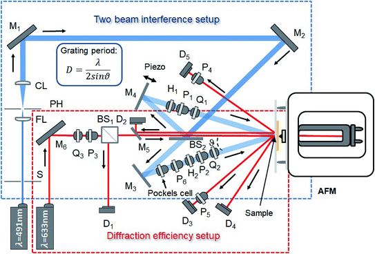
In order to study the surface relief grating (SRG) formation a novel set-up consisting of three parts is designed enabling in situ recording the change of the SRG-height and diffraction efficiency (DE) as a function of irradiation time (Fig. 1). The first part contains a two beam interference set-up that permits to generate well-defined spatiotemporal intensity or polarization interference patterns by changing polarization of two interfering beams in a controlled manner. In this part of the set-up the laser beam (λ = 491 nm) is spatially expanded and then collimated with a pair of focusing and collimating lenses and a pinhole (Fig. 1). Additionally, a 50![[thin space (1/6-em)]](https://www.rsc.org/images/entities/char_2009.gif) :
:![[thin space (1/6-em)]](https://www.rsc.org/images/entities/char_2009.gif) 50 beam splitter is added in order to separate the initially single beam into two beams of the same intensity. These two beams then pass through a set of wave plates and polarizers allowing independent control of intensity and polarization. For instance, adding a lambda quarter plate to each of the beam paths of the interference set-up, one with an angle of +45° and the second with an angle of −45° with respect to the optical axis, results in the right-left-circular interference pattern (RL). The second part of the home made set-up is an atomic force microscope (AFM) enabling measurements of the polymer topography changes in situ, i.e. even while irradiation conditions are varying. The sample is orientated with the polymer surface pointing towards the AFM tip, such that irradiation is “from below”, i.e., through the glass surface (Fig. 1).
50 beam splitter is added in order to separate the initially single beam into two beams of the same intensity. These two beams then pass through a set of wave plates and polarizers allowing independent control of intensity and polarization. For instance, adding a lambda quarter plate to each of the beam paths of the interference set-up, one with an angle of +45° and the second with an angle of −45° with respect to the optical axis, results in the right-left-circular interference pattern (RL). The second part of the home made set-up is an atomic force microscope (AFM) enabling measurements of the polymer topography changes in situ, i.e. even while irradiation conditions are varying. The sample is orientated with the polymer surface pointing towards the AFM tip, such that irradiation is “from below”, i.e., through the glass surface (Fig. 1).
To obtain at the same time information about the alignment of the azobenzene side chains in the polymer film, a red probe laser beam (HeNe, 633 nm) is integrated into the set-up. Its wave length of 633 nm falls out of the absorption bands of both polymers studied in this work and does not affect the polymer film, so that diffraction efficiency (DE) of the formed SRG can be recorded simultaneously. With our set-up we can acquire the intensity of the diffraction pattern in reflection mode in order to determine the DE of the first order diffraction (Fig. 1). To calibrate the DE, a beam splitter with the ratio of (T90/R10) is used in the DE set-up, such that 90% of the light arrives on the sample and 10% on a photodiode. The signal of this photodiode is recorded during the whole measurement for controlling the stability of the probe beam (and its intensity I0 prior to arrival at the sample) during the experiment. The diffraction efficiency is defined as the ratio of the intensity of diffraction order (IDO) and the intensity of the incoming light (I0):  , where I0 is 90% of the total intensity of the probe beam. The DE set-up additionally includes a lambda quarter wave plate converting the polarization of the probe beam from linear to circular. By adding a polarizer one can deliberately set the polarization state of the probe beam (e.g. S- or P-polarization). By adding a polarizer in front of the photodetector, one can measure both components of the diffracted light: polarized in plane (further denote as 1st order DE (P), measured by photodiode D3) and out of plane (cross-polarized, further denote as 1st order DE (S), measured by photodiode D5) with the probe beam. From the cross-polarized component one can directly obtain information about the birefringent grating, i.e. alignment of the azobenzene side chains within the polymer film. The set-up allows also to record the 2nd order DE (photodiode D4) and the directly reflected light (0th order of diffraction, photodiode D2). Adding a piezo actuator to the set up permits nanometer sized position control of mirror M4 (see Fig. 1) for shifting the interference pattern across the polymer film plane in a defined way. Repositioning the mirror simply introduces a phase delay between the two interfering beams, resulting in a change of the local distribution of the polarization vector within interference pattern. A Pockels cell and a polarizer are further placed in the second beam line acting as a fast optical switch. Applying the “lambda half” voltage periodically to the Pockels cell one can rotate the polarization of the writing beam by 90° such that the light either passes the polarizer or is blocked. In this way, we are able to switch rapidly between two-beam interference and the single beam “erase” configuration of the set-up. The three different set-ups: two beam interference, AFM and DE acquisition are controlled and operated with software specifically designed by us to record signals of the photodiodes, control the irradiation shutter, position the mirror and apply voltage on the Pockels cell. The computer generated signals regulate, with the help of an AD/DA converter, the irradiation, the voltage send to the piezo-controller and the high-voltage-amplifier used for driving the Pockels cell. These signals are recorded in the diffraction efficiency set-up as well as with the AFM by sending the signals to the aux-input of the AFM controller.
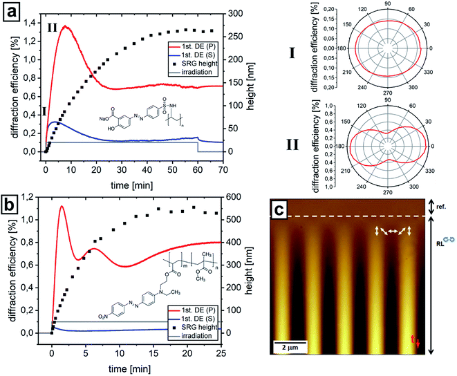
Fig. 2 shows the in situ recorded SRG height and DE signal for the Pazo and poly(MMA-co-DR1A) polymer films as a function of irradiation time. The probe beam is p-polarized for all results discussed in this paper, while one photodiode measures the intensity of the first order diffraction in-plane (1st order DE (P)), and the second one measures first order diffraction out-of-plane (1st order DE (S)). The presence of the out-of-plane component of the signal indicates that due to the interaction with the sample the polarization of the p-probe beam is rotated. In the case of the Pazo polymer, the DE signal of the first order diffraction on both photodiodes (red and blue curves in Fig. 2a) continuously increases during irradiation with a RL interference pattern (IP). The DE signals in-plane (red curve, 1st DE (P)) and out of plane (blue curve, 1st DE (S)) start to decrease when the SRG height reaches 120 nm and 60 nm, respectively. This behavior follows directly from the Raman–Nath theory56,57 and gives rise to describe intensity variation as a function of SRG height by Bessel function first kind of order. The ratio of the in-plane and out-of-plane component of the 1st order DE is changing with time. At the beginning (after 30 s of irradiation) the first order diffraction is circularly polarized (Fig. 2a(I)), while for longer irradiation times (more than 3 min) the in-plane component is dominating (Fig. 2a(II)). The polar plot in Fig. 2a(I and II) is measured by switching off the pump beam and recording the intensity of the first order diffraction as a function of rotation angle by rotating the polarizer in front of photodiode D3 (in plane component). After 1 hour irradiation the SRG height is 260 nm. The saturation in the SRG growth under irradiation with RL interference patterns for a 1 μm thick film is achieved after ca. 10 hours of irradiation at which the height is around 900 nm.
In the case of the second polymer studied here (poly(MMA-co-DR1A)), the saturation of the SRG height is already achieved after 15 minutes of irradiation with the final value of 550 nm (total film thickness of 600 nm). The DE is showing similar behavior as in the case of the Pazo polymer film, but due to the rapid evolution of the grating, the characteristic 1st order DE (P) peak is reached faster, i.e. after 86 seconds of irradiation, at which the SRG height is again 120 nm (Fig. 2b). There is also no significant out of plane component in the first order DE noticeable (see blue curve 1st DE (S) in Fig. 2b).
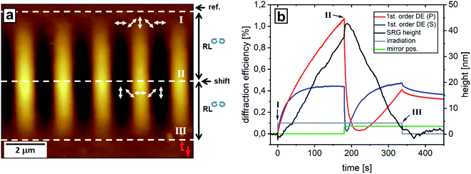
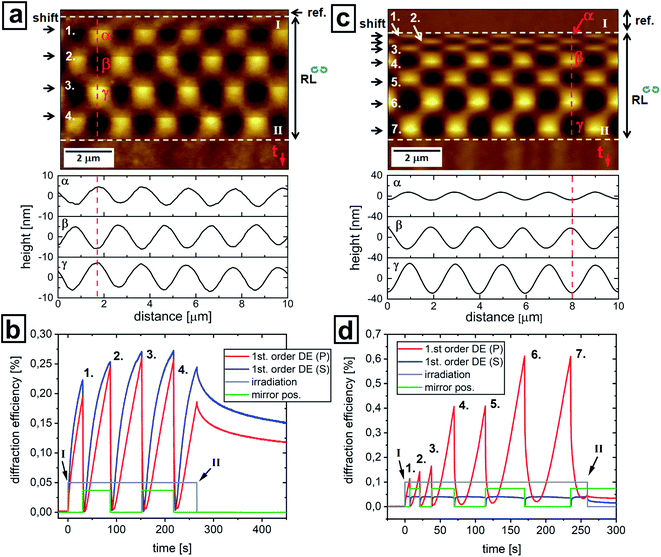
With the above described set-up we are able to generate a reversible switching of the polymer topography between a structured and a flat state utilizing irradiation with changing interference patterns. This was achieved by changing the position of the mirror M4 (see Fig. 1) during irradiation which results in a lateral shift of the whole interference pattern along the polymer topography. Fig. 3 shows the results of shifting the interference pattern by half of the optical period for Pazo polymer film. The experiment is performed as follows: first the sample is irradiated for 180 seconds with RL polarization IP (onset of irradiation is shown by 1st dashed white line at the top of Fig. 3a). Polarization IP means that the intensity along the sample is constant, while the orientation of the electric field vector (see white arrows in Fig. 2c and 3a) varies locally with a certain period (optical period, Λ). This first irradiation step generates a grating height of 40 nm (Fig. 3a). Afterwards the local distribution of the electrical field vector is shifted by half of the optical period, which corresponds to 90° rotation of local electrical field vector (see white arrows in Fig. 3a). After the shift the SRG height continuously decreases till a flat topography is reached (dashed white line at the bottom of Fig. 3a). At this point the irradiation is stopped. This erase process is slightly faster (160 s, i.e. 0.29 nm s−1 of topography flattening) compared to SRG inscription (180 s, 0.20 nm s−1 of topography increase). A possible explanation is that the initial state of both processes is different. During irradiation with IP and corresponding cyclic trans–cis photoisomerization the azobenzene groups rotate to align perpendicularly with their main axis to the electrical field vector resulting in locally ordered domains. Since in the case of the SRG formation the azobenzene molecules are initially randomly orientated within the polymer film, the time needed for local azobenzene alignment is larger than in the case of irradiation with shifted interference patterns. In this case, due to local rotation of the electric field vector by 90°, the probability to absorb light by the aligned azobenzene molecules is larger thus resulting in a faster kinetics of topography response. At the point where the interference pattern is shifted, a fast jump in the SRG height of 5 nm became noticeable followed by a linear decrease (Fig. 3b, black curve). The explanation for this behavior is based again on local pre-orientation of the azobenzene molecules during the first step of irradiation. At the point of IP shifting all the aligned molecules are able to absorb incoming light resulting in noticeable increase of the free volume in polymer film and as a consequence its height increases.
The in-plane component of the diffraction efficiency of the first order diffraction (red curve, 1st order DE (P), in Fig. 3b) continuously increases with SRG height. The out of plane component (blue curve, 1st order DE (S), in Fig. 3b) saturates after a certain time. At the point where the interference pattern is shifted, there is fast drop (within 6 seconds) of out-of-plane component (blue curve in Fig. 3b), at this point the SRG height and the out-of-plane component contribute to the overall DE signal. After 37 seconds the in-plane component (red curve in Fig. 3b) settles to zero, while the increasing 1st order DE (S) component and the left SRG result in DE signal of 0.4%.
A short time after shifting of the IP, both components of the DE, i.e. in- and out-of-plane, start to increase, while the SRG height decreases. At the point where the topography becomes flat there is nevertheless still significant DE signal indicating the formation of a new birefringent grating from alignment of azobenzene groups in the bulk. In this case the erase process with shifting the interference pattern can be understood as erasing the primary, topographical SRG and forming a new birefringent grating in the bulk. Further irradiation will create a new SRG but shifted by half an optical period as described below (see Fig. 5).
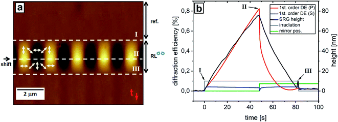
A similar behavior is also observed in case of poly(MMA-co-DR1A) polymer films (Fig. 4). Since the response of this polymer on irradiation is faster, the first exposure to RL IP lasts for only 48 seconds resulting in a grating height of 80 nm (speed of grating increase is 1.7 nm s−1). After shifting the interference pattern by half a period, the topography is flattened within only 34 seconds (speed of grating decrease is 2.1 nm s−1) (Fig. 4). At the point where the topography is flat again, there is a small signal in the 1st order DE indicating the formation of new bulk phase grating. The out-of-plane component in the DE (blue curve, 1st order DE (S), in Fig. 4b) is negligible. In contrast to the Pazo polymer film there is no jump in the SRG height detected at the point where the interference pattern is shifted. One possible explanation for this is that due to the fast response on irradiation, the topography jump is completed within a time too short for the AFM to detect it.
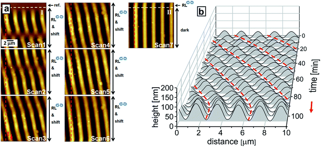
In the previous experiments the irradiation is stopped when the surface is flattened, but in case of further irradiation after IP shifting, the formation of a new SRG is observed with positions of maxima and minima interchanged (Fig. 5). Moreover, when the IP is shifted back to its initial distribution, the primary SRG is recovered. This procedure can be conducted repeatedly, as shown in Fig. 5, where the continuous scan with repeated shifts leads to a checkerboard pattern in the AFM recording. For the Pazo polymer, the irradiation is stopped after 4 cycles of IP shifting, at a point where the surface has just been rendered flat again (Fig. 5a).
The presence of the diffraction efficiency signal (red and blue curves in Fig. 5b) indicates the existence of bulk birefringent grating due to local alignment of the azobenzene side groups. This phase grating decreases in the dark indicating orientation relaxation of the azobenzenes with time. A similar experiment is performed in the case of poly(MMA-co-DR1A) polymer films that permits the same reversible surface structuring (Fig. 5c and d). In this case, the shifting is carried out seven times as indicated in Fig. 5c. Here, the irradiation time for each step is increased between successive shifting events resulting in a continuous increase in SRG height showing also here the independency of the erase process from the SRG height. By continuously shifting the interference pattern, e.g. by applying a saw-tooth signal to the piezo, one can shift the SRG over several micrometers (Fig. 6).
In this way, we are able to induce fluctuations in the polymer topography resembling propagation of the water wave (Fig. 6b). To achieve continuous change in the polymer topography without intermittent flat state, we shift the IP in each subsequent step by fourth of the optical period which results in propagation of the primary topography maxima/minima over 14 μm to the right (see Fig. 6b). The corresponding changes in the DE signal are shown in Fig. S2 (see ESI†).
Summarizing this part we can state that the erasure of the polymer topography by applying shifts to the interference patterns (i.e. rotating the local distribution of the electric field vector by 90°) is an efficient and fast process which proceeds by overwriting the initial SRG by a new bulk birefringent grating. In order to estimate the efficiency of this erase mechanism, we compare in the following how erasure can be achieved alternatively by applying a single beam or by thermal treatment.
Erasing a SRG pattern with a single laser beam
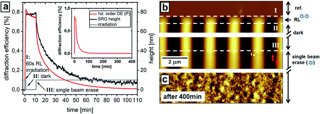
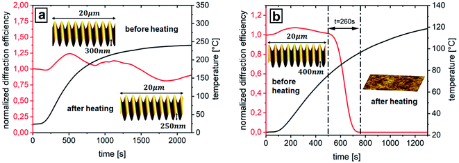
A fast optical switch is integrated into the set-up in order to turn off one of the two interfering beams. This is achieved by employing a Pockels cell and an additional polarizer (see Fig. 1). By applying the lambda-half voltage on the Pockels cell the polarization of the writing beam is rotated by 90° so that the light will be blocked by the subsequent polarizer. This established a very fast switching between two-beam and single beam erasure. Due to the two integrated lambda quarter plates of the RL interference pattern, the single beam is also circularly polarized, which can be expected to induce an effective erasure process.48 Fig. 7 shows the results of the single beam experiment performed with a poly(MMA-co-DR1A) structured polymer film. The film was first irradiated with RL IP for 1 minute resulting in 80 nm SRG height. Afterwards the writing beam is switched off for 10 minutes. During this time the in-plane component of the 1st order DE drops exponentially while the SRG height stays constant (Fig. 7). In the following step switching on the erase beam results in fast decrease of the DE signal and SRG height. The irradiation is stopped after 400 min when no diffraction efficiency signal could be detected. At this point the polymer film is found to be atomically smooth (see Fig. 7c). In the case of Pazo polymer the erasure with the circularly polarized beam does not result in a complete flattening of the polymer topography as well as vanishing of DE signal even after 20 h of irradiation (see ESI, Fig. S1†). Comparing these results with those obtained by the shifting procedure (Fig. 3 and 4) shows that erasure via shifting is indeed much faster for both polymers, but the final state of the flattened polymer film is different. In the case of single beam erasure, the alignment of azobenzene molecules introduced by the IP irradiation is getting destroyed and transformed to a random orientation indicated by decreasing of DE signal. Shifting the interference pattern eliminates the grating topography by overwriting the initial birefringent grating with a new one. At the point of a flat surface the bulk is already reoriented with a pure phase grating which can directly be seen in the DE (red and blue curves in Fig. 3b).To compare the optically induced SRG erasure process to the thermal one, we employed another home-made set-up consisting of a hot plate with a temperature sensor onto which the sample is placed, and an optical part facilitating red laser beam for measurements of diffraction efficiency to be directed at the polymer sample. As can be seen from Fig. 8 the erasure of a 400 nm high grating of poly(MMA-co-DR1A) sets in at ca. 80 °C (Tg ∼ 102 °C)58 and after ca. 260 seconds the diffraction efficiency signal drops to zero (Fig. 8b). So, the thermal erasure needs around 5 minutes and heating up to 100 °C, while optical erasure by IP shifting takes place within 34 seconds at room temperature. Single beam erasure requires the most time (400 min). In contrast, it was not possible to flatten Pazo film thermally. Indeed, heating up to 250 °C, at which the decomposition of the polymer materials sets in (see TGA measurement in ESI, Fig. S3a†), does not result in decrease of the diffraction efficiency signal (red curve in Fig. 8a), the SRG height is also only slightly affected: it drops from 300 to 250 nm within 30 minutes of heating at 250 °C. As can be seen from DSC measurements (ESI, Fig. S3b†), there is no clear indication of the glass transition temperature. This result is in contrast to the work published by Ferreira et al., who measured 95 °C as Tg for this polymer,59 but in a good agreement with the results of Stumpe et al.60 where it was reported that the SRG inscribed in Pazo could not be erased by heating at 200° over 6 hours. This is explained by the presence of ionic interactions in the side chains of the Pazo (see chemical structure in Fig. 2a).61,62 Thus with these results, we can state that the erasure of the surface relief grating of Pazo polymer can be done quite easily and fast (160 seconds of irradiation at room temperature) using the IP shifting method (Fig. 3), with single beam the procedure takes 20 hours and does not result in complete elimination of the grating, while the thermal erasure is not possible at all. These experiments show that the temperature stability of the SRG depends on the polymer structure itself.
Conclusions
Here we have reported on the reversible surface structuring of photosensitive polymer films using a novel method of fast SRG erasure simply by shifting the interference pattern by half an optical period. This is achieved by utilizing a home-made set-up to record the changes in the surface relief grating (SRG) and the diffraction efficiency (DE) signal upon irradiation with varying interference patterns in situ. Our setup also permits to separate the SRG part from the birefringent grating component in the DE, so that we can directly probe the molecular orientation of the azobenzene moieties in the bulk. Integrating a phase delay stage into the two beam interference set-up allows for shifting the interference patterns along the sample plane; in this way the polymer surface can be rendered “dynamic”. A shift of half of the optical period leads to erasure of the just created surface grating by inscribing a new birefringent grating in the bulk. Depending on the polymer material this leads to the generation of a pure phase grating without any surface structure (with the interesting example of the Pazo polymer studied here). The reversibility of the surface structuring is demonstrated for two different polymers. Attempts to erase the SRG by single beam irradiation and a change in the temperature required significantly more effort than optical shifting method. In the case of thermal erasure, the Pazo polymer is found to be stable such that both gratings, topographical and the bulk birefringence withstand temperatures up to 250 °C over hours of heating, while in the poly(MMA-co-DR1A) film the SRG is erased completely with heating at the glass transition temperature Tg during 5 minutes. Erasing SRGs with a single circularly polarized beam is feasible, but requires 400 minutes of irradiation time for poly(MMA-co-DR1A), while the more rigid polymer Pazo takes more than 20 hours of irradiation. In contrast, the optical shift method reduces these times to only 160 seconds and 34 seconds irradiation time for Pazo and poly(MMA-co-DR1A) polymers, respectively. This phenomenon is simply related to the fact that shifting the interference pattern produces a pure phase grating with a flat topography, while erasing with a single beam completely destroy the grating restoring the initial amorphous state of the polymer film and thus requires more time. The method proposed here bears one decisive advantage: patterns in topography and other optical properties such as birefringence are inscribed at the same time. By using the peculiar dynamics and depending on the protocol of optical settings we can end up with topographical and optical (birefringence) patterns, or combinations thereof. This might lead to hitherto unprecedented applications as indicated in the introduction.Conflicts of interest
There are no conflicts to declare.Acknowledgements
This research is supported by the Helmholtz Graduate School on Macromolecular Bioscience (Teltow, Germany) and German-Russian Interdisciplinary Science Center (G-RISC). We thank Prof. Dr Carsten Henkel and Burkhard Stiller for the fruitful discussions. We thank Prof. I. Zvereva (Centre of Thermal Analysis and Calorimetry, St. Petersburg State University) for the support in measurements and interpretation of TGA and DSC results.References
- D. Liu and D. J. Broer, Responsive Polymer Surfaces: Dynamics in Surface Topography, Wiley-VCH, Weinheim, Germany 2017 Search PubMed.
- L. Dong, A. K. Agarwal, D. J. Beebe and H. Jiang, Nature, 2006, 442, 551 CrossRef CAS PubMed.
- T. M. de Jong, D. K. G. de Boer and C. W. M. Bastiaansen, Opt. Express, 2011, 19, 15127–15142 CrossRef PubMed.
- M. Yamada, M. Kondo, J. Mamiya, Y. Yu, M. Kinoshita, C. J. Barrett and T. Ikeda, Angew. Chem., Int. Ed. Engl., 2008, 47, 4986 CrossRef CAS PubMed.
- S. Hvilsted, C. Sanchez and R. Alcala, J. Mater. Chem., 2009, 19, 6641–6648 RSC.
- M. Ibn-Elhaj and M. Schadt, Nature, 2001, 410, 796 CrossRef CAS PubMed.
- T. S. Wong, S. H. Kang, S. K. Y. Tang, E. J. Smythe, B. D. Hatton, A. Grinthal and J. Aizenberg, Nature, 2011, 477, 443 CrossRef CAS PubMed.
- L. M. Goldenberg, V. Lisinetskii, Y. Gritsai, J. Stumpe and S. Schrader, Laser Phys. Lett., 2013, 10, 085804 CrossRef.
- L. M. Goldenberg, V. Lisinetskii, Y. Gritsai, J. Stumpe and S. Schrader, Adv. Mater., 2012, 24, 3339 CrossRef CAS PubMed.
- T. Alasaarela, D. Zheng, L. Huang, A. Priimagi, B. Bai, A. Tervonen, S. Honkanen, M. Kuittinen and J. Turunen, Opt. Lett., 2011, 36, 2411–2413 CrossRef PubMed.
- R. H. Bishop, in Mechatronics: An Introduction, ed. T. Francis, Taylor and Francis Group, Oxfordshire, England, 2006, p. 312 Search PubMed.
- S. Loebner, J. Jelken, N. S. Yadavalli, E. Sava, N. Hurduc and S. Santer, Molecules, 2016, 21, 1663 CrossRef CAS PubMed.
- S. L. Oscurato, F. Borbone, P. Maddalena and A. Ambrosio, ACS Appl. Mater. Interfaces, 2017, 9, 30133–30142 CrossRef CAS PubMed.
- N. A. Malvadkar, M. J. Hancock, K. Sekeroglu, W. J. Dressick and M. C. Demirel, Nat. Mater., 2010, 9, 1023 CrossRef CAS PubMed.
- P. Zhang, H. Liu, J. Meng, G. Yang, X. Liu, S. Wang and L. Jiang, Adv. Mater., 2014, 26, 3131–3135 CrossRef CAS.
- X. Qiu, J. Appl. Phys., 2010, 108, 011101 CrossRef.
- D. Liu, N. B. Tito and D. J. Broer, Nat. Commun., 2017, 8, 1526 CrossRef PubMed.
- W. Feng, D. J. Broer and D. Liu, Adv. Mater., 2018, 30, 1704970 CrossRef PubMed.
- A. H. Gelebart, D. J. Mulder, M. Varga, A. Konya, G. Vantomme, E. W. Meijer, R. L. B. Selinger and D. J. Broer, Nature, 2017, 546, 632–636 CrossRef CAS PubMed.
- K. Kumar, A. P. H. J. Schenning, D. J. Broer and D. Liu, Soft Matter, 2016, 12, 3196–3201 RSC.
- A. J. J. Kragt, D. J. Broer and A. P. H. J. Schenning, Adv. Funct. Mater., 2018, 28, 1704756 CrossRef.
- D. Liu, L. Liu, P. R. Onck and D. J. Broer, Proc. Natl. Acad. Sci. U. S. A., 2015, 112, 3880–3885 CrossRef CAS PubMed.
- A. Kopyshev, C. J. Galvin, R. R. Patil, J. Genzer, N. Lomadze, D. Feldmann, J. Zakrevski and S. Santer, ACS Appl. Mater. Interfaces, 2016, 8, 19175 CrossRef CAS PubMed.
- P. Rochon, E. Batalla and A. Natansohn, Appl. Phys. Lett., 1995, 66, 136–138 CrossRef CAS.
- D. Y. Kim, S. K. Tripathy, L. Li and J. Kumar, Appl. Phys. Lett., 1995, 66, 1166–1168 CrossRef CAS.
- C. J. Barrett, P. Rochon and A. Natansohn, J. Chem. Phys., 1998, 109, 1505–1516 CrossRef CAS.
- K. G. Yager and C. J. Barrett, Curr. Opin. Solid State Mater. Sci., 2001, 5, 487–494 CrossRef CAS.
- T. König, N. S. Yadavalli and S. Santer, J. Mater. Chem., 2012, 22, 5945–5950 RSC.
- T. König, V. V. Tsukruk and S. Santer, ACS Appl. Mater. Interfaces, 2013, 5, 6009–6016 CrossRef PubMed.
- Th. Papke, N. S. Yadavalli, C. Henkel and S. Santer, ACS Appl. Mater. Interfaces, 2014, 6, 14174–14180 CrossRef CAS PubMed.
- A. Kopyshev, C. J. Galvin, J. Genzer, N. Lomadze and S. Santer, Polymer, 2016, 98, 421–428 CrossRef CAS.
- A. Kopyshev, N. Lomadze, D. Feldmann, J. Genzer and S. Santer, Polymer, 2015, 79, 65–72 CrossRef CAS.
- J. Vapaavuori, A. Goulet-Hanssens, I. T. S. Heikkinen, C. J. Barrett and A. Priimagi, Chem. Mater., 2014, 26, 5089–5096 CrossRef CAS.
- J. E. Koskela, J. Vapaavuori, R. H. A. Ras and A. Priimagi, ACS Macro Lett., 2014, 3, 1196–1200 CrossRef CAS.
- N. S. Yadavalli, T. König and S. Santer, J. Soc. Inf. Disp., 2015, 23, 154–162 CrossRef CAS.
- T. König, L. M. Goldenberg, O. Kulikovska, L. Kulikovsky, J. Stumpe and S. Santer, Soft Matter, 2011, 7, 4174–4178 RSC.
- V. Toshchevikov, J. Ilnytskyi and M. Saphiannikova, J. Phys. Chem. Lett., 2017, 8, 1094–1098 CrossRef CAS PubMed.
- N. S. Yadavalli, D. Korolkov, J. Moulin, M. Krutyeva and S. Santer, ACS Appl. Mater. Interfaces, 2014, 6, 11333–11340 CrossRef CAS PubMed.
- N. S. Yadavalli, F. Linde, A. Kopyshev and S. Santer, ACS Appl. Mater. Interfaces, 2013, 5, 7743–7747 CrossRef CAS PubMed.
- G. Di Florio, E. Bründermann, N. S. Yadavalli, S. Santer and M. Havenith, Nano Lett., 2014, 14, 5754–5760 CrossRef CAS PubMed.
- J. Ilnytskyi and M. Saphiannikova, ChemPhysChem, 2015, 16, 3180–3189 CrossRef CAS PubMed.
- J. M. Ilnytskyi, D. Neher and M. Saphiannikova, J. Chem. Phys., 2011, 135, 044901 CrossRef PubMed.
- V. Toshchevikov, M. Saphiannikova and G. Heinrich, J. Phys. Chem. B, 2012, 116, 913–924 CrossRef CAS PubMed.
- V. Toshchevikov and M. Saphiannikova, J. Phys. Chem. B, 2014, 118, 12297–12309 CrossRef CAS PubMed.
- V. Toshchevikov, M. Saphiannikova and G. Heinrich, J. Phys. Chem. B, 2009, 113, 5032–5045 CrossRef CAS PubMed.
- K. G. Yager and C. J. Barrett, J. Chem. Phys., 2007, 126, 094908 CrossRef PubMed.
- T. M. Geue, M. G. Saphiannikova, O. Henneberg, U. Pietsch, P. L. Rochon and A. L. Natansohn, Phys. Rev. E: Stat., Nonlinear, Soft Matter Phys., 2002, 65, 052801 CrossRef CAS PubMed.
- J. Vapaavuori, R. H. A. Ras, M. Kaivola, C. G. Bazuin and A. Priimagi, J. Mater. Chem. C, 2015, 3, 11011–11016 RSC.
- A. Tofini, L. Levesque, O. Lebel and R. G. Sabat, J. Mater. Chem. C, 2018, 6, 1083–1091 RSC.
- F. L. Labarthet, T. Buffeteau and C. Sourisseau, J. Phys. Chem. B, 1998, 102, 2654–2662 CrossRef CAS.
- F. L. Labarthet, P. Rochon and A. Natansohn, Appl. Phys. Lett., 1999, 75, 1377–1379 CrossRef.
- F. L. Labarthet, J. L. Bruneel, T. Buffeteau and C. Sourisseau, J. Phys. Chem. B, 2004, 108, 6949–6960 CrossRef CAS.
- N. S. Yadavalli and S. Santer, J. Appl. Phys., 2013, 113, 224304 CrossRef.
- N. S. Yadavalli, M. Saphiannikova, N. Lomadze, L. M. Goldenberg and S. Santer, Appl. Phys. A, 2013, 113, 263–272 CrossRef CAS.
- N. S. Yadavalli, M. Saphiannikova and S. Santer, Appl. Phys. Lett., 2014, 105, 051601 CrossRef.
- A. Emoto, S. B. Baharim, T. Sasaki, T. Shioda, A. Ogiwara and H. Ono, Jpn. J. Appl. Phys., 2010, 49, 122502 CrossRef.
- C. V. Raman and N. S. Nagendra Nathe, Proc. Indian Acad. Sci. Sect. A, 1935, 2, 406–412 CrossRef.
- As provided by Sigma Aldrich.
- Q. Ferreira, P. A. Ribeiro, O. N. Oliveira and M. Raposo, ACS Appl. Mater. Interfaces, 2012, 4, 1470–1477 CrossRef CAS PubMed.
- L. M. Goldenberg, O. Kulikovska and J. Stumpe, Langmuir, 2005, 21, 4794 CrossRef CAS PubMed.
- Q. Zhang, X. Wang, C. J. Barrett and C. G. Bazuin, Chem. Mater., 2009, 21, 3216 CrossRef CAS.
- J. Vapaavuori, C. G. Bazuin and A. Priimagi, J. Mater. Chem. C, 2018, 6, 2168 RSC.
Footnote |
| † Electronic supplementary information (ESI) available. See DOI: 10.1039/c9ra02571e |
| This journal is © The Royal Society of Chemistry 2019 |

