 Open Access Article
The direct-writing of low cost paper based flexible electrodes and touch pad devices using silver nano-ink and ZnO nanoparticles†
Kamlesh Shrivas *ab,
Archana Ghosalea,
Tushar Kantb,
P. K. Bajpaic and
Ravi Shankard
aDepartment of Chemistry, Guru Ghasidas Vishwavidyalaya, Koni, Bilaspur, CG, India. E-mail: kshrivas@gmail.com
bSchool of Studies in Chemistry, Pt. Ravishankar Shukla University, Raipur, 492010, CG, India
cDepartment of Pure and Applied Physics, Guru Ghasidas Vishwavidyalaya, Koni, Bilaspur, CG, India
dNanoscience and Nanoengineering Program, South Dakota School of Mines and Technology, Rapid City, South Dakota 57701, USA
First published on 6th June 2019
Abstract
We report a novel and simple approach for the synthesis of silver nanoparticles capped with inositol (Ag NPs/Ino) by the reduction of silver salt with ascorbic acid under basic conditions. UV-vis, TEM, FTIR and TGA techniques were used to characterize the Ag NPs/Ino to determine the size, shape and surface modification of the NPs. Stable silver nano-ink was prepared in aqueous solution containing 1% PVP (stabilizer) and glycerol (cosolvent) and was used for the direct-writing of a paper electrode with a roller ball-point pen for electrochemical applications. The solvent, stabilizing agents, concentration of NPs (10%), paper substrate, sintering temperature (40 °C) and sintering time (15 min) were optimized to obtain a uniform coating of Ag NPs on the paper substrate. Further, the synthesis and fabrication of ZnO NPs on a paper substrate was put forward to design a touch pad device based on the piezoelectric effect. The preparation of paper based devices suggests a direction for the development of a simple, low cost and compatible approach for the direct-writing of paper based flexible electrodes and electronics for future applications.
Introduction
The preparation of functional conductive materials has been widely investigated by several researchers for a variety of applications such as transistors,1 displays,2 solar cells,3 capacitors,4 and touch pads.5 Among these, the touch pad is basically made of an input device for sending the signals to an appliance by mechanical touch with a finger. It acts as an interface between the finger of a person and the device. The main phenomenon involved in this process is the piezoelectric effect where the pressure applied on the solid surface will transform the electric current to the device for a desired function.6 Commonly, substrates used are made of polymeric and plastic materials for preparation of flexible touch pad devices.7 The disadvantages of using these type of substrate are they are expensive and non-biodegradable. Recently, paper has been used as a substrate for preparation of flexible electronics because it is commercially and easily available with different sizes, width and porosity. It provides the fabrication of functional materials for the preparation of low cost, biodegradable and flexible electronics.8 Paper is composed of a natural polymer of cellulose with multiple folding and compact 3D structures with pores. Hence, a paper based touch pad is prepared where the flow of piezoelectricity is due to the fabrication of functional nanomaterials on the paper substrate.9The term piezoelectricity is referred to the electricity produced as result of a change in pressure and latent heat. It is derived from the Greek word ‘piezein’, which means ‘to press’ or ‘to squeeze’. Therefore, piezoelectricity is a flow of electric charge that mounts on certain solid materials due to the applied mechanical stress. Piezoelectricity is a result of linear electromechanical interaction between mechanical and electrical states on crystalline materials with no inversion of symmetry and it is a reversible process.10 There are various materials that show piezoelectric properties such as certain crystals, ceramics and also some biomolecules (e.g. DNA and certain proteins). Nanoparticles (NPs), such as ZnO,11,12 ZnS,13 CdS14 and CdSe15 also show piezoelectric properties. Among these, ZnO NPs exhibited extraordinary semiconducting and piezoelectric properties with good stability and cost effectiveness. Thus, they are a better choice for the preparation of piezoelectric devices from this type of nanomaterial.
The connectivity of piezoelectric devices is created through plastic wires which are found to be complex and expensive. This can be minimized by the preparation of a fabricated conductive electronic circuit with metal NPs. The fabricated circuit can be made from conductive NPs such as (Au),16 silver (Ag)17 and copper (Cu).18 Among these, Ag NPs showed a better conductive property and comparatively low cost compared to gold NPs. Thermal methods such as microwave irradiation19,20 and chemical reduction21 are reported for the preparation of Ag NPs. The wet chemical method is commonly used for preparation of Ag NPs by the reduction of metal salts of silver with sodium borohydride, hydrazine or ascorbic acid as the reducing agent. Dispersions and suspensions of NPs have attracted interest due to their large variety of applications in various fields such as chemistry, biology, medical and material sciences.22–24 The preparation of homogenous dispersed and stable NPs is very important because of its simplicity in fabricating a conductive track on a paper substrate. Stable and homogenous dispersed NPs in solvent would require the NPs to be covered with certain stabilizing molecules which prevent them from aggregation. Thus, the NPs are stabilized with certain polymers (PVA, PVP and chitosan) in solvent which kept the particles stabilized for long periods of time. If the coating material does not form stable clusters then stabilizers are added in very small amounts to form a homogenous stable phase.25–27 The methods for fabrication of conductive NPs on a solid surface are done through printing, lithography, stamping, chemical vapor deposition, sputtering, spin coating and direct-writing. The method of direct-writing is easy, user friendly and cost effective. It does not require any expensive and tedious equipment for the fabrication of functional materials on substrate materials.28,29
In this work, Ag NPs capped with inositol (Ag NPs/Ino) were synthesized by the reduction of silver salt with ascorbic acid in basic conditions where inositol was used as the capping agent. The solvent, stabilizing agents (PVP, PVA and chitosan) and concentration of NPs were optimized for the preparation of stable ink; the sintering temperature and sintering time were optimized for obtaining a uniform coating of NPs on different paper substrates. The fabricated NPs on the photo paper substrate were tested as a working electrode in cyclic voltammetry for electrochemical applications. In addition, the novel piezoelectric touchpad was prepared by deposition of ZnO NPs on the conductive track of Ag NPs. The produced piezoelectric current after applying mechanical stress by pressing on the paper substrate through the finger tip was measured using amperometry.
Experimental section
Reagents
Silver nitrate, ascorbic acid, acetone, methanol, potassium chloride, polyvinyl alcohol (PVA), polyvinylpyrrolidone (PVP), inositol (Ino), ammonia and chitosan were obtained from Himedia (Mumbai, India). Phosphate buffer solutions (PBS) of pH 7.0 prepared from NaH2PO4 and Na2HPO4 were obtained from Merck (Germany). All other chemicals and reagents used in this study were of analytical grade. Digital photo paper was purchased from the local stationary shop.Synthesis of Ag NPs/Ino
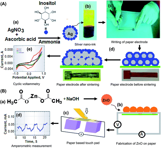
Ag NPs/Ino were synthesized by employing silver nitrate as a precursor and inositol as a capping agent in basic media as reported in the literature with slight modifications.29 The steps for the synthesis of Ag NPs capped with inositol are shown in Fig. 1A(a). Briefly, 300 mg of silver nitrate was dissolved in 10 mL of deionized water (DW) followed by the dropwise addition of ammonia solution until the color of the solution become transparent. Then, 150 mg of inositol was added into the solution mixture followed by the addition of 1 mL of 10% ascorbic acid solution. The solution mixture was stirred for 30 min at room temperature. The conversion of silver salt to Ag NPs was monitored by color change over different reaction periods, which was observed to change from colorless to grayish. After the completion of the reaction, the mixture was precipitated with methanol 3 times to remove the residual of the products. The grayish product of Ag NPs/Ino obtained was used for preparation of nano-ink.Preparation of silver nano-ink
A suitable amount of Ag NPs/Ino was dispersed in different solvents such as DW, methanol, ethylene glycol and iso-propanol.30,31 The prepared dispersed Ag NPs/Ino were tested for their dispersity and stability to use as a nano-ink. The homogenized nano-ink was obtained when DW was used as a solvent. However, the solution mixture was stable just for few hours. Therefore, very small amounts of stabilizers (PVP, PVA and chitosan) were added to each solution for their stabilities. In this way, three different types of inks with different stabilizing agents were prepared. Finally 10 μL of glycerol was added to the solution to provide sufficient moisture to the nano-ink solutions for stability. The prepared silver nano-ink is shown in Fig. 1A(b).Fabrication of the paper electrode with silver nano-ink using a roller-ball point pen
The prepared nano-ink was filled into the roller-ball point pen which was already cleaned with methanol and acetone several times. A 10 × 0.5 cm length with a base of 1 × 1 cm2 area was drawn on photo paper with a pen containing nano-ink. The sintering time and sintering temperature were optimized for better conductive responses of the prepared paper electrode and used for electrochemical applications.32 The fabrication of an electrode with direct-writing (Fig. 1A(c)), sintering (Fig. 1A(d)) and the application for measurement of electrochemical responses are shown in Fig. 1A(e).Synthesis of ZnO NPs
ZnO NPs were prepared by a hydrothermal method, a 10 mL zinc acetate (5 mM) solution was added dropwise into a 10 mL stirred solution of NaOH (5 mM).33 The appearance of a white precipitate in the solution showed the formation of ZnO NPs. The synthesis of ZnO NPs was performed for different reaction times from 15 to 60 min. The NPs were allowed to settle down and the solution was decanted and washed with methanol. The precipitate obtained was dried and used for fabricating the paper substrate to investigate the piezoelectric effect. The synthesis of ZnO NPs is shown in Fig. 1B(a).Fabrication of ZnO NPs on a paper substrate and connection with a silver conductive track
The ZnO NPs were dispersed in methanol using an ultrasonic bath for 5 min and then deposited onto the surface of paper (dimension 5 cm × 5 cm). This process was repeated 10 times to obtain better growth of ZnO NPs on the paper substrate. The surface of the paper is rich with hydroxyl (OH) groups which form a hydrogen bond with ZnO NPs. Thus, the growth of NPs onto the surface of paper was found to be stable for a long period of time with multiple mechanical stresses applied on the substrate.8For the piezoelectric study, a grown paper electrode with ZnO NPs was kept over two pillars and the whole system was fixed with an insulating adhesive sheet by keeping the ends of the electrode left open for connection with the potentiostat. The mechanical press was applied on the paper touch pad and the change in current was measured using amperometry. Fig. 1B(b) shows the fabrication of ZnO NPs on the paper substrate and Fig. 1B(c) shows the connection with the silver conductive track followed by the measurement of current with amperometry, which is shown in Fig. 1B(d).
Apparatus
A UV-visible spectrophotometer type-1800 (Shimadzu, Japan) matched with a 1 cm quartz cell was used for measurement of the localized surface plasmon resonance (LSPR) absorption band of Ag NPs/Ino. The shape and size of Ag NPs/Ino were determined by transmission electron microscopy (TEM). The surface modification of the Ag NPs with PVA was verified with Fourier transform-infrared (FTIR) spectroscopy, type-IRA affinity (Shimadzu, Japan). CV measurements and amperometric studies were performed using a PGSTAT 101 potentiostat operated by NOVA 1.10 software packages (Metrohm Autolab, Netherland). TGA was carried out in the temperature range from 0 to 900 °C with a rise of temperature at the rate of 10 °C min−1. Thermal gravimetric analysis (TGA) was done with a PerkinElmer STA 6000 simultaneous thermal analyzer with a scan rate of 10° min−1. The size distribution of the Ag NPs and ZnO NPs was estimated by the dynamic light scattering (DLS) measurements using the Nano-Zetasizer instrument (Malvern, UK).Results and discussion
Characterization of Ag NPs/Ino and ZnO NPs
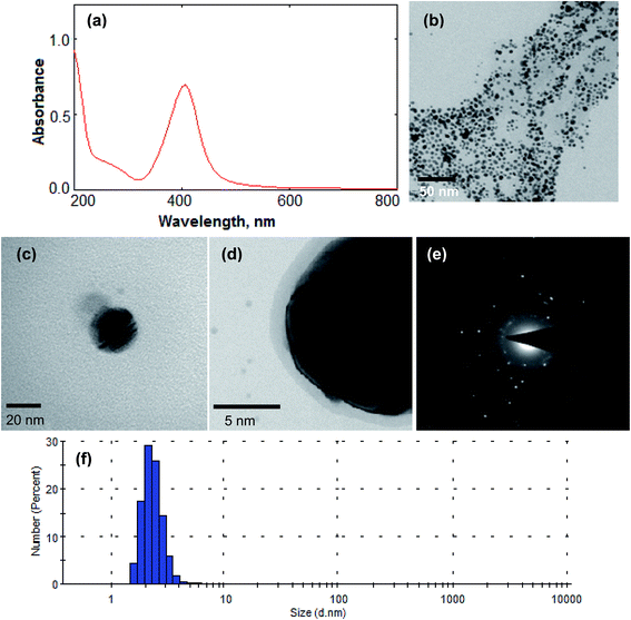
The size and shape of Ag NPs/Ino were established by measuring the LSPR absorption band of Ag NPs. The LSPR absorption band at visible region around 400–420 nm provided the size of NPs in the range of 10–60 nm.34 In the present study, the LSPR absorption band for Ag NPs/Ino was around 410 nm as shown in Fig. 2(a). TEM was used to determine the size of Ag NPs/Ino and the average size of the NPs was found to be 12.5 ± 1.6 nm (as shown in Fig. 2(b)). The enlarged view of Ag NPs/Ino shows the stabilization of the capping agent on the surface of the NPs in Fig. 2(c) and (d). Fig. 2(e) shows the selected area electron diffraction (SAED) pattern of silver NPs with fringes and bright circular rings corresponding to the (111), (200), (220) and (311) planes of silver showing that these NPs are highly crystalline in nature.35 The DLS measurement also confirmed the average size of the Ag NPs/Ino was about the same as the results obtained with TEM (shown in Fig. 2(f)).Moreover, for comparison of the IR data of Ag NPs/Ino before and after sintering at 40 °C was performed with Fourier transform-infrared (FTIR) as shown in Fig. 3(a). Moreover, the decrease in the peak intensity showed the removal of inositol from the surface of the Ag NPs after the sintering process. The peaks obtained in the range of 2920–2850 cm−1 are attributed to the CH2 symmetric and asymmetric stretching of the stabilizing molecule. The decrease in the signal intensity and slight shift of the peak bands verified the surface modification of the Ag NPs with inositol and the decline in concentration of inositol from the surface NPs.36 TGA analysis of Ag NPs/Ino was also done to study the thermal stability of NPs. In this process, 10 mg of Ag NPs/Ino was used to investigate the loss of the capping group from its surface against different temperatures. The result is shown in Fig. 3(b). The TGA curve showed the 92.0% weight loss of Ag NPs/Ino. The weight loss during the heating was due to degradation and evaporation of the capping molecules from the surface of the Ag NPs.37
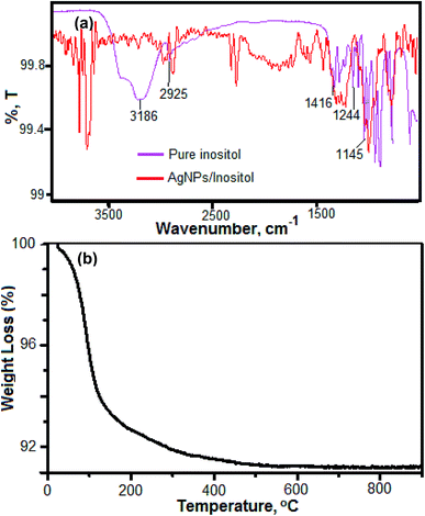 | ||
| Fig. 3 (a) FTIR spectra of Ag NPs/Ino before and after sintering and (b) TGA analysis of Ag NPs/Ino performed over the temperature range of 0 to 800 °C with an increase of 10 °C min−1. | ||
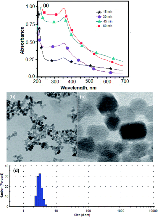
Similarly, the size of the ZnO NPs was established by measuring the LSPR absorption band with UV-vis. The LSPR absorption band at around 350 nm shows that the average size of the NPs was around 10–30 nm.38 The intense signal intensity of the absorption peak at 350 nm for 60 min of reaction time shows the optimum formation of the ZnO NPs and after no significant improvement was observed as shown in Fig. 4(a). This showed that the amount of NPs synthesized increased with increasing the reaction time from 15 min to 60 min and after no significant increase in concentration of NPs. Therefore, the maximum amount of NPs was produced when the reaction time was 60 min. Also the size and shape of the ZnO NPs were verified by TEM analysis as shown in Fig. 4(b) and (c). The TEM image and the enlarged view of the TEM image confirmed the average size of the ZnO NPs was about 12 ± 2.1 nm.39 Fig. 4(d) shows the percentage distribution for the size of the ZnO NPs using DLS measurement and a similar result was obtained as the TEM analysis.
Effect of solvent, stabilizer and concentration of NPs for preparation of a stable nano-ink
The prepared Ag NPs/Ino were dispersed in different solvents (DW, methanol, ethylene glycol and iso-propanol) in an ultrasonic bath for 10 min at room temperature. A uniform and stable ink was not formed with the use of these solvents and the NPs started to settle at the bottom after some time. This is due to the use of a small molecule, i.e. inositol as a capping agent for the stabilization of NPs which can remain stable at lower concentrations but not at higher concentrations.40,41 Therefore, 1% of PVP, PVA and chitosan was added as a stabilizer and stirred for 2 min to prevent the settling of the NPs. The Ag NPs/Ino dispersed in water showed better stability and dispersity, thus they were used further for the preparation of the ink. In addition, 1% glycerol was added as a wetting agent to the solution mixture. The results are given in Table S1 and Fig. S1.† Parameters such as polarity, viscosity, boiling point and surface tension were important parameters that were considered during the formulation of the stable ink. A stable silver nano-ink was obtained with aqueous solution because of the difference in dipole moments and polarity of NPs. The addition of a very small amount of polymer to this solution mixture caused a better stability of the prepared nano-ink. The ink was found to be stable up to five successive weeks with the addition of 1% of PVP to the solution mixture. However, the inks with PVP and chitosan showed better stability. This is due to the steric hindrance arising from the long-chain of PVP as well as the polarity and enhanced pi–pi interaction with the NPs and PVP providing a better stability to the conductive nano-ink.42 Finally, glycerol was added to the nano-ink solution to improve viscosity, moisture and surface tension to maintain the stability the NPs during the fabrication of the paper substrate. In addition, the concentration of Ag NPs/Ino was also optimized to acquire a better conductive surface on the substrate material. For this, different concentrations of NPs from 2 to 12% were dissolved in DW containing appropriate amounts of PVP and glycerol. A linear decrease in the resistance value was observed as the concentration of NPs increased to 10% and after there was no significant decrease in the resistance value. The reason for the decrease in resistance (increase in conductivity) with the increase in NP concentration is due to the formation of a uniform conductive layer of NPs on the paper substrate. Further, the increase in the concentration of NPs may not cause a significant increase in conductivity after acquiring an optimal value. Thus, 10% silver nano-ink was used for fabricating the paper substrates.32Effect of paper substrates for fabricating the silver nano-ink for making a conductive surface
Different paper such as filter paper, printing paper, photo paper, butter paper and bond paper were selected for the fabrication of paper based devices using silver nano-ink. For this, 10% silver nano-ink was fabricated on different paper substrates using a ball-point pen. The prepared conductive tracks were sintered at a particular temperature for a given time and the value of resistance was measured using a digital multimeter. The lowest value of resistance was obtained when the nano-ink was fabricated on photo paper. This is due to the homogenous coating of nano-ink on photo paper as well the fine pore size and moderate absorption of nano-ink within the cellulose fibers. However, filter papers, printing paper, photo paper, butter paper and bond paper have large pore sizes which caused trapping of the NPs into the fibers leading to discontinuity in the electronic track.34,43 Therefore, the photo paper substrate was used for direct writing of conductive using silver nano-ink.Effect of sintering temperature and sintering time for making a conductive surface
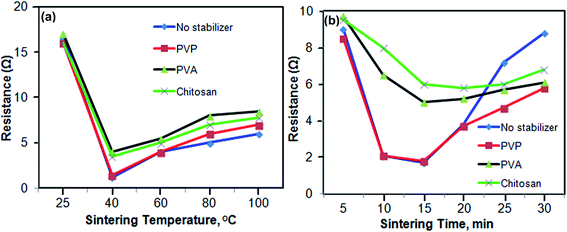
As we already know, sintering temperature and sintering time are found to be the most important parameters that affect the resistance of Ag NPs on the substrate materials. So, stability and resistance were tested by preparing conductive tracks with nano-ink using different stabilizers and varying the sintering temperatures from 25 to 100 °C for 15 min of sintering time. The results are shown in Table S2† and Fig. 5(a). The conductive track showed a high value of resistance at room temperature because of the presence of a high concentration of coating agents, stabilizers and solvent molecules around the Ag NPs/Ino. However, when the prepared conductive track was heated form 25 °C to 100 °C, there was a gradual decrease in the resistance value up to 40 °C. Further increasing the temperature up to 100 °C caused a gradual increase in the resistance value. This is due to the removal of some coating agents from the surface of NPs resulting in the welding of particles to form an uninterrupted layer of conductive surface as the temperature increased to 40 °C. After, further heating might not aid the formation of a continuous layer, instead it damages the paper substrate and thus all the experiments were performed at 40 °C.33,34The variation of sintering time also influences the resistance of NPs onto the photo paper substrate. For testing the effect of the change of sintering time on the resistance, the conductive track made of paper substrates with nano-ink was heated at 40 °C for different time intervals of 5, 10, 15, 20, 25 and 30 min. The results are shown in Table S3† and Fig. 5(b). A sintering time of 15 min was found to be best for accomplishing a lower value of resistance for three different types of nano-ink with different stabilizing agents. A lower value of resistance was obtained when PVP was used as a stabilizing agent for preparation of nano-ink and no significant decrease in the resistance was obtained after heating the substrate beyond 15 min.33 The low value of sintering temperature and time was found to be suitable for making a conductive substrate on a paper substrate for analytical and electronic applications.
Application of a fabricated electrode with silver nano-ink for electrochemical applications
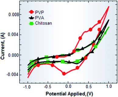
A paper fabricated electrode with Ag NPs/Ino was exploited as a working electrode in cyclic voltammetric (CV) measurements along with platinum and Ag/AgCl as the counter and reference electrodes, respectively (Metrohm Autolab, Netherland) in the presence of 0.1 M KNO3 as the electrolyte. The working electrodes were prepared with silver nano-ink using three different stabilizers (PVP, PVA and chitosan). The result is given in Fig. 6. The curve showing the oxidation and reduction current peaks corresponding to oxidation (Ag0 to Ag+) and reduction (Ag+ to Ag0) of Ag NPs/Ino. No specific peaks were obtained for the alcoholic and ketonic groups present in stabilizers, but their presence in the nano-ink influenced the current density of the peak. The response obtained by the paper based electrode prepared was found to be very similar to the response of the Ag NPs modified electrodes when used as a working electrode.44 This gives us the deliberation for using paper based electrodes as working electrodes in electroanalytical applications. A better CV response was obtained when PVP was used as a stabilizer for preparing the nano-ink because it supported the current densities. On the contrary, the other two stabilizers (PVA and chitosan) suppressed the current density of the prepared electrodes with their corresponding inks. In addition, paper based electrodes are easy, inexpensive, flexible and user-friendly to use in comparison with the conventional sophisticated electrodes made from glass materials and expensive metals such as platinum and gold. Also, the use of flexible paper based electrodes in CV measurements could certainly reduce the cost of analysis compared to conventional commercially available electrodes.Application of a paper based touch pad fabricated with ZnO NPs along with the conductive track of Ag NPs
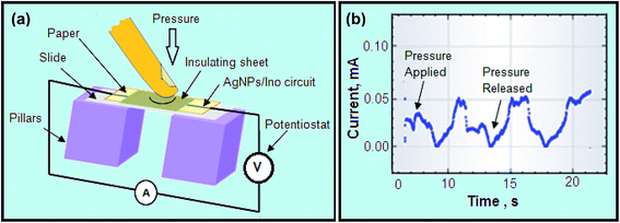
Next, the ZnO deposited on the paper substrate and connected with a silver conductive track was used as a touch pad, as shown in Fig. 7. The fabricated paper substrate with ZnO NPs was kept over supporting pillars which acted as a touch button to produce electric charges on the response of applied pressure. To build the device, ZnO fabricated paper was placed on the top of the pillars (acrylic substrate) separated from each other and adhesive tape covered the top of the button surface providing electrical insulation to the circuit, as shown in Fig. 7(a). The working principle of the paper based touch pad was demonstrated by measuring the piezoelectric current produced after applying mechanical stress on the deposited ZnO NPs. During the pressing, the ZnO NPs fabricated paper becomes deformed, followed by the generation of an electric charge against the applied mechanical stress. The silver electrodes prepared with conductive ink on the top of the ZnO NPs paper collect the generated electric charges followed by the measurement in amperometry, as shown in Fig. 7(b).During the operation, electric current was induced in ZnO fabricated paper by applying mechanical stress to the system. However, no current was observed while mechanical stress was not applied. A positive current peak at the milliampere level appeared while pressing the pad and disappeared upon the release of pressure.45,46 This is due to the release of the finger, the deformed paper is restored and generates a positive current peak. The basic cause for the generation of piezoelectricity is due to the interaction between the mechanical and electromechanical state of any material. When mechanical stress was applied on the static structure of the ZnO crystal, 0.1% deformation of material was caused, followed by a change in polarity of the system. Here, the generation of piezoelectric current is because of the two types of deformation: (a) that due to the deformation of the ZnO NPs on the touched area of the paper induced directly by a finger press; and (b) that due to the deformation of ZnO NPs on the untouched area of paper that were induced by deformation of the paper on which they were grown.8 Hence, paper fabricated with ZnO NPs on a paper substrate was successfully demonstrated for use in touch pad devices for electronic applications.
Conclusions
The present work demonstrated the fabrication of a paper electrode with Ag NPs/Ino, which was then used as a working electrode for electrochemical applications in cyclic voltammetry analysis. The paper electrode was prepared by the direct writing of nano-ink (10% Ag NPs in water and PVP) on photo paper and then sintering at 40 °C for 15 min. Further, the paper touch pad fabricated with ZnO was illustrated to show the piezoelectric effect reflexive to mechanical stress. In the near future, the preparation of paper based devices will help in designing touch pads for the development of compatible electronics. The use of a paper based electrode and touch pad was found to be simple, flexible, biodegradable, low cost and user-friendly for electrochemical and electronic applications compared to commercially available sophisticated electrodes and the expensive touch pads available.Conflicts of interest
There are no conflicts to declare.Acknowledgements
We would like to thank the Science and Engineering Research Board (SERB), New Delhi for awarding Kamlesh Shrivas an Extra Mural Research Project (File No: EMR/2016/005813).References
- X. Cao, H. Chen, X. Gu, B. Liu, W. Wang, Y. Cao, F. Wu and C. Zhou, ACS Nano, 2014, 8, 12769–12776 CrossRef CAS PubMed.
- R. Cao, X. Pu, X. Du, W. Yang, J. Wang, H. Guo, S. Zhao, Z. Yuan, C. Zhang, C. Li and Z. L. Wang, ACS Nano, 2018, 12, 5190–5196 CrossRef CAS PubMed.
- T. Chen, L. Qiu, Z. Cai, F. Gong, Z. Yang, Z. Wang and H. Peng, Nano Lett., 2012, 12, 2568–2572 CrossRef CAS PubMed.
- P. Sundriyal and S. Bhattacharya, ACS Appl. Mater. Interfaces, 2017, 9, 38507–38521 CrossRef CAS PubMed.
- H.-C. Chu, Y.-C. Chang, Y. Lin, S.-H. Chang, W.-C. Chang, G.-A. Li and H.-Y. Tuan, ACS Appl. Mater. Interfaces, 2016, 8, 13009–13017 CrossRef CAS PubMed.
- X. Wang, W.-Z. Song, M. You, J. Zhang, M. Yu, Z. Fan, S. Ramakrishna and Y. Long, ACS Nano, 2018, 12, 8588–8596 CrossRef CAS PubMed.
- M. Segev-Bar and H. Haick, ACS Nano, 2013, 7, 8366–8378 CrossRef CAS PubMed.
- X. Li, Y.-H. Wang, C. Zhao and X. Liu, ACS Appl. Mater. Interfaces, 2014, 6, 22004–22012 CrossRef CAS PubMed.
- A. D. Mazzeo, W. B. Kalb, L. Chan, M. G. Killian, J. F. Bloch, B. A. Mazzeo and G. M. Whitesides, Adv. Mater., 2012, 24, 2850–2856 CrossRef CAS PubMed.
- I. Chae, C. Kyu, J. Z. Ounaies and S. H. Kim, ACS Appl. Bio Mater., 2018, 1, 936–953 CrossRef CAS.
- A. Manekkathod, M. Y. Lu, C. W. Wang and L. J. Chen, Adv. Mater., 2010, 22, 4059–4063 CrossRef PubMed.
- S. Baruah, M. Jaisai, R. Imani, M. M. Nazhad and J. Dutta, Sci. Technol. Adv. Mater., 2010, 11, 055002 CrossRef PubMed.
- A. Sultana, Md. M. Alam, S. Garain, T. K. Sinha, T. Ranjan Middya and D. Mandal, ACS Appl. Mater. Interfaces, 2015, 7, 19091–19097 CrossRef CAS PubMed.
- C. Segarra, J. I. Climente, A. Polovitsyn, F. Rajadell, I. Moreels and J. Planelles, J. Phys. Chem. Lett., 2016, 7, 2182–2188 CrossRef CAS PubMed.
- P. Tyagi, R. R. Cooney, S. L. Sewall, D. M. Sagar, J. I. Saari and P. Kambhampati, Nano Lett., 2010, 10, 3062–3067 CrossRef CAS PubMed.
- N. P. Bacalzo Jr, L. P. Go, C. J. Querebillo, P. Hildebrandt, F. T. Limpoco and E. P. Enriquez, ACS Appl. Nano Mater., 2018, 1, 1247–1256 CrossRef.
- S. Magdassi, A. Bassa, Y. Vinetsky and A. Kamyshny, Chem. Mater., 2003, 15, 2208–2217 CrossRef CAS.
- N. N. Jason, W. Shen and W. Cheng, ACS Appl. Mater. Interfaces, 2015, 7, 16760–16766 CrossRef CAS PubMed.
- M. J. Rosemary and T. Pradeep, J. Colloid Interface Sci., 2003, 268, 81–84 CrossRef CAS.
- A. Pal, S. Shah and S. Devi, Mater. Chem. Phys., 2009, 114, 530–532 CrossRef CAS.
- M. G. Guzman, J. Dille and S. Godet, Int. J. Chem. Biomol. Eng., 2009, 2, 104–111 CAS.
- N. Duran, P. D. Marcato, O. L. Alves, G. I. Souza and E. Esposito, J. Nanobiotechnol., 2005, 3, 8 CrossRef PubMed.
- A. Kosmala, Q. Zhang, R. Wright and P. Kirby, Mater. Chem. Phys., 2012, 132, 788–795 CrossRef CAS.
- N. Zhang, J. Luo, R. Liu and X. Liu, RSC Adv., 2016, 6, 83720–83729 RSC.
- A. Zhu, L. Yuan and S. Dai, J. Phys. Chem. C, 2008, 112, 5432–5438 CrossRef CAS.
- T. Morioka, M. Takesue, H. Hayashi, M. Watanabe and R. L. Smith Jr, ACS Appl. Mater. Interfaces, 2016, 8, 1627–1634 CrossRef CAS.
- B. Huang, T. G. M. van de Ven and R. J. Hill, Langmuir, 2011, 27, 11416–11429 CrossRef CAS PubMed.
- D. Erath, A. Filipovic, M. Retzlaff, A. K. Goetz, F. Clement, D. Biro and R. Preu, Sol. Energy Mater. Sol. Cells, 2010, 94, 57–61 CrossRef CAS.
- W. J. Hyun, E. B. Secor, M. C. Hersam, C. D. Frisbie and L. F. Francis, Adv. Mater., 2015, 27, 109–115 CrossRef CAS.
- W. Wang and B. Gu, ACS Symposium Series, Chapter 1: Concentrated Dispersions, 2004, vol. 878, pp. 1–14 Search PubMed.
- S. Magdassi and M. Ben Moshe, Langmuir, 2003, 19, 939–942 CrossRef CAS.
- A. Ghosale, R. Shankar, V. Ganesan and K. Shrivas, Electrochim. Acta, 2016, 209, 511–520 CrossRef CAS.
- M. Sondergaard, E. D. Bojesen, M. Christensen and B. B. Iversen, Cryst. Growth Des., 2011, 11, 4027–4033 CrossRef.
- A. Ghosale, K. Shrivas, R. Shankar and V. Ganesan, Anal. Chem., 2017, 89, 776–782 CrossRef CAS PubMed.
- J. Saha, A. Begum, A. Mukherjee and S. Kumar, Environ. Res., 2017, 27, 245–250 CAS.
- P. K. Khanna, N. Singh, S. Charan, V. V. V. S. Subbarao, R. Gokhale and U. P. Mulik, Mater. Chem. Phys., 2005, 93, 117–121 CrossRef CAS.
- P. K. Rastogi, V. Ganesan and U. P. Azad, Electrochim. Acta, 2016, 188, 818–824 CrossRef CAS.
- L. Guo, S. Yang, C. Yang, P. Yu, J. Wang, W. Ge and G. K. L. Wong, Chem. Mater., 2000, 12, 2268–2274 CrossRef CAS.
- A. J. Morfa, B. C. Gibson, M. Karg, T. J. Karle, A. D. Greentree, P. Mulvaney and S. Tomljenovic-Hanic, Nano Lett., 2012, 12, 949–954 CrossRef CAS.
- N. Wang, H. F. Yang, X. Zhu, R. Zhang, Y. Wang, G. F. Huang and Z. R. Zhang, Nanotechnology, 2009, 20, 315603 (Inorg. Chem., 2014, 53, 7227–7232) CrossRef PubMed.
- X. Guo, Y. Fu, S. Fu, H. Wang, T. Yang, Y. Wen and H. Yang, Inorg. Chem., 2014, 53, 7227–7232 CrossRef CAS PubMed.
- M. Tejamaya, I. Romer, R. C. Merrifield and J. R. Lead, Environ. Sci. Technol., 2012, 46, 7011–7017 CrossRef CAS PubMed.
- G.-W. Huang, H.-M. Xiao and S.-Y. Fu, Nanoscale, 2014, 6, 8495–8502 RSC.
- F. Fathi, M. Schlitt, D. B. Pedersen and H.-B. Kraatz, Langmuir, 2011, 27, 12098–12105 CrossRef CAS.
- W. Lan, Y. Chen, Z. Yang, W. Han, J. Zhou, Y. Zhang, J. Wang, G. Tang, Y. Wei, W. Dou, Q. Su and E. Xie, ACS Appl. Mater. Interfaces, 2017, 9, 6644–6651 CrossRef CAS PubMed.
- E. Koenig, A. Jacobs and G. Lisensky, J. Chem. Educ., 2017, 94, 738–742 CrossRef CAS.
Footnote |
| † Electronic supplementary information (ESI) available. See DOI: 10.1039/c9ra02599e |
| This journal is © The Royal Society of Chemistry 2019 |

