
 Open Access Article
 This Open Access Article is licensed under a Creative Commons Attribution-Non Commercial 3.0 Unported Licence
Close-packed silane nanodot arrays by capillary nanostamping coupled with heterocyclic silane ring opening†
Michael Philippia,
Changjiang You*bc,
Christian P. Richterb,
Mercedes Schmidta,
Jannis Thiend,
Domenik Lißeb,
Joachim Wollschlägerd,
Jacob Piehler b and
Martin Steinhart*a
b and
Martin Steinhart*a
aInstitute for Chemistry of New Materials, Center for Cellular Nanoanalytics (CellNanOs), Universität Osnabrück, Barbarastr. 7, 49076 Osnabrück, Germany. E-mail: martin.steinhart@uos.de
bDepartment of Biology, Center for Cellular Nanoanalytics (CellNanOs), Universität Osnabrück, Barbarastr. 11, 49076 Osnabrück, Germany. E-mail: changjiang.you@biologie.uni-osnabrueck.de
cCollege of Life Sciences, Beijing University of Chemical Technology, 100029 Beijing, China
dDepartment of Physics, Universität Osnabrück, Barbarastr. 7, 49076 Osnabrück, Germany
First published on 9th August 2019
Abstract
We report the parallel generation of close-packed ordered silane nanodot arrays with nanodot diameters of few 100 nm and nearest-neighbor distances in the one-micron range. Capillary nanostamping of heterocyclic silanes coupled with ring-opening triggered by hydroxyl groups at the substrate surfaces yields nanodots consisting of silane monolayers with exposed terminal functional groups. Using spongy mesoporous silica stamps with methyl-terminated mesopore walls inert towards the heterocyclic silanes, we could manually perform multiple successive stamping cycles under ambient conditions without interruptions for ink refilling. Further functionalizations include the synthesis of polymer nanobrushes on the silane nanodots by surface-initiated atom-transfer radical polymerization. Proteins-of-interest fused to the HaloTag were site-specifically captured to silane nanodots functionalized by copper-free reactions with azide derivatives. Thus, bioorthogonal functionalization for bioanalytics with a spatial resolution in the one-micron range may be realized on solid supports compatible with fluorescence-based optical microscopy. The feature sizes of the silane nanodot arrays match well the length scales characteristic of a variety of biomolecular submicroscopic organizations in living cells, thus representing a compromise between miniaturization and the resolution limit of optical microscopy for sensitive high-throughput bioanalytics.
1 Introduction
Spatially controlled surface biofunctionalization at the micro- and nanoscale is a prerequisite for multiplexed bioanalytics, diagnostics and drug screening1,2 as well as for systematic exploration of the role of spatial protein organization in cell biology.3–5 Microcontact printing6,7 and polymer pen lithography8,9 combined with surface-initiated polymerization10–13 are often employed for chemical surface patterning, enabling, for example, reversible modulation of biointerfacial interactions14,15 and immobilization of biorecognition elements on protein-repellent polymer brushes.16 Simple patterns such as lines and squares are typically obtained by classical microcontact printing,17 whereas more complex patterns such as brush-polymer microarrays were obtained by polymer pen lithography.18,19 The deformability of the elastomeric stamps used for chemical surface pattering limits the attainable resolutions and nearest-neighbor distances.20,21 Reductions in the feature size require complex stamp configurations, such as composite stamps consisting of a harder contact surface connected to a softer support.22 Most importantly, contact-lithographic methods relying on solid elastomeric stamps do not allow for in situ supply of ink to the contact surfaces of the stamps without interruption of the stamping operations.Here we report the generation of ordered close-packed silane nanodot arrays with nanodot diameters of a few 100 nm and lattice constants in the one-micron range. To this end, we combined capillary nanostamping23,24 onto glass slides with the binding of heterocyclic silanes introduced by Kim et al. to the glass surface via ring-opening triggered by surface hydroxyl groups25,26 (Fig. 1). Nanobioanalytics by optical microscopy relies on monitoring of the fluorescence of analytes, probes, and labels. Direct attachment of heterocyclic silanes to hydroxyl-terminated substrate surfaces circumvents fluorescence quenching associated with classical thiol-on-gold chemistry. Moreover, on highly transparent glass substrates improved fluorescence signal-to-background contrast can be obtained. Hence, orthogonal biofunctionalization of the silane nanodots and the substrate areas surrounding them may yield substrates for sensitive high-throughput bioanalytics with micron-scale periodicity. Downscaling feature sizes on substrates for bioanalytics needs to be balanced with the need for reliable spatially resolved readout of processes of interest by optical microscopy. Arrays of silane nanodots with diameters of a few 100 nm and nearest-neighbor distances slightly above one micron represent a viable compromise between miniaturization and the resolution limit of optical microscopy. Furthermore, nearest-neighbor distances in the one-micron range match well the length scales characteristic of a variety of biomolecular submicroscopic organizations in living cells including membrane microcompartments, membrane-less organelles or protein phase separations27 that play crucial roles for cell signaling and metabolism. Protein arrays obtained by specific immobilization of proteins-of-interest on the silane nanodots are ideal tools for deciphering the composition and spatiotemporal organization of microcompartmentalization at subcellular levels. In this way, protein aggregates,28 liquid–liquid phase separation29 and lipid phase separation within plasma membrane microcompartments30 may be quantitatively assayed in living cells.
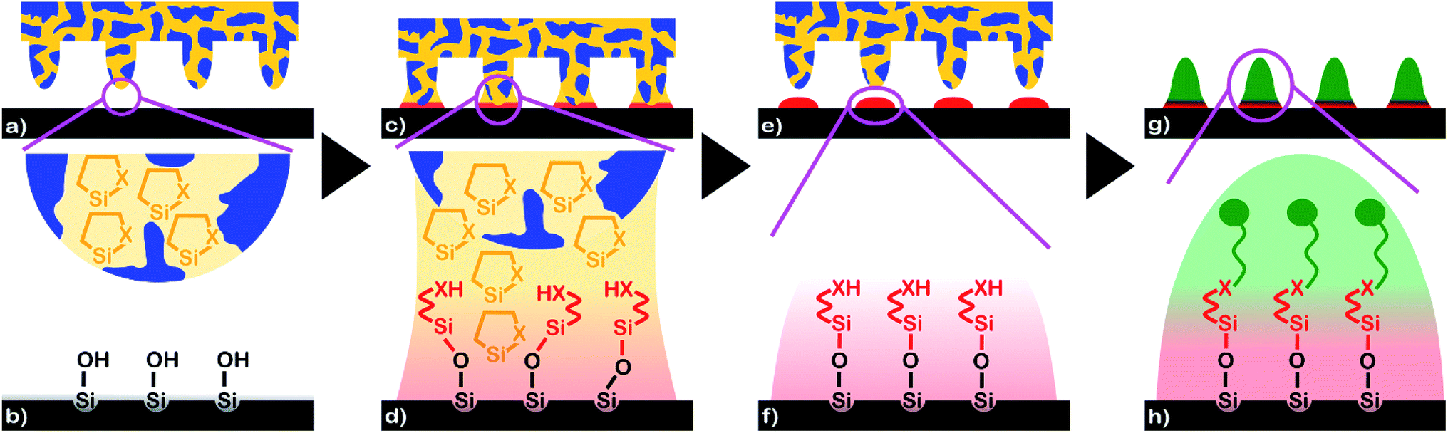 | ||
| Fig. 1 Generation of silane nanodot arrays by capillary nanostamping of heterocyclic silanes coupled with substrate-initiated ring opening. (a) and (b) A spongy mesoporous silica stamp (blue) soaked with ink containing heterocyclic silanes (orange; X = heteroatom) approaches a glass slide (black) with hydroxyl-terminated surface. (c) and (d) Liquid ink bridges form at the positions of the stamp's contact elements. The hydroxyl groups at the glass surface trigger ring opening of the heterocyclic silanes. (e) and (f) At the positions of the contact elements nanodots consisting of a silane monolayer (red) bound to the glass surface form without byproducts. (g) and (h) The exposed terminal XH groups of the substrate-bound silane molecules enable further functionalization of the silane nanodots. | ||
2 Experimental
2.1 Chemicals and materials
Dry toluene, dry dichloromethane (DCM), α-bromoisobutyryl bromide (BIBB), copper(II)bromide, N,N,N′,N′′,N′′-pentamethyldiethylenetriamine (PMTDA) and tin(II) 2-ethylhexanoate were purchased from Alfa Aesar. Styrene, ethyl-α-bromoisobutyrate (EBIB), triethylamine (TEA) dimethylformamide (DMF) and aminopropyltrimethoxysilane (APTMS) were obtained from Sigma Aldrich. N-Aminoethyl-aza-2,2-dimethyl-4-methylsilacyclopentane (thereafter referred to as cycloazasilane) and 2,2-dimethoxy-1-thia-2-silacyclopentane (thereafter referred to as cyclothiasilane) were purchased from Gelest. The fluorescent dyes ATTO 647 NHS and ATTO 655 maleimide were obtained from ATTO-TEC GmbH, Germany. Dibenzocyclooctyne-(polyethyleneglycol-12)-N-hydroxysuccinimidyl ester (NHS-PEG12-DBCO) was purchased from Click Chemistry Tools, USA. Azido-HaloTag-Ligand (click-HTL) was synthesized as described previously.31 The IUPAC name of click-HTL is 3-(4-azidophenyl)-N-(2-(2-(6-chlorohexyloxy)ethoxy)ethyl)propanamide. HaloTag-fused monomeric enhanced GFP protein (HaloTag-mEGFP) and poly(L-lysine)-graft-poly(ethylene glycol) terminated with methoxy groups (PLL-PEG-OMe) were prepared according protocols described previously.32,33 Chemicals for preparing HEPES buffered saline (HBS), such as 4-(2-hydroxyethyl)-1-piperazineethanesulfonic acid and NaCl were purchased from Sigma Aldrich.2.2 Capillary nanostamping
Spongy silica stamps with an area of 5 × 5 mm2 and a thickness of 3 mm were prepared following procedures reported elsewhere.23 The spongy silica stamps were immersed into toluene and then into the ink for ∼15 min. We used a 0.5 mM solution of the cycloazasilane, a 2 mM solution of the cyclothiasilane and a 2 mM APTMS solution in dry toluene as inks.The glass slides to be stamped were treated with oxygen plasma for 10 min using a Diener femto plasma cleaner. The ink-infiltrated spongy silica stamps were attached to stamp holders with double-sided adhesive tape. As stamp holders we used stainless steel cylinders (height 4.5 cm; diameter 2 cm; mass ∼ 27 g) with a flat cylinder base and an additional 3 mm thick poly(dimethylsiloxane) (PDMS) layer between stamp and base. After capillary nanostamping, the patterned glass slides were rinsed with toluene and ethanol to remove unreacted silane molecules. Silane nanodots obtained by capillary nanostamping of cycloazasilane are thereafter referred to as aminosilane nanodots and silane nanodots obtained by capillary nanostamping of cyclothiasilane as thiosilane nanodots.
2.3 Post-stamping treatments
2.4 Characterization
3 Results and discussion
3.1 Capillary nanostamping of heterocyclic silanes: principle
Classical agents for surface modification – such as trifunctional alkoxysilanes, carboxysilanes and chlorosilanes – undergo hydrolytic condensation and are prone to polymerization triggered by water. Polymerization may occur close to and away from a substrate surface to be modified.36 Monofunctional and bifunctional noncyclic silanes, on the other hand, frequently lack the required reactivity. We used inks containing heterocyclic silanes that have recently emerged as a new class of agents for highly precise modification of hydroxyl-terminated surfaces. Cyclic azasilanes containing Si–N bonds and cyclic thiosilanes containing Si–S bonds in their rings undergo click-chemical ring-opening reactions triggered by –OH groups on silica surfaces.25,26 The ring-opening is coupled with hydrogen transfer from the surface hydroxyl groups to the heteroatom X of the heterocyclic silanes. As a result, precisely one heterocyclic silane molecule per surface hydroxyl group will bind to the substrate surface. Polymerization of the heterocyclic silanes is intrinsically not possible. We moreover assume that heterocyclic silane molecules react with residual water the ink may contain. The heterocyclic silanes themselves thus remove water from the ink, while the resulting hydrolysis products do not bind to the silica surface or impede the surface-initiated ring-opening of the remaining heterocyclic silane molecules. Hence, silane monolayers having exposed terminal –XH groups form without byproducts.Capillary nanostamping was carried out with spongy mesoporous silica stamps prepared via the sol–gel route following procedures reported elsewhere23,37 using methyltrimethoxysilane37 as silica precursor. The spongy mesoporous silica stamps had methyl-terminated pore walls resistant against organic solvents and inert towards the heterocyclic silanes. Their contact surfaces were topographically patterned with regular hexagonal arrays of conical contact elements (base diameter ∼ 600 nm; tip diameter ∼ 400 nm; height ∼ 500 nm; nearest neighbour distance 1.2–1.3 μm; average pore diameter ∼ 31 nm) (cf. ESI Fig. S1† and ref. 23).
We infiltrated the spongy mesoporous silica stamps with solutions of the heterocyclic silanes in toluene and glued them onto cylindrical stamp holders. Capillary nanostamping with a contact time of less than 1 s was performed manually and under ambient conditions by bringing the topographically patterned contact surfaces of the spongy mesoporous silica stamps in contact with the surfaces of glass slides (Fig. 1a and b; for a photograph see ESI Fig. S2†). Ring opening by a reaction with the surface hydroxyl groups converted the heterocyclic silanes into XH-terminated non-cyclic alkyl silanes bound to the surfaces of the glass slides at the positions of the stamps' contact elements (Fig. 1c and d). As a result, nanodots with diameters of a few 100 nm consisting of silane monolayers form at the positions of the stamps' contact elements (Fig. 1e and f). Since the spongy mesopore system acts as ink reservoir and allows in situ ink supply, multiple successive stamping cycles can be performed under ambient conditions without interruptions for re-inking and without deterioration of the pattern quality. It should be noted that, in contrast to typical procedures used for polymer pen lithography, each single contact between a mesoporous silica stamp and a substrate already yields a complete silane nanodot array with a nearest-neighbour distance in the 1 μm range. A series of capillary nanostamping cycles carried out at different positions on a substrate or on different substrates yields, therefore, the corresponding number of separate silane nanodot arrays. The exposed terminal –XH groups of the silane molecules forming the nanodots enable further functionalization (Fig. 1g and h).
3.2 Capillary nanostamping of heterocyclic silanes: results
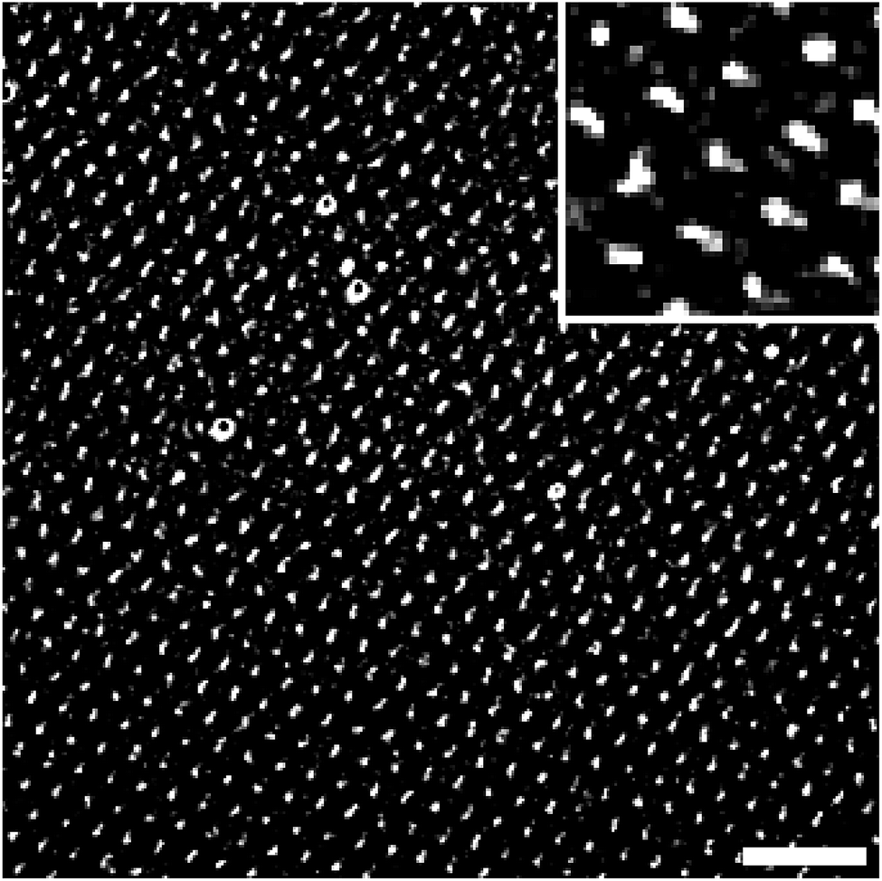
Stamping the cycloazasilane N-aminoethyl-aza-2,2-dimethyl-4-methylsilacyclopentane (X = N–CH2–CH2–NH2) in toluene onto glass slides resulted in the formation of [N-(2-aminoethyl)-2-methyl-3-aminopropyl]dimethylsilane nanodots (aminosilane nanodots) at the contact sites of the spongy mesoporous silica stamps by the ring-opening reaction sketched in Fig. 2a. A phenomenological signature of the presence of aminosilane nanodot arrays is an increase in the water contact angle, which amounts to 0° on unmodified glass slides. We measured the water contact angle on three aminosilane nanodot arrays that were successively stamped without reinking the mesoporous silica stamp and obtained water contact angles of 70.7°, 72.1° and 73.3°.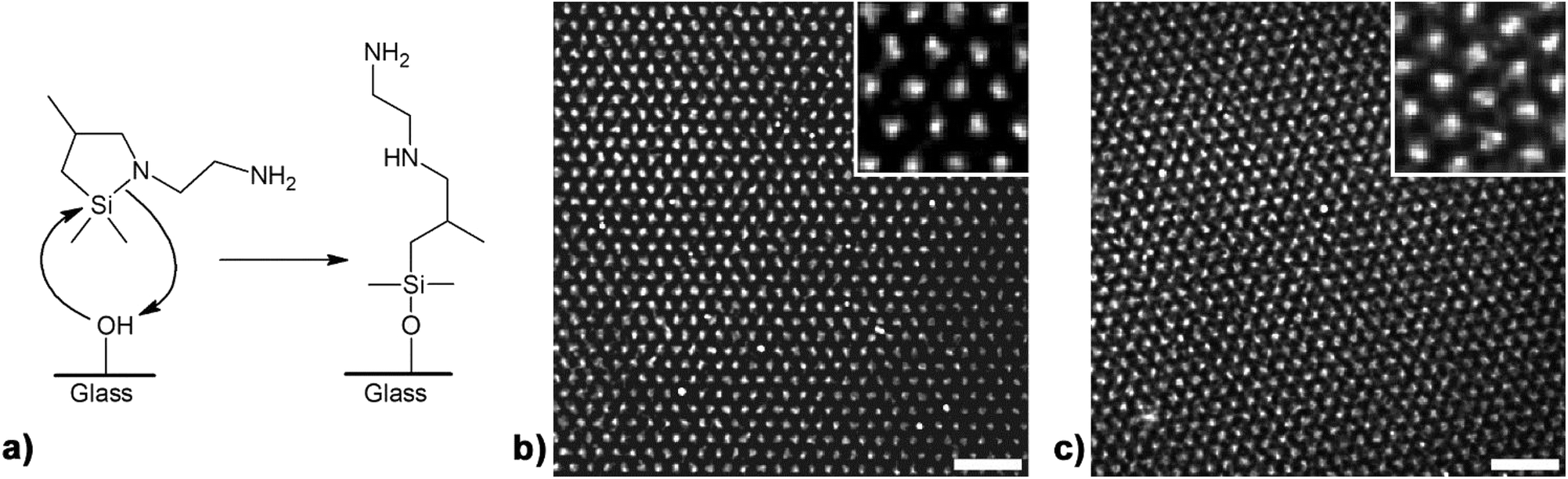 | ||
| Fig. 2 Capillary nanostamping of N-aminoethyl-aza-2,2-dimethyl-4-methylsilacyclopentane in toluene onto glass slides. (a) Reaction scheme of the ring opening reaction with the surface hydroxyl groups. (b) and (c) TIRFM images of aminosilane nanodot arrays stamped onto glass slides after binding the dye ATTO 647 NHS to the terminal amine groups of the silanes. (b) 4th and (c) 10th consecutive stamping cycle under ambient conditions without reinking. The raw TIRFM images were deconvolved using the Huygens software. The scale bars correspond to 5 μm. Insets are zoom-in regions of 5 × 5 μm2. | ||
XPS is frequently used to characterize silane layers on solid substrates. Thus, we measured XP spectra of areas in which the glass slides were patterned with aminosilane nanodot arrays and, for comparison, of nonpatterned areas in between. We acquired the XP spectra varying the take-off angle to distinguish contributions from the silica substrates and from the aminosilane nanodot arrays. Here, we present XP spectra obtained with a low electron take-off angle of 15° in order to enhance the surface sensitivity of the XPS measurements. The Si 2p peak of Si atoms incorporated into silica networks, which is attributed to Si in the oxidation state 4+, appears at a binding energy (BE) of ∼103.5 eV.38,39 In XP spectra of nonpatterned areas covering the corresponding BE region (ESI Fig. S3a†), a Si 2p peak with a maximum at 103.3 eV is detected that can be ascribed to silica-Si. The Si 2p peak originating from silane-Si has a maximum shifted to slightly lower BE values of 102.3–102.5 eV, since silane-Si is in the lower oxidation state 3+.38,39 If silanes on a silica surface are probed, the position of the Si 2p peak maximum lies between the positions of the peak maxima originating from silica-Si and from silane-Si.40 The XP spectrum seen in ESI Fig. S3b† was measured on an aminosilane nanodot array, which was located on the same glass slide as the nonpatterned area of which the XP spectrum seen in ESI Fig. S3a† was taken. The slight shift of the Si 2p peak maximum to a lower BE value of 102.9 eV in the XP spectrum of the aminosilane nanodot array indicates the presence of silane-Si. We decomposed the Si 2p peak obtained on the aminosilane nanodot array into two Lorentzian functions representing the contributions of silica-Si and silane-Si. The peak maximum of the silica-Si contribution was set to 103.3 eV, corresponding to the maximum of the Si 2p peak obtained for nonpatterned glass. The relative peak area of the silica-Si contribution amounted to 60%. The silane-Si contribution had a peak maximum at 102.5 eV and a relative peak area of 40%. However, the Lorentzian fits should be considered rather as a rough approach to the atomic number ratio silica-Si/silane-Si than as a precise determination of the latter due to the unknown escape depth of the photoelectrons from the silica substrates and the aminosilane nanodot arrays. We also recorded XP spectra in the BE region where the nitrogen 1s peak is located. While no indication for the presence of nitrogen was apparent in the XP spectrum recorded on nonpatterned glass, a N 1s peak at ∼400.5 eV originating from the aminosilane nitrogen atoms is clearly present in the XP spectrum of the aminosilane nanodot array (ESI Fig. S4†). Finally, the C 1s peak obtained from the aminosilane nanodot array shows, in contrast to the C 1s peak originating from adventitious carbon in the non-patterned area (with a binding energy of 185.0 eV), a shoulder at the higher-BE side (ESI Fig. S5a†). We fitted the sum of two Lorentzian contributions to the C 1s peak obtained from the aminosilane nanodot array (ESI Fig. S5b†). We assumed that the maximum of the C 1s peak originating from aminosilane methyl and methylene carbon atoms away from the more electronegative binding partner nitrogen equals the C 1s peak maximum obtained for adventitious carbon in the nonpatterned area. The second contribution shifted to higher BE values (peak maximum at 286.7 eV) can be ascribed to methylene carbon atoms in α-position to one of the amino groups.41 An aminosilane molecule contains 3 carbon atoms directly bound to nitrogen (38%) and 5 carbon atoms not bound to nitrogen (62%). The relative peak area of the Lorentzian function at higher BE values amounts to 28% and that of the Lorentzian function at lower BE values to 72%. Considering that adventitious carbon may contribute to the Lorentzian function at lower BE values, this peak area ratio is in reasonable agreement to the atomic number ratio. Overall, the results of the contact angle and XPS measurements corroborate the notion that the cycloazasilane molecules bind to the glass substrates during capillary nanostamping.
3.3 Dye-labelled aminosilane nanodot arrays: TIRFM
Arrays of aminosilane nanodots were further functionalized by attaching the dye ATTO 647 NHS to the terminal amine groups of the aminosilanes (Fig. 2a) and then imaged by TIRFM. The feature sizes of the silane nanodot arrays were not properly resolved in the raw images (ESI Fig. S6†) due to diffraction limitation. Therefore, we deconvolved the raw TIRFM images using the Huygens image processing software that takes the point spread function of the microscope into account. Deconvolved images of ATTO 647 NHS-functionalized aminosilane nanodot arrays obtained in the 4th and the 10th successive stamping cycles without reloading the spongy mesoporous silica stamp with ink are shown in Fig. 2b and c, respectively. The diameters of the aminosilane nanodots were determined from the deconvolved images by fitting isotropic 2D-Gaussians.35 For the 4th consecutive stamping cycle (Fig. 2b) we obtained a median nanodot diameter of 356 nm ± 51 nm and a nearest neighbour median distance of 1.31 μm ± 0.02 μm. For the 10th consecutive stamping cycle (Fig. 2c), we obtained a median nanodot diameter of 376 nm ± 60 nm and a nearest neighbour median distance of 1.30 μm ± 0.02 μm. Capillary nanostamping of 2,2-dimethoxy-1-thia-2-silacyclopentane onto glass slides correspondingly yielded arrays of dimethoxy-(3-thiopropyl)silane nanodots (ESI Fig. S7†). TIRFM imaging after binding the dye ATTO 655 maleimide to the terminal thiol groups yielded median nanodot diameters of 314 nm ± 58 nm (1st stamping cycle), 318 nm ± 52 nm (4th stamping cycle), 334 nm ± 64 nm (7th stamping cycle) and 342 nm ± 60 nm (10th stamping cycle).We could typically perform more than 10 successive stamping cycles under ambient conditions without reloading the spongy mesoporous silica stamps with ink and without deterioration of the quality of the generated silane nanodot arrays. Capillary nanostamping of heterocyclic silanes, even when carried out manually under ambient conditions, is robust with respect to variations in contact time and contact pressure. Within a series of 10 successive stamping cycles the nanodot median diameter typically scatters by ±5%. A reason for this robustness – as compared to manual stamping with elastomeric stamps – might be the rigidity of the contact elements of the mesoporous silica stamps. While the contact elements of elastomeric stamps consisting of materials such as cross-linked PDMS may deform upon contact formation with the substrate, the contact elements of the mesoporous silica stamps retain their shape. It should be noted that under the well-controlled conditions of polymer pen lithography (controlled atmosphere, parallel adjustment of stamp and substrate, controlled load during stamping) more precise control over pattern sizes is achievable.42 We assume that the nanodot size depends first and foremost on the geometry of the stamp's contact elements, which crucially affects the interplay of contact line movement of the liquid ink bridges at the contact elements, solvent evaporation and adsorption of the non-volatile ink components on the substrate. If, for example, mesoporous stamps with regular arrays of wells are used, correspondingly ordered holey films of the non-volatile ink components are obtained.43
Capillary nanostamping of “classical” trifunctional silane coupling agents – while, in principle, possible – may suffer from oligo- and polymerization of the silanes. For example, we stamped the trifunctional alkoxysilane APTMS under ambient conditions onto glass slides and bound ATTO 647 NHS to the terminal APTMS amino groups. The first stamping cycle yielded a regular array of APTMS nanodots with a median diameter of 298 nm ± 20 nm and a nearest neighbour median distance of 1.397 μm ± 10 nm (ESI Fig. S8a†). However, in the following stamping cycles carried out immediately thereafter the quality of the obtained patterns markedly deteriorated. In the TIRFM image of the pattern resulting from the fourth successive stamping cycle shown in ESI Fig. S8b,† only 9 features met the quality criteria for APTMS nanodots (cf. Section 2.4.6). Hence, we could not determine the median values of the nanodot diameter and nearest neighbour distance.
3.4 Chemical functionalization of aminosilane nanodots
The terminal functional groups of the silane molecules forming the nanodots also enable more complex chemical functionalizations (Fig. 3). For a proof-of-concept, we synthesized polystyrene (PS) brushes at the positions of the aminosilane nanodots by adapting protocols reported by Li et al.44 based on surface-initiated atom-transfer radical polymerization (ATRP) combined with a process referred to as “activators regenerated by electron transfer” (ARGET)45 (Fig. 3a–c). We coupled α-bromoisobutyryl bromide (BIBB) to the terminal amine groups of the aminosilane nanodots (Fig. 3b) to generate initiation sites for the synthesis of PS (Fig. 3c). Thus, we obtained regular large-area arrays of discrete PS nanobrushes (Fig. 4a and b, for larger-area SEM images see ESI Fig. S9†). The PS nanobrushes had diameters of ∼600 nm and heights of ∼15 nm, as determined from AFM topography images (Fig. 4c and d). No backfilling was necessary to obtain the arrays of PS nanobrushes.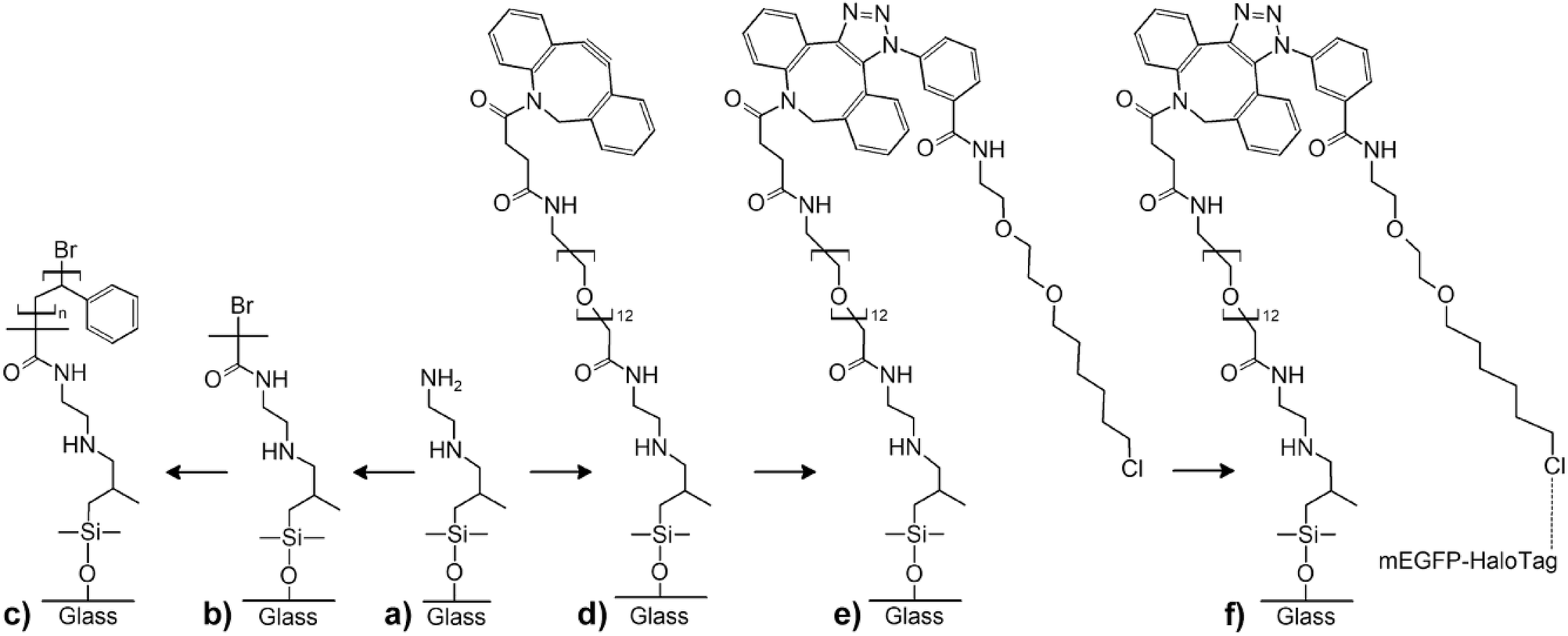 | ||
| Fig. 3 Functionalization of aminosilane nanodots. (a)–(c) Reaction scheme for the synthesis of PS nanobrushes at the positions of the aminosilane nanodots. (d)–(f) Reaction scheme for the functionalization of the aminosilane nanodots with HaloTag-fused monomeric enhanced green fluorescence protein. | ||
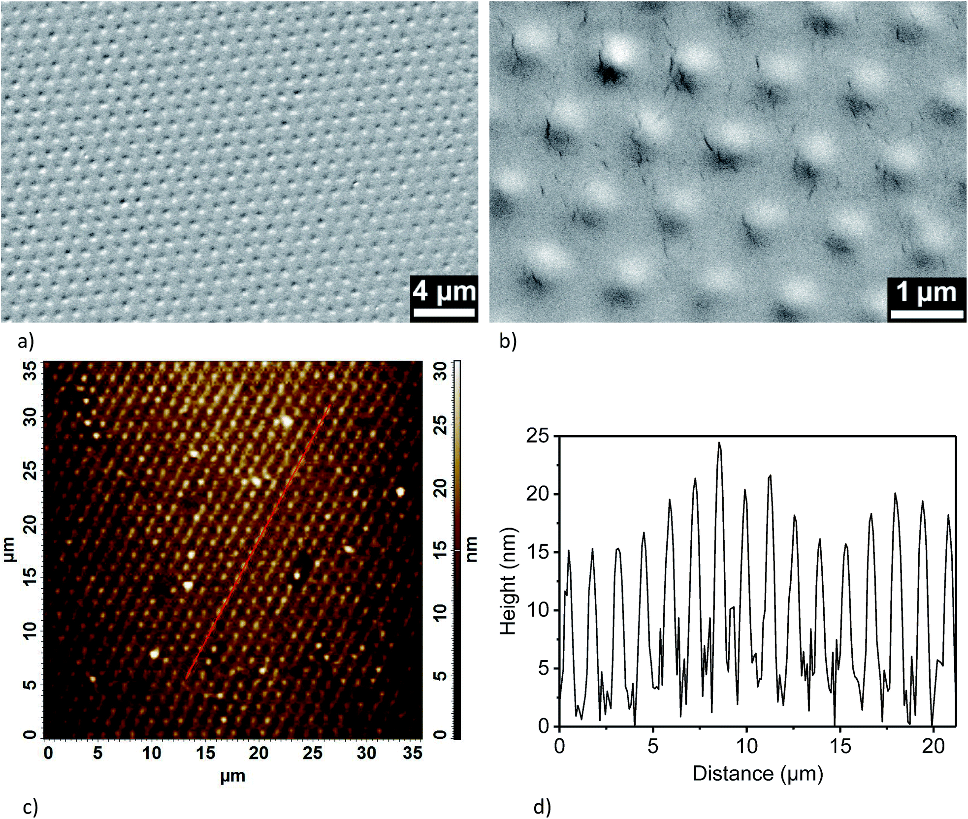 | ||
| Fig. 4 Functionalization of aminosilane nanodot arrays with PS nanobrushes via ARGET ATRP. (a) and (b) SEM images of an array of PS nanobrushes. (a) Overview; (b) detail. (c) AFM image of the topography of a PS nanobrush array. (d) Topographic profile along the line in panel (c). | ||
We could also demonstrate bio-orthogonal functionalization with an about tenfold improved spatial resolution as compared to conventional soft lithography for biofunctionalization32,46,47 by site-specific protein immobilization at the aminosilane nanodots via the HaloTag (Fig. 3a and d–f). Aminosilane nanodots were first reacted with dibenzocyclooctyne (DBCO)-NHS (Fig. 3d) and subsequently functionalized with azido-HaloTag-Ligand (click-HTL)31 by copper-free click chemistry (Fig. 3e). After backfilling with PLL-PEG-OMe to inhibit nonspecific protein binding around the aminosilane nanodots, monomeric enhanced green fluorescent protein fused to the HaloTag (HaloTag-mEGFP)32,33 was immobilized on the click-HTL-functionalized aminosilane nanodots (Fig. 3f). Surface binding of HaloTag-mEGFP to click-HTL was calculated using a pseudo-first order model according to Γ = 1 − e−konCt, where Γ is the surface load of HaloTag-mEGFP, C the concentration of HaloTag-mEGFP in solution and t the incubation time. We set the on-rate constant of HaloTag-mEGFP binding to click HTL kon to the previously determined value of 4 × 10⁴ M−1 s−1.31 The HaloTag-mEGFP concentration and the incubation time applied here ensured 91% click-HTL binding with HaloTag-mEGFP protein, as confirmed by TIRFM imaging (ESI Fig. S10†). The deconcolved TIRFM image shown in Fig. 5 contains an array bright aminosilane nanodots functionalized with HaloTag-mEGFP marked by mEGFP fluorescence. The aminosilane nanodots functionalized with HaloTag-mEGFP had an apparent median diameter of 220 nm ± 38 nm and a nearest-neighbour spacing of 1.32 μm.
 | ||
| Fig. 5 TIRFM image of an aminosilane nanodot array functionalized with Halo-Tag®/mEGFP showing mEGFP fluorescence. The raw TIRFM image was deconvolved using the Huygens software (scale bar = 5 μm; the inset is a zoom-in region of 5 × 5 μm2). | ||
4 Conclusions
In conclusion, the combination of manual capillary nanostamping under ambient conditions using spongy mesoporous silica stamps and lithographic surface modification via surface-initiated ring opening of heterocyclic silanes yielded close-packed arrays of discrete functionalizable silane nanodots with diameters of a few 100 nm and nearest-neighbour distances of 1.2–1.3 μm. These geometric array parameters match well the length scales characteristic of a variety of biomolecular submicroscopic organizations in living cells and represent a compromise between miniaturization and the resolution limit of optical microscopy. Since the stamps' spongy mesopore systems act as ink reservoir and can be used for in situ ink supply, multiple successive stamping cycles can be carried out without interruptions caused by ink depletion. The heterocyclic silanes bind to the surfaces of glass slides at the positions of the stamps' contact elements via ring opening triggered by the surface hydroxyl groups. Thus, the silane nanodots consisted of monolayers of silane molecules with exposed functional groups for further functionalization. Exemplary functionalizations of the silane nanodots included the generation of arrays of polymer nanobrushes by surface-initiated ATRP and the immobilization of proteins via conjugation of dibenzocyclooctyne to the silane nanodots to enable copper-free click reactions with azide derivatives. Avoiding gold substrates that impede fluorescence emission, the configuration reported here potentially enables orthogonal biofunctionalization for fluorescence-based nanobioanalytics combined with spatial resolutions in the one-micron range. The obtained 10-fold-improved spatial resolution in comparison to conventional micropatterned bioanalytic arrays results in an increase in the areal density of discrete cell–substrate interaction sites by two orders of magnitude.Conflicts of interest
There are no conflicts to declare.Acknowledgements
The authors thank the European Research Council (ERC-CoG-2014, project 646742 INCANA) for funding. C. Y. thanks the National Science Foundation of China (31870976) for support. TIRF microscopy and image analysis was supported by the DFG-funded Integrated Bioimaging Facility Osnabrück (PI 405/14-1).Notes and references
- D. Weinrich, P. Jonkheijm, C. M. Niemeyer and H. Waldmann, Angew. Chem., Int. Ed., 2009, 48, 7744–7751 CrossRef CAS PubMed.
- S. Schumacher, S. Muekusch and H. Seitz, Microarrays, 2015, 4, 196–213 CrossRef CAS PubMed.
- H. Cai, J. Muller, D. Depoil, V. Mayya, M. P. Sheetz, M. L. Dustin and S. J. Wind, Nat. Nanotechnol., 2018, 13, 610–617 CrossRef CAS PubMed.
- T. Satav, J. Huskens and P. Jonkheijm, Small, 2015, 11, 5184–5199 CrossRef CAS PubMed.
- V. Hortiguela, E. Larranaga, F. Cutrale, A. Seriola, M. Garcia-Diaz, A. Lagunas, J. Andilla, P. Loza-Alvarez, J. Samitier, S. Ojosnegros and E. Martinez, Nano Lett., 2018, 18, 629–637 CrossRef CAS PubMed.
- G. M. Whitesides, E. Ostuni, S. Takayama, X. Y. Jiang and D. E. Ingber, Annu. Rev. Biomed. Eng., 2001, 3, 335–373 CrossRef CAS PubMed.
- Y. Xia and G. M. Whitesides, Annu. Rev. Mater. Sci., 1998, 28, 153–184 CrossRef CAS.
- F. Huo, Z. Zheng, G. Zheng, L. R. Giam, H. Zhang and C. A. Mirkin, Science, 2008, 321, 1658–1660 CrossRef CAS PubMed.
- C. Carbonell and A. B. Braunschweig, Acc. Chem. Res., 2017, 50, 190–198 CrossRef CAS PubMed.
- I. W. Moran, J. R. Ell and K. R. Carter, Small, 2011, 7, 2669–2674 CrossRef CAS PubMed.
- B. Li, B. Yu, Q. Ye and F. Zhou, Acc. Chem. Res., 2015, 48, 229–237 CrossRef CAS PubMed.
- Q. Yu, L. K. Ista, R. P. Gu, S. Zauscher and G. P. Lopez, Nanoscale, 2016, 8, 680–700 RSC.
- W. L. Chen, R. Cordero, H. Tran and C. K. Ober, Macromolecules, 2017, 50, 4089–4113 CrossRef CAS.
- Q. Yu, P. Shivapooja, L. M. Johnson, G. Tizazu, G. J. Leggett and G. P. Lopez, Nanoscale, 2013, 5, 3632–3637 RSC.
- Q. Yu, J. Cho, P. Shivapooja, L. K. Ista and G. P. Lopez, ACS Appl. Mater. Interfaces, 2013, 5, 9295–9304 CrossRef CAS PubMed.
- U. Bog, A. D. Pereira, S. L. Mueller, S. Havenridge, V. Parrillo, M. Bruns, A. E. Holmes, C. Rodriguez-Emmenegger, H. Fuchs and M. Hirtz, ACS Appl. Mater. Interfaces, 2017, 9, 12109–12117 CrossRef CAS PubMed.
- T. Pompe, A. Fery, S. Herminghaus, A. Kriele, H. Lorenz and J. P. Kotthaus, Langmuir, 1999, 15, 2398–2401 CrossRef CAS.
- S. D. Bian, S. B. Zieba, W. Morris, X. Han, D. C. Richter, K. A. Brown, C. A. Mirkin and A. B. Braunschweig, Chem. Sci., 2014, 5, 2023–2030 RSC.
- Z. Xie, C. J. Chen, X. C. Zhou, T. T. Gao, D. Q. Liu, Q. Miao and Z. J. Zheng, ACS Appl. Mater. Interfaces, 2014, 6, 11955–11964 CrossRef CAS PubMed.
- A. Perl, D. N. Reinhoudt and J. Huskens, Adv. Mater., 2009, 21, 2257–2268 CrossRef CAS.
- J. L. Hedrick, K. A. Brown, E. J. Kluender, M. D. Cabezas, P. C. Chen and C. A. Mirkin, ACS Nano, 2016, 10, 3144–3148 CrossRef CAS PubMed.
- M. A. Verschuuren, M. Megens, Y. Ni, H. van Sprang and A. Polman, Adv. Opt. Technol., 2017, 6, 243–264 CAS.
- M. Schmidt, M. Philippi, M. Münzner, J. M. Stangl, R. Wieczorek, W. Harneit, K. Müller-Buschbaum, D. Enke and M. Steinhart, Adv. Funct. Mater., 2018, 28, 1800700 CrossRef.
- W. Han, P. Hou, S. Sadaf, H. Schäfer, L. Walder and M. Steinhart, ACS Appl. Mater. Interfaces, 2018, 10, 7451–7458 CrossRef CAS PubMed.
- D. Kim, J. M. Zuidema, J. Kang, Y. Pan, L. Wu, D. Warther, B. Arkles and M. J. Sailor, J. Am. Chem. Soc., 2016, 138, 15106–15109 CrossRef CAS PubMed.
- Y. L. Pan, A. Maddox, T. Min, F. Gonzaga, J. Goff and B. Arkles, Chem.–Asian J., 2017, 12, 1198–1203 CrossRef CAS PubMed.
- S. Boeynaems, S. Alberti, N. L. Fawzi, T. Mittag, M. Polymenidou, F. Rousseau, J. Schymkowitz, J. Shorter, B. Wolozin, L. Van Den Bosch, P. Tompa and M. Fuxreiter, Trends Cell Biol., 2018, 28, 420–435 CrossRef CAS PubMed.
- G. Simic, M. Babic Leko, S. Wray, C. Harrington, I. Delalle, N. Jovanov-Milosevic, D. Bazadona, L. Buee, R. de Silva, G. Di Giovanni, C. Wischik and P. R. Hof, Biomolecules, 2016, 6, 6 CrossRef PubMed.
- S. Ambadipudi, J. Biernat, D. Riedel, E. Mandelkow and M. Zweckstetter, Nat. Commun., 2017, 8, 275 CrossRef PubMed.
- A. Honigmann and A. Pralle, J. Mol. Biol., 2016, 428, 4739–4748 CrossRef CAS PubMed.
- D. Liße, V. Wilkens, C. You, K. Busch and J. Piehler, Angew. Chem., Int. Ed., 2011, 50, 9352–9355 CrossRef PubMed.
- T. Wedeking, S. Löchte, C. P. Richter, M. Bhagawati, J. Piehler and C. You, Nano Lett., 2015, 15, 3610–3615 CrossRef CAS PubMed.
- T. Wedeking, S. Löchte, O. Birkholz, A. Wallenstein, J. Trahe, J. Klingauf, J. Piehler and C. You, Small, 2015, 11, 5912–5918 CrossRef CAS PubMed.
- T. L. Barr and S. Seal, J. Vac. Sci. Technol., A, 1995, 13, 1239–1246 CrossRef CAS.
- A. Serge, N. Bertaux, H. Rigneault and D. Marguet, Nat. Methods, 2008, 5, 687–694 CrossRef CAS PubMed.
- S. Onclin, B. J. Ravoo and D. N. Reinhoudt, Angew. Chem., Int. Ed., 2005, 44, 6282–6304 CrossRef CAS PubMed.
- K. Kanamori, M. Aizawa, K. Nakanishi and T. Hanada, Adv. Mater., 2007, 19, 1589–1593 CrossRef CAS.
- K. M. R. Kallury, J. D. Brennan and U. J. Krull, Anal. Chem., 1995, 67, 2625–2634 CrossRef CAS.
- Y. C. Araujo, P. G. Toledo, V. Leon and H. Y. Gonzalez, J. Colloid Interface Sci., 1995, 176, 485–490 CrossRef CAS.
- T. J. Horr and P. S. Arora, Colloids Surf., A, 1997, 126, 113–121 CrossRef CAS.
- X. P. Cao and R. J. Hamers, J. Vac. Sci. Technol., B: Microelectron. Nanometer Struct.--Process., Meas., Phenom., 2002, 20, 1614–1619 CrossRef CAS.
- X. Liao, A. B. Braunschweig, Z. Zheng and C. A. Mirkin, Small, 2010, 6, 1082–1086 CrossRef CAS PubMed.
- L. Guo, M. Philippi and M. Steinhart, Small, 2018, 14, 1801452 CrossRef PubMed.
- Y. M. Li, Q. Li, C. Q. Zhang, P. Cai, N. N. Bai and X. Xu, Chem. Eng. J., 2017, 323, 134–142 CrossRef CAS.
- K. Matyjaszewski, H. C. Dong, W. Jakubowski, J. Pietrasik and A. Kusumo, Langmuir, 2007, 23, 4528–4531 CrossRef CAS PubMed.
- K.-i. Arimoto, S. Löchte, S. A. Stoner, C. Burkart, Y. Zhang, S. Miyauchi, S. Wilmes, J.-B. Fan, J. J. Heinisch, Z. Li, M. Yan, S. Pellegrini, F. Colland, J. Piehler and D.-E. Zhang, Nat. Struct. Mol. Biol., 2017, 24, 279–289 CrossRef CAS PubMed.
- C. Dirscherl, R. Palankar, M. Delcea, T. A. Kolesnikova and S. Springer, Small, 2017, 13, 1602974 CrossRef PubMed.
Footnote |
| † Electronic supplementary information (ESI) available: XPS measurements; supporting microscopic images. See DOI: 10.1039/c9ra03440d |
| This journal is © The Royal Society of Chemistry 2019 |