
 Open Access Article
 This Open Access Article is licensed under a Creative Commons Attribution-Non Commercial 3.0 Unported Licence
The Mo catalyzed graphitization of amorphous carbon: an in situ TEM study†
Subash Sharma *a,
Balaram Paudel Jaisia,
Mona Ibrahim Arabya,
Sahar Elnobia,
Muhammed Emre Ayhanb,
Golap Kalitaa and
Masaki Tanemura*a
*a,
Balaram Paudel Jaisia,
Mona Ibrahim Arabya,
Sahar Elnobia,
Muhammed Emre Ayhanb,
Golap Kalitaa and
Masaki Tanemura*a
aDepartment of Physical Science and Engineering, Nagoya Institute of Technology, Gokiso-cho, Showa-ku, Nagoya 466-8555, Japan. E-mail: sharma.subash@nitech.ac.jp; tanemura.masaki@nitech.ac.jp
bFaculty of Engineering and Architecture, Department of Metallurgical and Materials Engineering, Necmettin Erbakan University, Konya, Turkey
First published on 24th October 2019
Abstract
For the fabrication of graphene-based nano-scale interconnects, precise control over their position and proper nanoscale soldering are essential. In this work, we report the Joule heat-induced conversion of amorphous carbon to graphene in an in situ TEM setup, using Mo as a catalyst. The catalytic role of Mo during graphene formation has been less explored compared to other metals like Cu or Ni. Compared to metals like Cu, Mo is less subject to electromigration and brittleness, making it suitable for high-temperature electronics. We found that during the electromigration of Mo, amorphous carbon nanofibers (CNFs) can be converted to highly crystalline few-layered graphene. It was also found that during the graphene formation process, agglomerated Mo particles can be effectively channeled to the end of graphene by voltage-driven electromigration. An agglomerated Mo particle between the probe and graphene acted as a soldering agent, providing the prospect of the further exploration of Mo as a nanoscale soldering material. This work explores the double role of Mo: as a catalyst for graphene synthesis and as a soldering material.
Introduction
The isolation of graphene in 2004 was a stepping stone to the discovery of other 2D materials.1 Due to its notable electronic and mechanical properties, graphene has been a topic of great research interest.2 Due to its atomic-level thickness, many interesting properties have been observed in graphene which are not observable in bulk graphite. Graphene has a very high thermal conductivity and the highest carrier mobility of any known material reported so far.3,4 With a decrease in the size of electronic devices and circuits to the nanoscale, there is a problem of excessive heating affecting metal-based interconnections. Due to its excellent electronic and thermal properties, graphene can be a suitable alternative interconnect material.The first experimental isolation of graphene was performed by the exfoliation of graphite on SiO2. Exfoliated samples of a few μm in size are only suitable for studying basic electronic properties and device fabrication. With the development of chemical vapor deposition (CVD), the scalable synthesis of high-quality graphene has become possible. Metals like Cu, Ni, and Pt have been widely studied as substrate materials for graphene growth.5–10 Besides CVD, the thermal annealing of amorphous carbon to graphene in the presence of a catalyst is also popular.11 Among these catalytic substrates, Cu has been widely studied due to its low carbon solubility, leading to the synthesis of predominantly single layer films. There are only a few studies reporting graphene synthesis using an Mo substrate, with the catalytic property of Mo being relatively unexplored.12,13 In this work, we fabricate high-quality few-layer and multilayer graphene using Mo as a catalyst in an in situ TEM experiment. Due to the versatility of in situ TEM, real-time observation of morphological and structural changes during graphitization can be observed.18–20 For example, Barriero et al. observed the catalyst-free transformation of amorphous carbon to graphitic sheets.15 Rosmi et al. used Joule heating to synthesize graphene nanoribbons and reveal their current carrying capacity using Cu as a catalyst.16 In situ TEM has been successfully used to visualize graphene sublimation and the edge reconstruction phenomenon.17 In situ TEM can be exceptional in studying the catalytic property of less explored metals, before designing experiments for large area film growth using CVD.
It is a well-known fact that Cu is also a commonly used material as interconnects in circuits. However, with the continued miniaturization of circuits, Cu suffers from the problem of electromigration and defects.14 Mo, however, due to its very high melting point (2623 °C), suffers less from electromigration and brittleness. Despite its higher resistivity compared to Cu, Mo is suitable for high-temperature electronics (300–400 °C) and compatible with integrated circuit (IC) manufacturing. In this work, we use in situ TEM Joule heating to study the catalytic property of Mo during the graphitization of amorphous carbon, as well as demonstrating the controlled electromigration of Mo and use it as a solder material. Mo-embedded carbon nanofiber is taken as a starting material for the synthesis of graphene. Due to a bias voltage supplied across the CNF, Joule heat comes into play, leading to graphene formation and the electromigration of Mo.
Results and discussion
Mo-embedded CNF (Mo–CNF) are synthesized using an ion beam technique. Ar+ ions are co-sputtered on graphite and Mo foil to fabricate the Mo–CNF, as shown in Fig. 1(a) (See our previous work for details on the fiber fabrication method).14–16 Fig. 1(b) shows a low-magnification TEM image of a vertical array of CNF on the graphite edge. Fig. 1(c) shows a TEM image showing typical CNF. CNF have lengths in the range of 150–200 nm, featuring thin fibers growing on a cone-like structure. Mo particles are found to be distributed uniformly, embedded inside the amorphous carbon matrix. The inset of Fig. 1(c) shows a Mo lattice with a d spacing of 0.22 nm corresponding to the (110) plane (JCPDS Card no. 3-065-7442). After the fabrication of Mo–CNF, a small piece of sample was cut and mounted on a TEM holder with the fibers facing towards the probe. For the in situ TEM experiment, a specialized TEM holder (via which bias can be applied) with a W STM probe was used. The TEM holder is connected externally to an electrical measurement setup with a computer where all the IV measurements are recorded. The position of the probe can be controlled using a nano-manipulator, so that contact can be made between the probe and the CNF. Details of the TEM measurement setup and the electrical measurement system are provided in ESI S1.† When the CNF and probe are in contact, a bias voltage is applied via the probe. During the application of a bias voltage, Joule heating comes into play, leading to the melting of embedded metal particles and their movement, depending upon the direction of the applied voltage. At the same time the conversion of amorphous CNF to the graphitic form is observed. During the transformation of amorphous carbon to the graphitic form, a change in IV properties is observed concurrently in the external computer.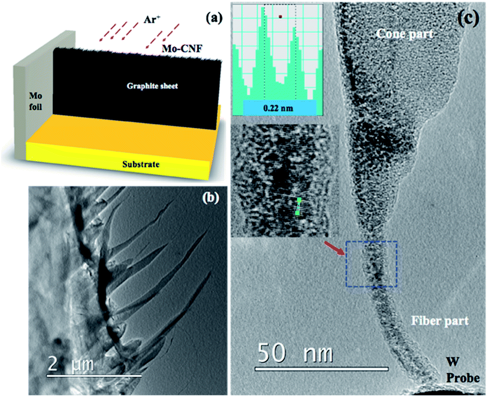 | ||
| Fig. 1 (a) Schematic diagrams showing the fabrication of amorphous Mo–CNF on the edge of graphite foil by the simultaneous bombardment of Ar+ on graphite and Mo foil. (b) A low-magnification TEM image showing vertically upstanding fibers on the edge of graphite foil. (c) A typical CNF with Mo embedded. The inset shows a Mo lattice with a lattice distance of 0.22 nm corresponding to the {110} plane. | ||
After a suitable CNF has been found, contact is established between the CNF and the W probe, as shown in Fig. 2(a). A bias voltage of 0–2.5 voltage is applied via the probe for 192 s, with the probe taken as the positive terminal and the fiber as the negative terminal. Fig. 2(a–h) are snapshots taken from Video S1† showing the agglomeration of the Mo particle and its movement due to electromigration. No visible transformation of CNF is observed until 126 s when agglomeration of Mo begins. A column of agglomerated Mo can be observed to be moving towards the tip of the fiber near the probe. The collection of Mo around the tip shows that electromigration is the dominant phenomenon, pushing Mo in the direction of the applied electric field. Around 130 s (Fig. 2(c)), it can be observed that smaller Mo particles are agglomerated into larger particles and the number of nanoparticles on the middle part of the CNF is reduced. An earlier agglomerated metallic column on the tip expands to a spherical shape around the CNF. From 140 s to 190 s, further agglomeration of Mo is observed around the tip with graphitization clearly observable around the middle of the CNF near the large agglomerated particle.
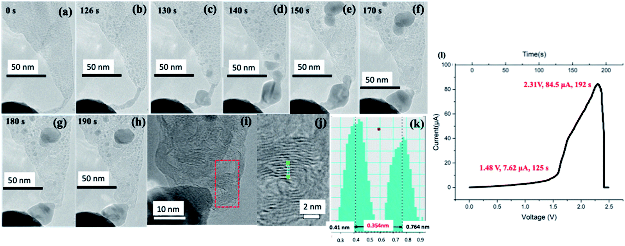 | ||
| Fig. 2 (a–h) Screenshots taken from Video S1† showing the transformation of Mo–CNF induced by the electromigration of Mo under the application of a bias voltage from 0 to 190 s. (i) A high-magnification image taken at the tip of the fiber near agglomerated metal showing the graphitic layer. (j) A high-magnification image taken around the red rectangular area of (i) showing multilayer graphene and a line profile taken across the layer showing the interlayer distance to be 0.34 nm (k). (l) An IV curve corresponding to (a–h) (Video S1†), showing the changes in the electrical properties of Mo–CNF during electromigration and graphitization. | ||
It is interesting to observe that the Mo bulk particle near the tip acts as a soldering agent connecting the probe and as-formed multilayer graphene. During the electromigration and graphitization process of CNF, a sudden change in IV curve is also observed. From the IV curve of Fig. 2(l), a steep increase in current can be observed around 125 s corresponding to the beginning of Mo electromigration at around 125 s (Fig. 2(b)) shown in Video S1.† Due to the conversion of amorphous CNF to multilayer graphene, conductivity is suddenly increased, leading to an increase in the value of the current. A very high current of 84.5 μA is flowing through the fiber. Fig. 2(i) shows a high-magnification TEM image near the tip of the remaining CNF attached to Mo, with the graphitic lattice clearly visible. As shown by the line profile (Fig. 2(k)) taken around the red rectangular selection of Fig. 2(i) shown in Fig. 2(j), the lattice distance is found to be around 0.35 nm, close to the reported value for graphene. Since the direction of Mo electromigration is from CNF towards to the probe, no significant presence of W was confirmed in the synthesized graphene using EDS, as shown in ESI S2.† To further demonstrate the electromigration and graphitization process, another set of experiments was carried out. As longer CNFs are unstable and may break during Joule heating, a constant bias is applied. Fig. 3(a–d), (e–g), (h–j) and (k–m) show the electromigration of Mo and the graphitization of CNF in 4 different steps. During the 1st step, triangular-shaped Mo crystal starts to agglomerate near the probe. With a continuous supply of voltage, a triangular crystal starts to grow (Fig. 3(c)) and a hexagonal-shaped crystal starts to grow, as shown in Fig. 3(d). In the 2nd step, we observe the further electromigration of Mo, and crystals near the probe merge to form a round shape, as shown in Fig. 3(e–g). During the 3rd step (Fig. 3(h–j)), further electromigration leads to the middle part of CNF being partially metal free with graphitization. The 4th step (Fig. 3(k–m)) shows complete graphitization of the CNF and its breakage. Fig. 4(a) shows graphitized CNF being completely separated from the agglomerated Mo particle attached to the probe. Fig. 4(b and c) shows a high-magnification TEM image taken near the tip of the broken CNF. It can be observed that, 5–10 layers of bamboo-like CNT are formed. Hollow structures are visible in the middle due to electromigration and evaporation of the Mo particle. Core-shell-like graphitic structures remained after evaporation of Mo particles, resembling graphitic foam. Graphitization happens around the Mo particle and its sudden evaporation leads to a bamboo-like carbon nanotube structure. Fig. 4(d and e) shows the upper areas 3 and 4 indicated in Fig. 4(a). The earlier CNF is found to be completely graphitized with the graphene lattice clearly visible and with amorphous carbon present. Earlier smaller Mo particles are completely agglomerated to a size of around 10 nm, as shown in Fig. 4(f). It should be noted that the tip of the CNF with its small diameter is converted to bamboo-like CNT structures whereas base of the CNF with a large area is converted to multilayered graphene. From these observations, it can be clearly stated that Mo acts as an efficient catalyst, leading to the graphitization of amorphous carbon. And agglomerated Mo are collected at the edge of the fiber.
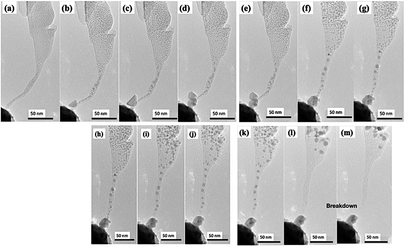 | ||
| Fig. 3 (a–m) Screenshots taken from an in situ TEM video (Video S2†), showing the gradual formation of a metallic crystal near the tip of the probe followed by the graphitization of the fiber. | ||
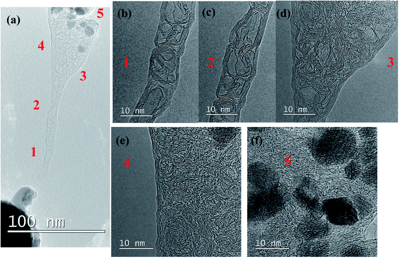 | ||
| Fig. 4 (a) A graphitized CNF separated from the Mo particle (b and c) A bamboo-like carbon nanotube with 3–8 layers observed near positions (1) and (2) of (a). (d–f) Figures showing porous graphitized structures on the cone part of the fiber near positions (3), (4) and (5) of (a). | ||
Conclusions
In conclusion, we demonstrated the rarely explored catalytic properties of Mo via in situ TEM studies. It was found that high-quality graphene can be synthesized using Mo as a catalyst. It was found that Joule heating induced electromigration in Mo–CNF serves the double purpose of the graphitization of CNF and the controllable agglomeration of Mo near the probe, acting as a soldering agent. This work can serve as a starting point for further research into Mo-based single-step graphene synthesis and nano-soldering.Experimental section
CNFs were grown on the edges of a graphite foil (2 cm × 5 cm). Mo foil of 25 μm thickness was used as the Mo source. Graphite foil and Mo foil were kept perpendicular to each other, as shown in schematic Fig. 1(a). Ar+ was bombarded simultaneously onto the edge of graphite and Mo foil using a Kaufmann-type ion gun (Iontech. Inc. Ltd, model 3-1500-100FC). During Ar+ bombardment, Mo and C are ejected and re-deposited on the edge of the graphite foil, leading to the formation of Mo-embedded CNF (Mo–CNF).Conflicts of interest
There are no conflicts to declare.References
- K. S. Novoselov, A. K. Geim, S. V. Morozov, D. Jiang, Y. Zhang, S. V. Dubonos, I. V. Grigorieva and A. A. Firsov, Science, 2004, 306, 666–669 CrossRef CAS
.
- A. C. Neto, F. Guinea, N. M. Peres, K. S. Novoselov and A. K. Geim, Rev. Mod. Phys., 2009, 81, 109 CrossRef
- A. A. Balandin, S. Ghosh, W. Bao, I. Calizo, D. Teweldebrhan, F. Miao and C. N. Lau, Nano Lett., 2008, 8, 902–907 CrossRef CAS
- K. I. Bolotin, K. J. Sikes, Z. Jiang, M. Klima, G. Fudenberg, J. Hone, P. Kim and H. L. Stormer, Solid State Commun., 2008, 146, 351–355 CrossRef CAS
- X. Li, W. Cai, J. An, S. Kim, J. Nah, D. Yang, R. Piner, A. Velamakanni, I. Jung and E. Tutuc, Science, 2009, 324, 1312–1314 CrossRef CAS
- S. Bae, H. Kim, Y. Lee, X. Xu, J.-S. Park, Y. Zheng, J. Balakrishnan, T. Lei, H. R. Kim and Y. I. Song, Nat. Nanotechnol., 2010, 5, 574 CrossRef CAS
- S. Sharma, G. Kalita, R. Hirano, S. M. Shinde, R. Papon, H. Ohtani and M. Tanemura, Carbon, 2014, 72, 66–73 CrossRef CAS
- X. Li, W. Cai, L. Colombo and R. S. Ruoff, Nano Lett., 2009, 9, 4268–4272 CrossRef CAS
- K. S. Kim, Y. Zhao, H. Jang, S. Y. Lee, J. M. Kim, K. S. Kim, J.-H. Ahn, P. Kim, J.-Y. Choi and B. H. Hong, Nature, 2009, 457, 706 CrossRef CAS
- L. Gao, W. Ren, H. Xu, L. Jin, Z. Wang, T. Ma, L.-P. Ma, Z. Zhang, Q. Fu and L.-M. Peng, Nat. Commun., 2012, 3, 699 CrossRef
- M. Zhang, K. Takei, B. Hsia, H. Fang, X. Zhang, N. Ferralis, H. Ko, Y.-L. Chueh, Y. Zhang and R. Maboudian, Appl. Phys. Lett., 2010, 96, 063110 CrossRef
- S. Naghdi, I. Jevremović, V. Mišković-Stanković and K. Y. Rhee, Corros. Sci., 2016, 113, 116–125 CrossRef CAS
- Y. Wu, G. Yu, H. Wang, B. Wang, Z. Chen, Y. Zhang, X. Shi, X. Xie, Z. Jin and X. Liu, Carbon, 2012, 50, 5226–5231 CrossRef CAS
- C. S. Hau-Riege and C. V. Thompson, Appl. Phys. Lett., 2001, 78, 3451–3453 CrossRef CAS
- A. Barreiro, F. Börrnert, S.-M. Avdoshenko, B. Rellinghaus, G. Cuniberti, M.-H. Rümmeli and L. M. K. Vandersypen, Sci. Rep., 2013, 3, 1115 CrossRef
- M. S. Rosmi, M. Z. Yusop, G. Kalita, Y. Yaakob, C. Takahashi and M. Tanemura, Sci. Rep., 2014, 4, 7563 CrossRef CAS
- J.-Y. Huang, F. Ding, B.-I. Yakobson, P. Lu, L. Qi and J. Li, Proc. Natl. Acad. Sci. U. S. A., 2009, 106(25), 0103–10108 CrossRef
- S. Sharma, M. S. Rosmi, Y. Yaakob, M. Z. M. Yusop, G. Kalita, M. Kitazawa and M. Tanemura, Carbon, 2018, 132, 165–171 CrossRef CAS
- M. Z. M. Yusop, P. Ghosh, Y. Yaakob, G. Kalita, M. Sasase, Y. Hayashi and M. Tanemura, ACS Nano, 2012, 6, 9567–9573 CrossRef CAS
- M. S. Rosmi, Y. Yaakob, S. Sharma, M. Z. Yusop, G. Kalita and M. Tanemura, IEEE, 2016, 622–623 Search PubMed
Footnote |
| † Electronic supplementary information (ESI) available: In situ TEM Videos S1and S2 are available as supplementary information. See DOI: 10.1039/c9ra05936a |
| This journal is © The Royal Society of Chemistry 2019 |