Effect of single metal doping on the thermoelectric properties of SnTe
Masoud
Aminzare
a,
Yu-Chih
Tseng
b,
Anbalagan
Ramakrishnan
c,
Kuei-Hsien
Chen
 c and
Yurij
Mozharivskyj
 *a
*a
aDepartment of Chemistry and Chemical Biology, McMaster University, Hamilton, Canada. E-mail: mozhar@mcmaster.ca
bCANMET Materials, Natural Resources Canada, Hamilton, Canada
cInstitute of Atomic and Molecular Sciences, Academia Sinica, Taipei 10617, Taiwan
First published on 6th November 2018
Abstract
SnTe, a lead-free chalcogenide-based material, shows potential to achieve high thermoelectric performance. This report presents a comparative study of different metallic dopants in SnTe and their effect on its microstructures, and mechanical and thermoelectric properties. Doped SnTe (Sn1−xAxTe, A = Co, Ni, Zn, Ge, and x = 0.01, 0.03, 0.05) materials are prepared by melting–quenching synthesis followed by spark plasma sintering. X-ray powder diffraction analysis showed that the solubility of Co, Ni, and Zn in the structure is in the range from 0 to 0.01; however, Ge can be doped in higher amounts. The back-scattered electron images and elemental maps revealed that the CoTe, Ni3SnTe2 and ZnTe impurity phases precipitate on the grain boundaries in the SnTe matrix. Ge-doped samples have more uniform microstructures with a very few Ge-rich regions, which implies higher Ge solubility in agreement with the XRD results. The existence of impurity phases in the Co-, Ni-, and Zn-doped samples yields lower lattice thermal conductivities without deterioration in charge transport properties, leading to higher ZT values relative to the pristine SnTe sample. The microhardness of the doped samples is also improved due to the crack growth suppression and crack branching.
Introduction
Owing to the growing global demands for energy efficiency and conservation, green, safe and reliable energy conversion technologies are becoming highly desirable. Thermoelectric (TE) materials are of particular interest as they can scavenge waste heat and turn it into electric current by using the Seebeck effect. Promising TE materials display a high Seebeck coefficient, S, high electrical conductivity, σ, and low thermal conductivity, k, whose values determine the dimensionless figure-of-merit ZT = S2σT/k at a given temperature T.1–3Lead chalcogenide (PbQ, Q = S, Se, and Te) compounds are among the promising thermoelectric materials as they exhibit high thermoelectric performance at mid-temperature ranges (600–900 K), and for this reason, they have long been studied for power generation applications.4–7 For instance, recent studies on lead chalcogenides yielded ZT ∼ 2.0 by applying band engineering and microstructure control.5,8–10 However, new regulations for environmentally hazardous substances aim to limit the use of lead, and adoption of lead chalcogenides for thermoelectric power generators does not seem viable. For these reasons, lead-free TE materials such as tin chalcogenides (SnQ) have attracted significant attention. Zhao et al. has recently reported a very high ZT of 2.6 at 900 K for SnSe single crystals.11 However, poor mechanical properties and the anisotropic nature of SnSe single crystals annihilate the feasibility of using them in real devices. On the other hand, thermoelectric properties of polycrystalline SnSe are not as exciting as those of its single crystalline analog.12,13 Meanwhile, tin telluride (SnTe), another member of tin chalcogenides, has physico-chemical properties very similar to PbTe: the same rock salt structure, narrow band gap, and similar band structure. Therefore, one can assume that TE properties of SnTe can be improved by using similar techniques applied to PbTe, such as the resonant level effect, band engineering, and nanostructuring.14–16
However, SnTe has its shortcomings; due to the intrinsic Sn vacancies, it possesses an ultrahigh hole density (>1021 cm−3), leading to a poor Seebeck coefficient, a high thermal conductivity, and thus relatively low ZT values. Several studies have been conducted to suppress the hole concentration to an appropriate level of ca. 1019 cm−3 through doping with elements that are efficient electron donors into lead chalcogenides, such as Sb and Bi.17,18 However, the outcomes were not satisfactory. Instead, it has been reported that Sn self-compensation (i.e. extra Sn) can successfully decrease the Sn vacancies and bring down the hole carrier concentration, leading to a 50% enhancement in the ZT value for the Sn1.03Te sample.15 While Sn self-compensation does reduce the hole concentration in SnTe, the resulting hole density is still relatively high and needs further optimization to achieve appropriate TE performance.
A desirable band gap for a good thermoelectric material operating at around 800 K is at least ∼0.3 eV (or 6–10 kBT, where kB is the Boltzmann constant and T is the operating temperature) according to theoretical studies, but it can also be larger depending on the specific mechanism of electron scattering.19 SnTe has band gaps (Eg) of ∼0.18 and ∼0.27 eV at room temperature and higher temperatures, respectively, which are smaller than the optimum values.15,19,20 The small band gap of SnTe (smaller than that of PbTe) causes bipolar effects at high temperatures. Furthermore, the energy separation between the light-hole and heavy-hole valence bands (ΔE(VB)L−Σ) is about 0.3–0.4 eV at 300 K, which is larger than that in PbTe.21,22 Because of the large ΔE(VB)L−Σ, heavy holes in the valence band do not contribute to charge transport and SnTe has a low S. Therefore, optimization of the electronic band structure of SnTe through band engineering is needed, if SnTe were to be used at high temperatures. By using appropriate dopant elements, one can simultaneously increase the band gap and reduce the energy difference between the light-hole and heavy-hole bands. Tan et al.15 demonstrated valence band engineering via isoelectronic doping of Sn with Cd. The Cd presence affects the electronic band structure through convergence of the light-hole and heavy-hole valence bands, leading to a larger Seebeck coefficient.15,23 In addition, Cd doping yields a larger band gap and better thermoelectric performance at high temperatures, as bipolar diffusion is minimized.15,23 As a result, a ZT value of ∼0.96 was achieved at 823 K for the p-type SnCd0.03Te sample, a 60% improvement over the undoped sample.15 Moreover, SnCd0.03Te with endotaxial CdS and ZnS nanoprecipitates displayed reduced lattice thermal conductivity while the power factor was preserved. The maximum ZTs of ∼1.3 and ∼1.1 were achieved at 873 K for CdS and ZnS-added specimens, respectively.15 Similar effects on the electronic band structure of SnTe were observed in Mg-, Mn-, Ca-doped samples.14,24–27
To further investigate the TE properties of doped SnTe, we explored new cation-doped SnTe samples. To the best of our knowledge, very few systematic studies have been conducted on the TE properties of Co-, Ni-, Zn-, and Ge-doped SnTe phases.
Experimental
Co (99.999 wt%), Ni (99.995 wt%), Zn (99.995 wt%), Ge (99.995 wt%), Sn (99.995 wt%), and tellurium (99.999 wt%) pieces were used for the synthesis without further purification. Initially, high quality polycrystalline ingots of Sn1−xAxTe (x = 0–0.05) were prepared through melting stoichiometric amounts of the starting elements in vacuum-sealed silica tubes (10−3 Torr, 10 mm in diameter). The samples were slowly heated to 1000 °C over 10 h, soaked for 6 h, and then rapidly quenched in an ice-water mixture. The ingots were hand ground in an agate mortar, and the powders were densified by spark plasma sintering (SPS) at 600 °C with a uniaxial pressure of ∼50 MPa for 5 minutes. The density of all SPS samples was determined using Archimedes' method, which gave values ≥96% of the theoretical density. In order to measure thermoelectric properties, the SPS samples were cut into thin square plates (∼10 × 10 × 1 mm3) and bars (2 × 2 × 10 mm3) with a low-speed saw.X-ray diffraction (XRD) and energy dispersive spectroscopy (EDX) were employed to characterise the samples' crystallinity, homogeneity, chemical composition and elemental distributions. Powder XRD data were collected for 2θ = 20–140° on a PANalytical X'Pert Pro diffractometer with a linear X'Celerator detector and Cu-Kα1 (λ = 1.5406 Å) radiation at room temperature. Sample powders were deposited on a zero-background silicon disc. The XRD data were refined by the Rietveld method using the Rietica program.28 Microstructural analyses were performed using scanning electron microscopy (SEM, Tescan Vega II LSU, USA) in both secondary and backscattered modes of imaging. The samples were prepared by hand polishing using 2400 SiC and 4000 SiC polishing papers.
Electrical conductivity and Seebeck coefficients were measured simultaneously under a He atmosphere from room temperature to 600 °C on a ULVAC-RIKO ZEM-3 instrument system. Pure SnTe, as the reference sample, was measured on two different ZEM-3 instruments in two different places, and the average value is taken. Surfaces of each specimen were gently polished using 2400 SiC and 4000 SiC papers before measurements.
The thermal diffusivity, D, was directly measured from room temperature to 600 °C by using the laser flash diffusivity method on a Netzsch LFA-457 instrument. Square samples with the dimensions of ∼10 × 10 mm and ∼1 mm thickness were used for the measurements. The temperature-dependent heat capacity, Cp, was derived using a standard sample (pyroceram) in a LFA-457. The total thermal conductivity, κtotal, was calculated using the formula κtotal = DCpρ, where ρ is the density.
Vickers microhardness was measured on the 5% doped samples using a diamond indenter on a commercial Zwick Roell ZHU 2.5 instrument, where the force applied was 2 N and the indent was kept for 10 s. The equation HV = 1.854 × L/(2d)2 was used to determine the Vickers hardness values (kgf mm−2), with L being the indentation load and 2d the diagonal length of the indentation. The uncertainty of the microhardness results is about 5%.
Results and discussion
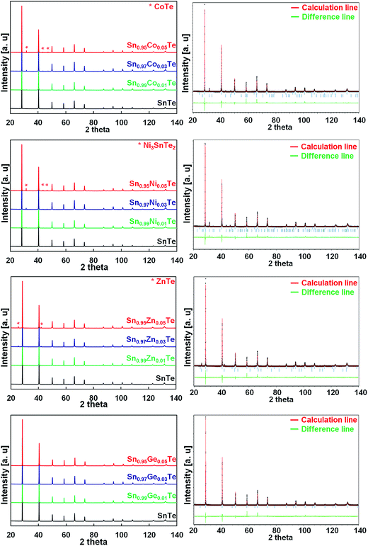
Fig. 1 shows the powder XRD patterns of the Co, Ni, Zn, and Ge-doped Sn1−xAxTe bulk samples after SPS along with the Rietveld refinement results for the 5% doped samples. The main Bragg reflections for all the samples fit the face centered cubic (fcc) structure of SnTe (space group Fm![[3 with combining macron]](https://www.rsc.org/images/entities/char_0033_0304.gif) m). The 1% doped samples are pure within the X-ray detection limits. Rietveld refinements show an excellent agreement between the experimental spectra and the theoretical patterns generated. When the dopant fractions are above 1%, secondary phases can be clearly observed. The amount of impurities calculated from the Rietveld refinement is summarized in Table 1. When dopant elements are introduced on the Sn-site, the lattice parameters are expected to decrease since the cationic radii of the dopants are smaller than that of Sn2+ (Ge2+ 0.65 Å29,30 < Co2+ 0.70 Å ≅ Ni2+ 0.70 Å < Zn2+ 0.74 Å < Sn2+ 0.93 Å).31 Indeed, there is a slight peak shift towards higher 2θ for Co-, Ni-, Zn- and Ge-doped samples, which proves successful substitutions on the Sn site (Table 1).
m). The 1% doped samples are pure within the X-ray detection limits. Rietveld refinements show an excellent agreement between the experimental spectra and the theoretical patterns generated. When the dopant fractions are above 1%, secondary phases can be clearly observed. The amount of impurities calculated from the Rietveld refinement is summarized in Table 1. When dopant elements are introduced on the Sn-site, the lattice parameters are expected to decrease since the cationic radii of the dopants are smaller than that of Sn2+ (Ge2+ 0.65 Å29,30 < Co2+ 0.70 Å ≅ Ni2+ 0.70 Å < Zn2+ 0.74 Å < Sn2+ 0.93 Å).31 Indeed, there is a slight peak shift towards higher 2θ for Co-, Ni-, Zn- and Ge-doped samples, which proves successful substitutions on the Sn site (Table 1).
| Sample | SnTe | Co-doped | Ni-doped | Zn-doped | Ge-doped | ||||||||
|---|---|---|---|---|---|---|---|---|---|---|---|---|---|
| 1% | 3% | 5% | 1% | 3% | 5% | 1% | 3% | 5% | 1% | 3% | 5% | ||
| a A very small impurity peak is observed at 2θ ≅ 27.3. It can be attributed to elemental Ge. | |||||||||||||
| a, Å | 6.3234(1) | 6.3198(1) | 6.3202(1) | 6.3211(1) | 6.3164(1) | 6.3140(1) | 6.3151(1) | 6.3222(1) | 6.3212(1) | 6.3217(1) | 6.3186(1) | 6.3117(1) | 6.3047(1) |
| Impurity wt% | 0 | 0.23(2) | 0.80(2) | 1.36(2) | 0.34(4) | 1.08(3) | 1.88(4) | 0.47(5) | 1.35(3) | 2.36(4) | 0 | 0 | <0.1a |
The 3 and 5% Co-, Ni-, and Zn-doped samples contain CoTe, Ni3SnTe2, and ZnTe impurities, respectively, and their fraction increases with the doping level (Table 1). The lattice parameters combined with the phase analysis suggest that the solubility limit for Co and Ni is about 1%. For the Zn case, the lattice parameters are not a reliable guide; however the phase analysis suggests similar solubility. For the Ge substitution, the lattice parameter decreases gradually till 5 at% of Ge and nearly no impurities are detected (Table 1).
It has been demonstrated that different elements have different solubility behaviours in SnTe; however, the solubility limits for Co, Ni and Zn are much lower than those observed for other dopants.14,24,25,32 Wu et al.25 reported up to 13% solubility of Mn in SnTe (on the Sn site). The authors observed that the (200) peak shifts to larger angles up to 13% of Mn and then to lower angles for higher Mn concentrations (Mn2+ radius is 0.66 Å and that of Sn2+ is 0.93 Å). Banik et al.33 observed a similar effect in the Sb-doped SnTe, where an increase in the Sb concentration up to x = 0.12 in Sn1−xSbxTe resulted in smaller lattice parameters. However, past x = 0.12, the lattice parameters of Sn1−xSbxTe started to increase, and this was accompanied by formation of SnmSb2nTe3n+m intergrowth nanostructures in the SnTe matrix.33 In the current work, a similar lattice behaviour is observed in the Co-, Ni-, and Zn-doped samples.
Scanning electron microscope (SEM) and backscattered electron (BSE) images (Fig. 2–5) were taken for 5% doped samples. Significant differences between the bright and dark contrast were observed in the Co, Ni, and Zn-doped specimens. The Co-, Ni-, and Zn-containing impurities precipitate primarily on the grain boundaries; additionally, the impurities display different precipitation patterns at the grain boundaries. The presence of secondary phases agrees with the XRD results that showed two phases for doping levels above 1%. The secondary electron (SE) and backscattered electron (BSE) images for the Ge-doped sample are different from those with other dopants. The distribution of Ge is almost homogeneous on the microscale, showing very few regions rich in Ge. When the Ge amount is below 5%, the samples can be assumed as a single phase, in agreement with the XRD results. The formation of impurities can have beneficial effects on the lattice thermal conductivity, and this relationship is discussed below.
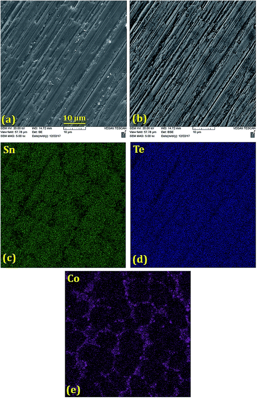 | ||
| Fig. 2 (a) Secondary electron image, (b) back-scattered electron image and (c–e) elemental mappings of Sn, Te and Co in the polished Sn0.95Co0.05Te sample prepared via SPS. Co-richer precipitates are found on the grain boundaries with an average grain size of ∼10 μm. The lack of Sn on the grain boundaries and uniform Te distribution confirm formation of CoTe on the grain boundaries, in agreement with the XRD results (Fig. 1(a) and (b)). | ||
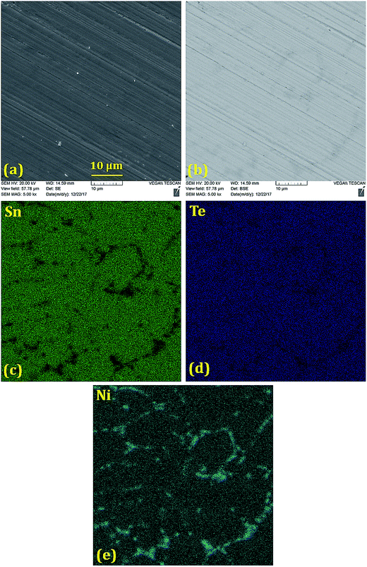 | ||
| Fig. 3 (a) Secondary electron image, (b) back-scattered electron image and (c–e) elemental mappings of Sn, Te and Ni in the polished Sn0.95Ni0.05Te sample prepared via SPS. A Ni-richer phase precipitates on the grain boundaries and within the grains with an average grain size ≤10 μm. A significant reduction in the Sn signal and slight reduction in the Te signal on the grain boundaries are consistent with the formation of Ni3SnTe2 as identified in the XRD patterns (Fig. 1(g) and (h)). | ||
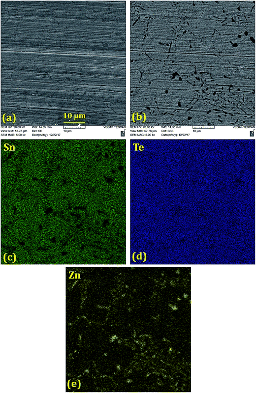 | ||
| Fig. 4 (a) Secondary electron image, (b) back-scattered electron image and (c–e) elemental mappings of Sn, Te and Zn in the polished Sn0.95Zn0.05Te sample prepared via SPS. Sn is absent in the Zn-rich areas, while the Te distribution is uniform throughout the sample. The elemental mapping supports formation of the ZnTe impurity, as witnessed in the XRD patterns (Fig. 1(c) and (d)). | ||
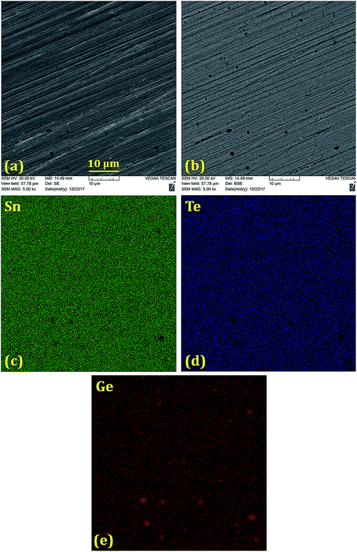 | ||
| Fig. 5 (a) Secondary electron image, (b) back-scattered electron image and (c–e) elemental mappings of Sn, Te and Ge in the polished Sn0.95Ge0.05Te sample prepared via SPS. The Ge distribution is almost uniform with very few Ge-rich regions smaller than 1 μm. Sn and Te are deficient in the Ge-rich regions. The Ge-rich regions are not detected in the XRD patterns due to their small size and numbers (Fig. 1(e) and (f)). | ||
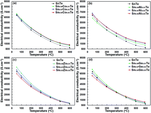
Fig. 6 shows the temperature-dependent electrical conductivity σ(T) of the Sn1−xAxTe sample. The σ(T) of the all samples decreases with increasing temperature, which is representative of heavily doped semiconductors. Overall, the electrical conductivities of Sn1−xAxTe samples reach 7130–1130 S cm−1, 7300–1220 S cm−1, 7710–870 S cm−1, and 7270–860 S cm−1 for the Co-, Ni-, Zn-, and Ge-doped samples, respectively, within the measured temperature range. For all dopants, the electrical conductivity of the 1%-doped samples is higher than that of SnTe, which is likely due to a higher carrier density. For the Zn- and Ge-containing samples, the conductivity generally decreases for the dopant concentrations above 1%. For the Ni-doped samples, electrical conductivity rises slightly as the Ni amount increases from 1% to 3% (Fig. 6(b)). This can be attributed to the formation of the Ni3SnTe2 impurity, which reduces the overall Sn/Te ratio and thus increases the charge carrier concentration of the SnTe matrix. With increasing temperature, the electrical conductivity of the 1, 3 and 5% doped samples converges.
If we treat the dopant substitutions on the Sn site as an isovalent one, the carrier concentration should remain unchanged upon doping. In general, this is true as the electrical conductivity of all doped samples is relatively close to that of the pristine one (Fig. 6). However, almost all 1% doped samples have a slightly higher electrical conductivity compared to the pristine sample suggesting an increased number of charge carriers. This observation is in agreement with the literature results, which indicate that Sn vacancies can be induced by limited doping on the Sn site, leading to an increase in the hole concentration.31 Doping above 1% in our samples does not change the charge carrier concentration but instead introduces more impurities/defects, leading to lower carrier mobility and conductivity. Similar effects were reported for Ag-doped SnTe specimens, where electrical conductivity decreased because of the increased charge carrier scattering by Ag-doping in the SnTe matrix.31
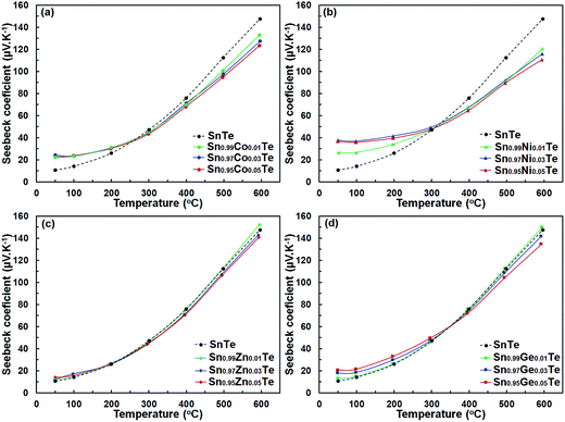
The Seebeck coefficient, S, for all Sn1−xAxTe samples is positive (Fig. 7), indicating p-type conductivity. Changes in the S of the doped samples are in general agreement with changes in σ(T); i.e. a larger charge carrier concentration yields a higher conductivity but a lower thermopower. Additionally, for a given dopant, the Seebeck coefficient and its temperature behaviour are similar for different dopant levels. Interestingly, the room temperature Seebeck coefficients of the Co- and Ni-doped samples are visibly higher than that for the pristine sample despite their higher electrical conductivity, which is contradictory to the typical behavior expected for a degenerate semiconductor. Additionally, the thermopower of the Co- and Ni-doped samples becomes lower at higher temperatures. A similar behaviour was observed in the Sn1+xTe samples and is attributed to the position of the Fermi level.15,34 In pure SnTe with a large hole concentration, the Fermi level is lower in energy and closer to the heavy-hole band than that in the less conductive, compensated Sn1+xTe samples with x > 0. This yields a larger thermopower for SnTe at room-temperature. As the temperature increases, carriers from the heavy band in the compensated Sn1+xTe samples become excited and their Seebeck coefficients increase faster than that of SnTe.35,36 The heavy-hole band contribution to the high temperature properties of Sn1+xTe was confirmed by Tan et al.15 through temperature-dependent Hall measurements. The charge transport properties of the Co- and Ni-doped samples can be explained in a similar fashion; since these samples are more electron deficient (i.e. have more holes) than pure SnTe, their Fermi levels are closer to the heavy-hole band and their room-temperature thermopower is higher.
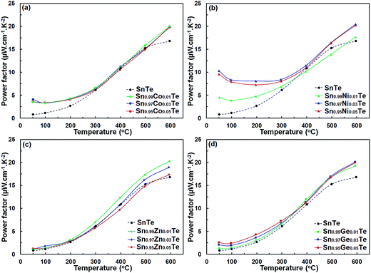
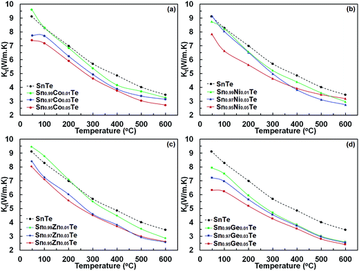
Power factors for the pristine and doped samples are depicted in Fig. 8. The pure SnTe has a power factor of ∼17 μW cm−1 K−2 at 300 °C, which is in good agreement with the literature data.14,24,32,33 Overall, power factors of doped samples (Sn1−xAxTe) are higher than that of the pristine one, mainly due to their higher electrical conductivity. Thermal conductivities of the Sn1−xAxTe samples are presented in Fig. 9. All thermal conductivities decrease with increasing temperature and doping concentrations. Thermal conductivity includes electronic thermal conductivity κe and lattice thermal conductivity κlat; κt = κe + κlat. The electronic part, κe, can be estimated from the Wiedemann–Franz law (κe = LσT), where L, σ, and T are the Lorenz number, electrical conductivity, and absolute temperature, respectively. The Lorenz number at a given temperature can be approximated from the experimental Seebeck coefficient according to37
 | (1) |
Table 2 summarizes the calculated Lorenz number, and electronic and lattice thermal conductivities for the pristine and 5% doped samples at 50 and 600 °C. It has to be mentioned that the Lorenz number for PbTe evaluated in this way is accurate within 20% for PbTe due to the presence of non-parabolic bands.37 Since the band structure of SnTe is similar to that of PbTe, a similar uncertainty for the Lorenz number is expected for our samples.
| Sample | Temperature (°C) | κ t (W m−1 K−1) | L (× 10−8 W Ω K−2) | κ e (W m−1 K−1) | κ lat (W m−1 K−1) |
|---|---|---|---|---|---|
| Pristine | 50 | 9.12 | 2.41 | 5.34 | 3.78 |
| 600 | 3.47 | 1.78 | 1.20 | 2.26 | |
| 5% Co | 50 | 7.40 | 2.32 | 5.35 | 2.05 |
| 600 | 2.72 | 1.84 | 2.09 | 0.63 | |
| 5% Ni | 50 | 7.84 | 2.23 | 5.11 | 2.73 |
| 600 | 3.20 | 1.88 | 2.71 | 0.49 | |
| 5% Zn | 50 | 8.04 | 2.39 | 4.98 | 3.05 |
| 600 | 2.62 | 1.80 | 1.37 | 1.25 | |
| 5% Ge | 50 | 6.33 | 2.34 | 4.57 | 1.76 |
| 600 | 2.41 | 1.81 | 1.74 | 0.67 |
Electrical conductivities of the doped samples are close to that of the undoped one, and their electronic thermal conductivities at given temperatures are almost identical. However, the lattice thermal conductivities of the Sn1−xAxTe samples are lower than that of the undoped one. This decrease can be associated with the higher phonon scattering due to the higher impurity concentrations upon doping. The thermal conductivity values are similar to those in the literature.14,24,32,33 The order of the lattice thermal conductivities of Sn1−xAxTe at room temperature is pristine > Zn-doped > Ni-doped > Co-doped > Ge-doped samples. It is worth mentioning that the Ge-doped sample is very homogeneous, but the Co-, Ni- and Zn-doped samples have significant intergrain impurity precipitates (Fig. 2–5). The sequence becomes pristine > Zn-doped > Ge-doped > Co-doped > Ni-doped samples at the highest temperature, indicating that precipitates on grain boundaries become more effective in scattering phonons at higher temperatures. Remarkably, the substitution of 5% Co, Ge, and Ni decreases the lattice thermal conductivity to the point where it is close to the amorphous limit at high temperature (κlat ∼0.4–0.5).21,38
As mentioned above, the difference in the thermal conductivity between the doped and pristine SnTe samples can be rationalized in terms of the microstructure. Generally, the thermal conductivity is highly sensitive to precipitates at grain boundaries, whereas the electrical conductivity and Seebeck coefficient are less. The 5% Co-, Ni- and Zn-doped samples have slightly different lattice thermal conductivities. This may stem from the different sizes of the CoTe, Ni3SnTe2, and ZnTe precipitates and their different distribution patterns. Similar reductions in lattice thermal conductivities have been reported for Ga-, Mn-, Ca-, and Cu-doped SnTe due to the strong phonon scattering produced by the formation of GaTe, MnTe, CaTe, and Cu2Te impurities, respectively.14,24,25,32,38 An analogous behaviour was also observed for CdS/ZnS secondary phases introduced into the SnTe samples. Tan et al.15 composited SnCd0.03Te with endotaxial CdS and ZnS nanoscale precipitates to reduce the lattice thermal conductivity without affecting the power factor. These nanostructures formed point defects via integrating Cd or Zn atoms into the matrix at high temperatures with a minimal influence on both the carrier mobility and the band gap of SnTe, thus enhancing the high temperature thermoelectric performance.
In comparison to the Co-, Ni- and Zn-doped samples, the Ge-doped ones appear to have a different mechanism for phonon scattering. Ge is nearly uniformly distributed within the matrix with very few Ge-rich regions smaller than 1 μm. Lee et al.31 found a significant reduction in klat due to Sn defects induced by doping, and the same might be happening in the Ge-doped samples here. There is also a possibility of formation of nanoclusters embedded in the structure, causing further lattice thermal conductivity reduction. However, the validity of this idea can only be verified with future TEM studies.
Fig. 10 illustrates lattice thermal conductivities of the Co-, Ni- and Ge-doped SnTe samples (results for the Zn-doped sample are not shown as it has a higher lattice thermal conductivity) in comparison with other singly doped SnTe compounds.14,15,17,24,25,38–42 It is apparent that the current dopants yield a significant reduction in the lattice thermal conductivity (0.6–0.5 W m−1 K−1 at 600 °C K) and bring it close to the amorphous limit of κlat (0.4–0.5).43 However, both electronic thermal conductivities and low-temperature lattice thermal conductivities are still high, and further reductions are necessary to optimize the TE performance of the Co-, Ni-, Zn- and Ge-doped SnTe samples.
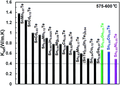 | ||
| Fig. 10 Comparison of the lattice thermal conductivity for different singly doped SnTe samples14,15,17,24,25,38–42 at 575–600 °C. The lattice thermal conductivities of our Co-, Ni-, and Ge-doped samples are comparable to the lowest κL values reported for SnTe so far. | ||
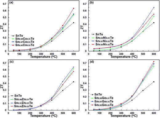
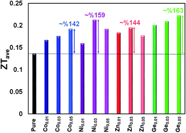
The ZT values as a function of temperature for the pristine and doped samples are presented in Fig. 11. The maximum ZT values of 0.63, 0.65, 0.64, and 0.72 are achieved for the Sn0.95Co0.05Te, Sn0.97Ni0.03Te, Sn0.97Zn0.03Te, and Sn0.95Ge0.05Te specimens at 600 °C, respectively. All doped samples show higher ZT values than the pure sample mostly due to decreases in their thermal conductivities. These results suggest that the current dopants can successfully improve the thermoelectric performance of SnTe. Moreover, Sn0.95Co0.05Te, Sn0.97Ni0.03Te, Sn0.97Zn0.03Te, and Sn0.95Ge0.05Te display 142, 159, 144, and 163% enhancements of the average figure of merit, ZTave (average of all ZT values from room temperature to 600 °C) in comparison with the pure SnTe (Fig. 12).
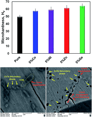
Mechanical properties are vital for thermoelectric applications as well. The material should be strong enough to withstand thermal cycling, thermal shock, machining, etc. in order to be used in large-scale device applications. The Vickers microhardness indentation method has been used to measure the mechanical properties of the pristine and 5% doped samples (Fig. 13). Overall, the rigidity of the doped materials is increased compared with that of the pure one. It is known that a pure SnTe material intrinsically contains Sn vacancies, which diminishes its mechanical strength. However, appropriate dopants, leading to fewer Sn vacancies, increase the rigidity of the material. This effect was observed in GeTe compounds, where Bi doping improved their mechanical properties through Ge vacancy reduction.44 Furthermore, crack growth suppression and crack branching are other two possible mechanisms contributing to the rigidity. Both can be induced by dopants, which reduce the energy of the cracks and stop the crack propagation inside the sample. Examples of crack growth suppression and crack branching are shown in Fig. 13. We believe that these two mechanisms are dominant in the Co-, Ni-, and Zn-doped samples, while reduction in the Sn vacancies can be instrumental in the Ge-doped one.
While doping increased the rigidity of our samples, our microhardness values are lower than some reported in the literature. This might be due to the large grain size of our samples (≥10 μm). In this respect, a smaller grain size in the range of nanometers together with secondary nanosize phases not only could enhance the mechanical properties but could also lower the thermal conductivity by increased phonon scattering.
Conclusion
As the lead-free rock-salt analogue of PbTe, SnTe can be used as a green thermoelectric material in real applications, if one can overcome its drawbacks such as a high hole concentration, low Seebeck coefficient, and high thermal conductivity through appropriate doping and nanostructuring. The current study suggests that 5% substitution of Co, Ni, and Ge decreases the high temperature lattice thermal conductivity to the point where it is close to the amorphous limit (κlat ∼0.4–0.5). This is one of the lowest lattice thermal conductivities reported for SnTe-based materials so far. Such a reduction in the lattice thermal conductivity can be rationalized in terms of doping-related defects and existence of secondary phases between the grains, which increase the phonon scattering and thus decrease the lattice thermal conductivity. While impurities can affect carrier mobility, the almost unchanged Seebeck coefficient and substantial reduction in the lattice thermal conductivity yield an enhancement in the ZTmax values for the doped samples. The lattice thermal conductivity is still high at lower temperatures and needs to be reduced if possible. Likewise, the Seebeck coefficient will have be optimized to improve the TE material efficiency. Potentially, this can be achieved by co-doping and nanostructuring. Furthermore, the microhardness of the doped samples can be further improved through enhanced crack growth suppression and crack branching.Conflicts of interest
There are no conflicts to declare.Acknowledgements
This work was supported by a Discovery Grant and a CREATE HEATER Grant from the Natural Sciences and Engineering Research Council of Canada.References
- L. Bell, Science, 2008, 321, 1457–1461 CrossRef CAS PubMed.
- F. DiSalvo, Science, 1999, 285, 703–706 CrossRef CAS PubMed.
- J. Heremans, M. Dresselhaus, L. Bell and D. Morelli, Nat. Nanotechnol., 2013, 8, 471–473 CrossRef CAS PubMed.
- J. P. Heremans, V. Jovovic, E. S. Toberer, A. Saramat, K. Kurosaki, A. Charoenphakdee, S. Yamanaka and G. J. Snyder, Science, 2008, 321, 554–557 CrossRef CAS PubMed.
- Y. Z. Pei, X. Y. Shi, A. LaLonde, H. Wang, L. D. Chen and G. J. Snyder, Nature, 2011, 473, 66–69 CrossRef CAS PubMed.
- Q. Y. Zhang, H. Wang, W. S. Liu, H. Z. Wang, B. Yu, Q. Zhang, Z. T. Tian, G. Ni, S. Lee, K. Esfarjani, G. Chen and Z. F. Ren, Energy Environ. Sci., 2012, 5, 5246–5251 RSC.
- L. D. Zhao, S. H. Lo, J. Q. He, H. Li, K. Biswas, J. Androulakis, C. I. Wu, T. P. Hogan, D. Y. Chung, V. P. Dravid and M. G. Kanatzidis, J. Am. Chem. Soc., 2011, 133, 20476–20487 CrossRef CAS PubMed.
- K. Biswas, J. Q. He, Q. C. Zhang, G. Y. Wang, C. Uher, V. P. Dravid and M. G. Kanatzidis, Nat. Chem., 2011, 3, 160–166 CrossRef CAS PubMed.
- K. Biswas, J. Q. He, I. D. Blum, C. I. Wu, T. P. Hogan, D. N. Seidman, V. P. Dravid and M. G. Kanatzidis, Nature, 2012, 489, 414–418 CrossRef CAS PubMed.
- H. Wang, J. H. Bahk, C. Kang, J. Hwang, K. Kim, J. Kim, P. Burke, J. E. Bowers, A. C. Gossard, A. Shakouri and W. Kim, Proc. Natl. Acad. Sci. U. S. A., 2014, 111, 10949–10954 CrossRef CAS PubMed.
- L. D. Zhao, S. H. Lo, Y. S. Zhang, H. Sun, G. J. Tan, C. Uher, C. Wolverton, V. P. Dravid and M. G. Kanatzidis, Nature, 2014, 508, 373 CrossRef CAS PubMed.
- E. K. Chere, Q. Zhang, K. Dahal, F. Cao, J. Mao and Z. F. Ren, J. Mater. Chem. A, 2016, 4, 1848–1854 RSC.
- S. Sassi, C. Candolfi, J. B. Vaney, V. Ohorodniichuk, P. Masschelein, A. Dauscher and B. Lenoir, Appl. Phys. Lett., 2014, 104, 4 CrossRef.
- A. Banik, U. S. Shenoy, S. Anand, U. V. Waghmare and K. Biswas, Chem. Mater., 2015, 27, 581–587 CrossRef CAS.
- G. J. Tan, L. D. Zhao, F. Y. Shi, J. W. Doak, S. H. Lo, H. Sun, C. Wolverton, V. P. Dravid, C. Uher and M. G. Kanatzidis, J. Am. Chem. Soc., 2014, 136, 7006–7017 CrossRef CAS PubMed.
- G. J. Tan, F. Y. Shi, S. Q. Hao, H. Chi, L. D. Zhao, C. Uher, C. Wolverton, V. P. Dravid and M. G. Kanatzidis, J. Am. Chem. Soc., 2015, 137, 5100–5112 CrossRef CAS PubMed.
- Q. Zhang, B. L. Liao, Y. C. Lan, K. Lukas, W. S. Liu, K. Esfarjani, C. Opeil, D. Broido, G. Chen and Z. F. Ren, Proc. Natl. Acad. Sci. U. S. A., 2013, 110, 13261–13266 CrossRef CAS PubMed.
- E. I. Rogacheva, J. Phys. Chem. Solids, 2008, 69, 259–268 CrossRef CAS.
- J. O. Sofo and G. D. Mahan, Phys. Rev. B, 1994, 49, 4565–4570 CrossRef CAS.
- A. J. Strauss, I. Melngailis and J. O. Dimmock, Phys. Rev. Lett., 1966, 16, 1193–1196 CrossRef.
- R. Moshwan, L. Yang, J. Zou and Z. G. Chen, Adv. Funct. Mater., 2017, 27, 18 CrossRef.
- S. Li, X. F. Li, Z. F. Ren and Q. Zhang, J. Mater. Chem. A, 2018, 6, 2432–2448 RSC.
- J. He, J. T. Xu, G. Q. Liu, H. Z. Shao, X. J. Tan, Z. Liu, J. Q. Xu, H. C. Jiang and J. Jiang, RSC Adv., 2016, 6, 32189–32192 RSC.
- R. A. Al Orabi, N. A. Mechosky, J. Hwang, W. Kim, J. S. Rhyee, D. Wee and M. Fornari, Chem. Mater., 2016, 28, 376–384 CrossRef.
- H. J. Wu, C. Chang, D. Feng, Y. Xiao, X. Zhang, Y. L. Pei, L. Zheng, D. Wu, S. K. Gong, Y. Chen, J. Q. He, M. G. Kanatzidis and L. D. Zhao, Energy Environ. Sci., 2015, 8, 3298–3312 RSC.
- J. Tang, B. Gao, S. Lin, J. Li, Z. Chen, F. Xiong, W. Li, Y. Chen and Y. Pei, Adv. Funct. Mater., 2018, 28, 1803586 CrossRef.
- W. Li, L. Zheng, B. Ge, S. Lin, X. Zhang, Z. Chen, Y. Chang and Y. Pei, Adv. Mater., 2017, 29, 1605887 CrossRef PubMed.
- B. A. Hunter and C. J. Howard, Rietica, Australian Nuclear Science and Technology Organization, Menai, Australia, 2000 Search PubMed.
- B. Macalik, M. Siu-Li and S. Zazubovich, Radiat. Eff. Defects Solids, 1998, 147, 11–16 CrossRef.
- T. Tsuboi, Phys. B, 1994, 193, 92–96 CrossRef CAS.
- M. H. Lee, D. G. Byeon, J. S. Rhyee and B. Ryu, J. Mater. Chem. A, 2017, 5, 2235–2242 RSC.
- R. Orabi, J. Hwang, C. C. Lin, R. Gautier, B. Fontaine, W. Kim, J. S. Rhyee, D. Wee and M. Fornari, Chem. Mater., 2017, 29, 612–620 CrossRef.
- A. Banik, B. Vishal, S. Perumal, R. Datta and K. Biswas, Energy Environ. Sci., 2016, 9, 2011–2019 RSC.
- R. F. Brebrick and A. J. Strauss, Phys. Rev., 1963, 131, 104–110 CrossRef.
- P. B. Littlewood, B. Mihaila, R. K. Schulze, D. J. Safarik, J. E. Gubernatis, A. Bostwick, E. Rotenberg, C. P. Opeil, T. Durakiewicz, J. L. Smith and J. C. Lashley, Phys. Rev. Lett., 2010, 105, 4 CrossRef PubMed.
- C. M. Jaworski, M. D. Nielsen, H. Wang, S. N. Girard, W. Cai, W. D. Porter, M. G. Kanatzidis and J. P. Heremans, Phys. Rev. B, 2013, 87, 10 CrossRef.
- H. S. Kim, Z. M. Gibbs, Y. L. Tang, H. Wang and G. J. Snyder, APL Mater., 2015, 3, 5 Search PubMed.
- Y. Z. Pei, L. L. Zheng, W. Li, S. Q. Lin, Z. W. Chen, Y. Y. Wang, X. F. Xu, H. L. Yu, Y. Chen and B. H. Ge, Adv. Electron. Mater., 2016, 2, 8 Search PubMed.
- J. He, X. J. Tan, J. T. Xu, G. Q. Liu, H. Z. Shao, Y. J. Fu, X. Wang, Z. Liu, J. Q. Xu, H. C. Jiang and J. Jiang, J. Mater. Chem. A, 2015, 3, 19974–19979 RSC.
- G. J. Tan, W. G. Zeier, F. Y. Shi, P. L. Wang, G. J. Snyder, V. P. Dravid and M. G. Kanatzidis, Chem. Mater., 2015, 27, 7801–7811 CrossRef CAS.
- G. J. Tan, F. Y. Shi, S. Q. Hao, H. Chi, T. P. Bailey, L. D. Zhao, C. Uher, C. Wolverton, V. P. Dravid and M. G. Kanatzidis, J. Am. Chem. Soc., 2015, 137, 11507–11516 CrossRef CAS PubMed.
- Z. W. Zhou, J. Y. Yang, Q. H. Jiang, Y. B. Luo, D. Zhang, Y. Y. Ren, X. He and J. W. Xin, J. Mater. Chem. A, 2016, 4, 13171–13175 RSC.
- D. G. Cahill, S. K. Watson and R. O. Pohl, Phys. Rev. B, 1992, 46, 6131–6140 CrossRef CAS.
- S. Perumal, S. Roychowdhury and K. Biswas, Inorg. Chem. Front., 2016, 3, 125–132 RSC.
| This journal is © The Royal Society of Chemistry 2019 |

