Beyond band bending in the WO3/BiVO4 heterojunction: insight from DFT and experiment†
Carles
Ràfols i Bellés
 a,
Shababa
Selim
 b,
Nicholas M.
Harrison
a,
Ehsan A.
Ahmad
 *a and
Andreas
Kafizas
 *bc
*bc
aThomas Young Centre, The London Centre for the Theory and Simulation of Materials, Royal School of Mines, Imperial College London, South Kensington, London, SW7 2AZ, UK. E-mail: ehsan.ahmad08@imperial.ac.uk
bDepartment of Chemistry, Imperial College London, South Kensington, London, SW7 2AZ, UK. E-mail: a.kafizas@imperial.ac.uk
cThe Grantham Institute – Climate Change and Environment, Imperial College London, South Kensington, London, SW7 2AZ, UK
First published on 9th November 2018
Abstract
Heterojunction photocatalysts can significantly enhance the efficiency of photocatalytic water splitting. It is well known that the key to such improvements lies at the interfacial region where charge separation occurs. Understanding the origins of this interfacial enhancement can enable the design of better performing water splitting devices. Therefore, in this work, a novel theoretical–experimental approach is developed for the study of photocatalytic heterojunctions using the model system – WO3/BiVO4, where it has been shown that the quantum efficiency of water splitting can approach unity at certain wavelengths. Our photoelectrochemical measurements of this heterojunction show a significantly enhanced performance over its separate components when illuminated through the BiVO4 side but not the WO3 side. This is indicative of more efficient electron transfer (i.e. from BiVO4 to WO3) than hole transfer (i.e. from WO3 to BiVO4) across the junction. Our classical band bending model of this junction predicts noticeable interfacial barriers, but could not explain the reduced performance under back illumination. Our atomistic model was used to investigate the effect of interfacial reconstructions and chemical interactions on the electronic structure of the system. The model reveals a non-staggered valence band, in contrast to the staggered conduction band, due to strong hybridization of valence band orbitals in both materials across the interface. This non-staggered valence band does not provide an energetic driving force for charge separation for hole transfer (i.e. from WO3 to BiVO4 under back illumination). Hence, a significant improvement in performance is only observed under front illumination. This combined approach, using both experiment and theory, results in a more complete understanding of a heterojunction photocatalyst system and provides unique insight into the interfacial effects that arise when two semiconductor materials are brought together, going beyond traditional band bending models.
Introduction
Since the first demonstration of photocatalytic water splitting by Fujishima and Honda in 1972, great efforts have been devoted to the development of efficient materials for renewable hydrogen generation, which would constitute a crucial step towards a fossil-fuel-free future.1 Studies have shown that an ideal water splitting photocatalyst should possess: (i) a band gap of 2.0–2.3 eV, (ii) adequate overpotential at the conduction and valence band edges for water reduction and oxidation respectively, (iii) good chemical stability, (iv) good conductivity/long charge carrier diffusion lengths, (v) minimal electron–hole recombination and (vi) fast surface reaction kinetics.2 Although such a photocatalyst has yet to be discovered, many potential candidates have emerged along with new ways of improving their photocatalytic properties (e.g. nanostructuring, doping, surface co-catalysts etc.). In particular, metal oxides such as TiO2,3 ZnO,4 WO3,5 BiVO4,6 Cu2O7 and α-Fe2O3 (ref. 8) have drawn much attention due to their ease of synthesis, low cost and durability, facilitating scalable industrial fabrication. Nevertheless, the water splitting activity of metal oxides falls shy of the requirements for commercial viability. Recent studies have shown that the coupling of materials, and the formation of a heterojunction, can result in substantial improvements in activity.7,9–11 When a heterojunction is formed from semiconductors with complementary band gaps, a synergetic improvement in solar-to-hydrogen efficiency can be achieved, where theoretical efficiencies of up to ∼27% can be reached vs. ∼17% for a single material.12A heterojunction is the interface that is formed between two dissimilar semiconductors. The use of heterojunctions can provide some leeway from the requirements of an ideal water splitting photocatalyst outlined above, since one material in the heterojunction can make up for the flaws of the other. For example, a narrow band gap semiconductor with poor chemical stability can be coupled with a wide band gap semiconductor of high chemical stability (e.g. Cu2O/TiO2).7 Such a heterostructure would possess high corrosion resistance and utilize a greater portion of the solar spectrum. Nevertheless, care must be taken when engineering such heterostructures. Staggered gap (type II) junctions, i.e. those where the valence and conduction bands of one semiconductor are higher in energy than the valence and conduction bands of the other, are the most desirable as this has been shown to promote the spatial separation of electron–hole carriers in opposing directions, and thus inhibit electron–hole recombination.13
Various type II heterojunctions have been investigated for applications in water splitting. Examples include TiO2/WO3,8 TiO2/ZnO,14 α-Fe2O3/WO3,15 WO3/BiVO4,15 Cu2O/TiO2,16 SrTiO3/BiVO4 (ref. 17) and α-Fe2O3/BiVO4.15 This article focuses on the WO3/BiVO4 heterojunction, which combines the excellent electron transport properties and chemical stability of WO3 with the visible light activity of BiVO4.16,18 Recently, Pihosh et al. developed nanostructured WO3/BiVO4 photoanodes that achieved a photocurrent of 6.72 mA cm−2 under 1 sun irradiation – a value approaching the theoretical maximum of 7.6 mA cm−2 and the highest reported to date for this system.19 It should be noted that photoanodes made from BiVO4 or WO3 alone achieve substantially lower photocurrents (highest reported values at 1 sun irradiation and an applied potential of 1.23 VRHE; BiVO4 = 4.4 mA cm−2 and WO3 = 2.4 mA cm−2).20,21 Despite various reports, the outstanding photocatalytic activity of the WO3/BiVO4 junction has been solely attributed to the type II nature of this heterojunction, without any rigorous study of the interface.22–27
The origin of the characteristic charge separation in type II heterojunctions lies in the interfacial region between the two semiconductors. From a classical perspective, the heterojunction can be modelled electrostatically. When the two materials are brought together, both the valence and conduction bands bend due to Fermi level equilibration. A band bending analysis can provide insightful information on the interfacial region that traditional band diagrams ignore. Moreover, Density Functional Theory (DFT) can be used to model the atomic structure and density of states at the interface, which would otherwise be highly challenging to experimentally study. DFT analysis probes short range interactions between the two materials at the interface, which are ignored when using a purely classical model. DFT analysis can determine any changes in the density of states, charge density and orbital hybridisation at the interface.
In this article we will investigate the WO3/BiVO4 junction using a combined experimental and theoretical approach. We develop novel, transferable methodologies for studying the interfacial properties of heterojunctions, using both classical and atomistic models. This approach can provide a more complete understanding of the heterojunction interface, and how localized interfacial properties impact on charge carrier behaviour and photocatalytic activity.
Methodology
Experimental
Flat, polycrystalline WO3/BiVO4 heterojunction photoanodes were synthesized in a two-step process. A thin layer of WO3 was first grown on FTO glass using an aerosol-assisted chemical vapor deposition (AACVD) process. The BiVO4 layer was then deposited on top of the WO3 layer using a metal–organic deposition (MOD) process. The individual analogues of WO3 and BiVO4 were also grown in an analogous fashion for comparison.X-ray diffraction analysis showed that the WO3 and BiVO4, in both heterojunction and individual samples, were polycrystalline and adopted monoclinic structures (BiVO4 = I112/b; WO3 = P121/n1) (Fig. S1 & S2†). Top-down and side-on scanning electron microscopy (SEM) showed that all films were flat and dense (Fig. S3†); WO3 layers were ∼290 nm thick and BiVO4 layers were ∼340 nm thick. With knowledge of film thickness, UV-visible absorption spectroscopy was used to determine the absorption coefficients, band gap energies and penetration depths at supra-band gap light in both WO3 and BiVO4 (Fig. S4–S6†).
Computational
Calculations were performed using density functional theory methods using a linear combination of atomic orbitals (LCAO) basis set as implemented in CRYSTAL14 software where the atoms were described using basis sets reported in the literature (oxygen,28 tungsten,29 bismuth30 and vanadium31). The B3LYP hybrid functional was used to relax the individual BiVO4 and WO3 structures as well as the WO3/BiVO4 heterojunction, as it has shown to be reliable for a range of transition metal oxides.32–36 The tolerance for the truncation criteria of the bielectronic integrals appearing in the self-consistent field (SCF) was set to 10−8 for Coulomb overlap, 10−8 for Coulomb penetration 10−8 for exchange pseudo-overlap in the direct space and 10−16 for exchange pseudo-overlap in the reciprocal space. The condition for the SCF convergence was set to 10−7 au on the total energy difference between two subsequent cycles. The reciprocal space was sampled according to a regular sublattice with a shrinking factor (input IS) of 8.Surface energy calculations were carried out for the low index surfaces of WO3 to identify the crystallographic facet with the lowest surface energy, i.e., the most stable. Low energy facets are more likely to dominate the surface area of particles in polycrystalline samples and hence there is a higher likelihood of an epitaxial heterojunction with BiVO4 forming on the lowest energy WO3 surface if the lattices can align. This consideration ensures that the model studied in this work is more representative of experiment. A more detailed description of the interface modelling can be found in the ESI.†
Results
Water splitting activity was assessed using photoelectrochemical methods (Fig. 1). Incident photon to current efficiencies (IPCEs) were measured at: (i) a fixed applied potential of 1.23 VRHE for various wavelengths (250 to 550 nm) under front (Fig. 1a) and back (Fig. 1b) irradiation. Under front illumination, the WO3/BiVO4 heterojunction sample outperformed its individual analogues (Fig. 1a). In general, higher IPCEs were observed over the range of supra-band gap wavelengths measured, particularly in the near visible region. It was clear that there was synergy, as the WO3/BiVO4 junction possessed both the visible-light activity of the BiVO4 and high conversion efficiency of WO3.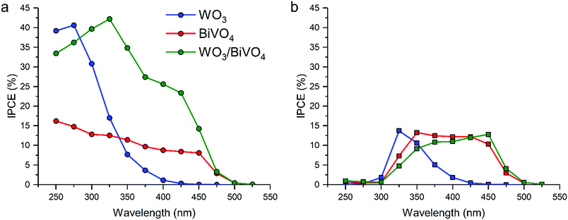 | ||
| Fig. 1 Incident photon to current efficiency (IPCE, %) vs. wavelength measured at 1.23 VRHE for front (a) and back (b) illumination in WO3, BiVO4 and the WO3/BiVO4 junction. | ||
Under back illumination, all samples showed low IPCEs from ≤325 nm, due to light absorption by the FTO substrate (Fig. 1b). Focusing on wavelengths ≥ 350 nm, the WO3/BiVO4 sample showed substantially lower IPCEs under back illumination compared with front illumination. It is also worth noting that, under back illumination, the WO3/BiVO4 junction displays a higher conversion efficiency at wavelengths where WO3 absorbs light less strongly (400–500 nm). This shows that the movement of holes in the WO3/BiVO4 junction, from WO3 across the WO3/BiVO4 junction and into the electrolyte, is less efficient compared with the parent materials, which results in a poorer performance in the WO3/BiVO4 junction under back illumination. We do not attribute this to poor hole transport in the BiVO4 layer, as the pure material shows improved IPCEs under back irradiation.
To further investigate the drop in performance of the WO3/BiVO4 heterojunction under back illumination, the light absorption behaviour, interfacial band bending and electronic structure of this junction are analysed.
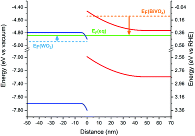
Using experimental methods, the band alignment of the WO3/BiVO4 heterojunction has been determined by several research groups using the flat band potential and optical bandgap of each individual material;25,27 however, to our knowledge, the band bending at the interface of this junction has not previously been determined. The band bending of the valence and conduction bands, upon Fermi level equilibration, was calculated (Fig. 3) using the average of typical values of the flat-band potential and donor densities from the literature (Table S1†). A summary of the parameters used can be found in Table S2.† The band bending diagram shows a rather asymmetric bending of the bands near the heterojunction interface. The energy difference between the bulk and interfacial region is approximately three times larger in BiVO4 (∼300 meV) than in WO3 (∼100 meV). In addition, the width of band bending is smaller in the WO3 layer (∼5 nm) compared with the BiVO4 layer (∼45 nm). The origin of this disparity arises from the difference in donor densities of the two materials. Typical donor densities in BiVO4 (∼1018 cm−3) are at least an order of magnitude lower than typical donor densities in WO3.26,27,37–39 Upon Fermi level equilibration, electrons in BiVO4 are transferred into the WO3 layer, as it possesses a lower Fermi level energy. This causes the Fermi level of WO3 to rise, but only marginally, since WO3 possesses a significantly higher donor density than BiVO4. On the other hand, this electron transfer, and disparity in donor density, causes the Fermi level in BiVO4 to decrease more substantially.
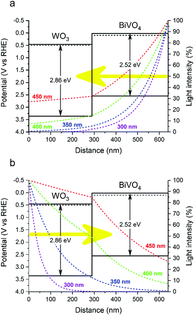 | ||
| Fig. 2 Band diagram and light absorption profiles across the WO3/BiVO4 heterojunction for 300, 350, 400 and 450 nm wavelengths under front (a) and back (b) illumination. | ||
This asymmetric band bending can have a severe impact on the performance of the heterojunction. In the absence of applied potential, electrons must overcome a ∼300 meV energy barrier to move from the BiVO4 layer into the WO3 layer. At room temperature, it is unlikely that this energy barrier will be surpassed by thermal promotion (kT ∼ 26 meV). In the reverse direction, holes must overcome a substantially smaller ∼100 meV barrier to move from the WO3 layer into the BiVO4 layer. However, band bending of the BiVO4 valence band will encourage holes to accumulate at the interface (and thus, will oppose their migration to the BiVO4/electrolyte interface). These energetic barriers can severely inhibit the photocatalytic function of the heterojunction at low applied potentials. However, in the presence of more substantial applied potentials, band bending at the WO3/BiVO4 interface will be less pronounced, and better facilitate charge separation across this type II junction. We postulate lower onset potentials can be achieved if the energetic barriers, caused by band bending, are minimized. This could be achieved by tuning the donor densities of one/both layers through doping40,41 or creating a doping gradient.42,43
The band bending, described in the previous section, was modelled classically using information acquired from the bulk materials, and ignores any structural changes that will likely occur when the interface is formed. Moreover, probing these structural changes using experimental methods is highly challenging. To overcome these limitations, the WO3/BiVO4 heterojunction was modelled using DFT methods. This allowed us to determine the interfacial bonding and structural changes that were likely, and how this impacted on the density of states & band alignment.
The calculated lattice parameters and band gaps of bulk γ-WO3 and monoclinic BiVO4 models are compared with experimental data in Table 1. The projected density of states (PDOS) of both materials and surface energy calculations can be found in Fig. S7–S10.† The calculated lattice parameters are in reasonable agreement with experiment. The HSE06 functional showed better matching between calculation and experiment (Tables S4 and S5†); however, the added computational cost for such a large system was unreasonable, and the B3LYP functional was used instead. The overestimated band gap of BiVO4 from DFT methods is common, and has been recently addressed by Wiktor et al. who showed that spin–orbit coupling, electron–hole interaction, nuclear quantum motions, and thermal vibrations should be considered in order to calculate a band gap energy that more closely matches the observed optical gap.44 It was also demonstrated that the band gap energy and optical spectra can be resolved by consideration of excitonic effects, and although the use of low Fock exchange mixing fractions in hybrid functionals can yield lower band gaps in BiVO4. This is likely to be through fortuitous error cancellation and is not expected to occur consistently for all vanadates.44 For the heterojunction under consideration, low Fock exchange mixing fractions are impractical since they lead to an enlargement of the WO3 band gap (see Fig. S7 & S8 and Tables S3 & S4† for PDOS and band gap energy calculations of WO3 and BiVO4 using various functional and mixing values).
| Material | A (Å) | B (Å) | C (Å) | β (°) | γ (°) | Band gap (eV) | |
|---|---|---|---|---|---|---|---|
| WO3 | Experimental | 7.298(5) | 7.541(4) | 7.7231(8) | 90.756(35) | 90.000 | 2.86 |
| DFT | 7.470 | 7.734 | 7.921 | 90.015 | 90.000 | 2.98 | |
| BiVO4 | Experimental | 5.1900(15) | 5.1130(10) | 11.6964(17) | 90.000 | 90.316(28) | 2.53 |
| DFT | 5.3013 | 5.0735 | 11.9920 | 90.000 | 90.906 | 3.81 |
The interface in the WO3/BiVO4 heterojunction was modelled by aligning the materials in the (001) direction as surface calculations revealed that the (001) facet of WO3 was the most stable (Fig. S9†); in agreement with previous work.45,46 For the BiVO4 layer, which was grown on top of the WO3 layer in our experiments, the (001) direction is most likely to form an interface due to lattice matching. The (001) surface of BiVO4 has been observed in previous experiments and it is thought to be the most stable surface.47–49 Other preferential orientations for this heterojunction may be possible but are less likely due to the geometric constrains that arise from lattice mismatch. A complete description of the model can be found in the ESI (Fig. S11–S14 and Tables S5–S7†).
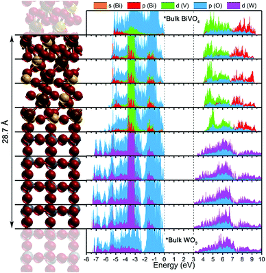
A layer projected density of states (LPDOS) was calculated for the WO3/BiVO4 heterojunction from the centre of one of the WO3 section to the centre of the BiVO4 section (Fig. 4). This highlighted the changes in the PDOS, layer-by-layer, on moving from the bulk-like section of each material to the interface. For comparison, the 2D PDOS of the central portion of isolated BiVO4 and WO3 slabs are included at the top and bottom respectively. The band gap energy in the WO3 layer is comparable to the experimental value, while the BiVO4 layer band gap is overestimated, as can expected by adopting 20% HF mixing in the B3LYP functional. To validate our band alignment results, the PDOS of the relaxed structure was calculated using PBE and HSE06 functionals (Fig. S15 & S16†). No substantial differences in band alignment were observed.
The LPDOS depicts an interfacial band alignment that somewhat differs from previous experimental reports (in which the band alignment was determined using electrochemical methods).22,27,50 On the atomic scales modelled herein, the conduction band shows a similar trend to those determined experimentally, i.e. a staggering in which the conduction band minimum of BiVO4 lies at a higher binding energy (more negative potential vs. NHE) with respect to the conduction band minimum of WO3; both at the interface and bulk-like regions. Contrary to experimental reports, the PDOS herein shows an alignment of the valence band maxima; again, both at the interface and bulk-like regions. Before continuing, we should first highlight the differences in the experimental determination of the band alignment and the computational study undertaken herein. By experiment, the energy of the valence band maximum is determined using indirect methods, where one takes the energy difference between the conduction band minimum (determined using electrochemical methods) and the optical band gap (determined using spectroscopic methods). Moreover, this is determined from the individual materials i.e. pure BiVO4 and WO3; not a WO3/BiVO4 heterojunction, where it is assumed that their coupling and formation of a junction does not alter interfacial band energies. Our calculations show that this is likely an oversimplification.
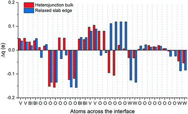
The valence band alignment observed in our LPDOS appears to be caused by strong cation hybridization of the d(W), d(V) and p(Bi) orbitals across the heterojunction as shown by alignment of the peaks at −3.5 eV (Fig. 4). The d(W) and d(V) peaks at −3.5 eV show a significant increase in intensity relative to the bulk-like material, whereas the p(Bi) peak forms a new ‘interface state’ within the heterojunction. Similarly, new d(W), d(V) and p(Bi) interfacial states arise at −1.5 eV and appear to be strongly hybridized. These new interfacial states may be a result of the Bi–O–W and V–O–W bonds that connect the two materials. Higher energy states have recently been observed in BiVO4 when V5+ was reduced to V4+,51 thus it is highly likely that this new higher energy hybridized state may be the result of increased electron density localized on V (or Bi) sites at the heterojunction interface. This was evidenced from our charge density difference calculations (Fig. 5). When the heterojunction is formed, cations at the interface in the BiVO4 layer possess higher electron density (Δq ∼ 0.05–0.1) and are thereby partly reduced relative to the bulk. However, cations at the interface in the WO3 layer possess lower electron density (−Δq ∼ 0.05–0.15) and are thereby partly oxidized relative to the bulk. This redistribution of charge will favour the transfer of photogenerated electrons, formed in the partly reduced BiVO4 region, into the partly oxidized WO3 region, as the conduction band minima are primarily formed from cationic orbitals.
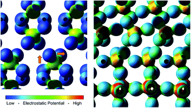
On moving several nanometers from the interface, hybridization d(W), d(V) and p(Bi) orbitals is maintained, which is attributed to the ordered growth of the BiVO4 layer on the WO3 (001) surface. Coincidently, it is observed that upon relaxation of the heterojunction, the VO43− tetrahedra reorient (Fig. 6), resulting in long-range orbital order that extrudes from the WO6 octahedra at the interface. It is likely that this chain of strong hybridization causes the valence band energies to pin, resulting in a non-staggered valence band. Evidence of hybridization and long-range order is also observed in the 3d electron charge density map (Fig. 6); the size and electrostatic potential of the oxygen orbitals does not change substantially throughout the heterojunction, suggesting that the nature of the common oxygen anion doesn't change significantly across the junction, and thus facilitates cation hybridization.
It is worth bearing in mind that when BiVO4 grows on top of WO3, the BiVO4 lattice will distort to match the WO3 lattice. Our models predict a 0.4% and 3.1% increase in the a and b lattice planes respectively. By comparing isolated slabs at bulk and heterojunction geometry (Fig. S17†), we find that this contributes to a widening of the BiVO4 band gap by ∼0.16 eV at the interface. This distortion likely contributes to the higher binding energy of the conduction band in BiVO4 at the heterojunction interface (more negative conduction band minimum vs. NHE), but it is not enough to entirely account for the offset which is in the range of 0.5–1 eV through the layers. This band gap widening effect will likely fade once the BiVO4 lattice reorients at further distances from the interface (i.e. several nanometers).
The band alignment determined from our LPDOS (Fig. 4) suggest a different model of the interfacial electronic structure from that determined using classical methods with experimental values (Fig. 3). Although the staggering of the conduction band energies is similar, our LPDOS shows that in both materials the valence band maximum lays at similar energy at the interface due to strong orbital hybridization (that will not favour hole separation across the interface), whereas a substantial difference in energy (∼0.7 eV) is present in the classical model (that will favour hole transfer from WO3 to BiVO4). As such, we believe our LPDOS model is more consistent with our experimental observations of photocatalytic performance. When the WO3/BiVO4 heterojunction is illuminated from the back, a greater portion of charges are formed in the WO3 layer (Fig. 2b). Holes formed in the WO3 layer need to cross the junction to reach the BiVO4/electrolyte interface and react; however, contrary to the classical model, our LPDOS shows that there is no thermodynamic energy gain to drive this process, nor is there a barrier to prevent holes from crossing back and recombining with concomitant electrons in the WO3 layer. This is consistent with our experimental measure of photocatalytic activity, where under back illumination our WO3/BiVO4 heterojunction showed substantially lower activity except for wavelengths that are primarily absorbed by the BiVO4 layer (Fig. 1b). Upon front illumination, both models can be used to rationalize the enhancement in photocatalytic performance found in the junction. The staggering of the conduction bands found in our LPDOS model are analogous to the classical model, and favours the transfer of photogenerated electrons, formed in the BiVO4 layer, to move into the WO3 layer, and inhibits their return and recombination with concomitant holes (Ea barrier ∼ 1 eV in our PDOS calculation; Ea barrier ∼ 0.4 eV in our classical model). When the WO3/BiVO4 junction is illuminated from the front, most of the charges are formed in the BiVO4 layer (Fig. 2a) and electrons are more efficiently extracted due to the favourable staggering of the conduction bands (Fig. 1a).
Conclusion
Recent studies have shown that the most effective strategy for enhancing the activity of water splitting devices (and other photocatalytic processes) is to form heterojunction systems. The key to this enhancement lies at the heterojunction interface, where charge separation occurs. To obtain insights into the interface that will enable the design of better performing water splitting devices, we develop a novel theoretical–experimental approach for the study of photocatalytic heterojunctions using the model system – WO3/BiVO4.Flat, dense WO3/BiVO4 heterojunction photoanodes were thus fabricated, and their photoelectrochemical performance towards water oxidation was measured. Under front illumination, the WO3/BiVO4 junction showed synergistically enhanced light-to-current conversion efficiencies (IPCE ∼ 25% at 400 nm for WO3/BiVO4vs. IPCE ∼ 10% at 400 nm for BiVO4). However, under back illumination, the WO3/BiVO4 junction showed overall lower light-to-current conversion efficiencies than BiVO4 alone (IPCE ∼ 10% at 400 nm for WO3/BiVO4vs. IPCE ∼ 12% at 400 nm for BiVO4), which appears to be related to energetic barriers for holes to cross the junction from WO3 into BiVO4.
To better understand the observed photoelectrochemical performance, the WO3/BiVO4 junction was modelled using two approaches: (i) a classical band bending model and (ii) a novel layer projected density of states (LPDOS) model calculated using Density Functional Theory (DFT). The band bending model showed that, in the absence of an applied potential, significant barriers exist for interfacial charge-carrier separation to occur, which may be overcome by tuning the donor densities of each layer. The LPDOS model, which is calculated from the atomic structure of the most likely heterojunction interface between the two materials; WO3 (001)/BiVO4 (001), revealed a non-staggered valence band maximum due to the hybridization of interfacial states. The formation of these new states across multiple atomic layers is attributed to the presence of oxygen anions in both materials, along with the strong tendency for the WO3 underlayer to direct the growth of the BiVO4 layer.
The presence of a non-staggered valence band indicates that the movement of photogenerated holes across the heterojunction interface is not favoured. The LPDOS model thus explains the experimentally observed photoelectrochemical performance under both front illumination (when electron transfer dictates/limits performance) and back illumination (when hole transfer dictates performance), whereas our classical model can only accurately describe the experimentally observed performance under front illumination.
These findings highlight the role that interfacial effects can play in defining the activity of heterojunction photocatalyst systems. We believe that the novel methodology developed herein for the study of such effects can serve as a template for future in-depth studies of efficient heterojunction systems. Our combined approach, using both experiment and theory, provides unique insight into the phenomena that arise at the interface when two semiconductor materials are brought together, such as the formation of interfacial states and band alignment, going far beyond traditional band bending models.
Conflicts of interest
There are no conflicts to declare.Acknowledgements
A. K. thanks Imperial College London for a Junior Research Fellowship and the Royal Society for a Research Grant (RSG\R1\180434). The authors thank Prof. James Durrant for useful discussions and access to photoelectrochemical equipment. J. R. D. thanks the ERC for financial support (project Intersolar 291482). Via our membership of the UK's HEC Materials Chemistry Consortium, which is funded by EPSRC (EP/L000202), this work used the ARCHER UK National Supercomputing Service (http://www.archer.ac.uk).Notes and references
- A. Fujishima and K. Honda, Nature, 1972, 238, 37–38 CrossRef CAS PubMed.
- A. J. Cowan and J. R. Durrant, Chem. Soc. Rev., 2013, 42, 2281–2293 RSC.
- S. Hejazi, N. T. Nguyen, A. Mazare and P. Schmuki, Catal. Today, 2017, 281, 189–197 CrossRef CAS.
- A. U. Pawar, C. W. Kim, M. J. Kang and Y. S. Kang, Nano Energy, 2016, 20, 156–167 CrossRef CAS.
- A. Kafizas, L. Francàs, C. Sotelo-Vazquez, M. Ling, Y. Li, E. Glover, L. McCafferty, C. Blackman, J. Darr and I. Parkin, J. Phys. Chem. C, 2017, 121, 5983–5993 CrossRef CAS.
- S. Wang, P. Chen, J.-H. Yun, Y. Hu and L. Wang, Angew. Chem., 2017, 129, 8620–8624 CrossRef.
- A. Paracchino, V. Laporte, K. Sivula, M. Grätzel and E. Thimsen, Nat. Mater., 2011, 10, 456–461 CrossRef CAS PubMed.
- P. Dias, A. Vilanova, T. Lopes, L. Andrade and A. Mendes, Nano Energy, 2016, 23, 70–79 CrossRef CAS.
- J. Luo, L. Steier, M.-K. Son, M. Schreier, M. T. Mayer and M. Grätzel, Nano Lett., 2016, 16, 1848–1857 CrossRef CAS PubMed.
- J. Su, L. Guo, N. Bao and C. A. Grimes, Nano Lett., 2011, 11, 1928–1933 CrossRef CAS PubMed.
- M. Liu, N. de Leon Snapp and H. Park, Chem. Sci., 2011, 2, 80–87 RSC.
- J. R. Bolton, S. J. Strickler and J. S. Connolly, Nature, 1985, 316, 495–500 CrossRef CAS.
- C. Sotelo-Vazquez, R. Quesada-Cabrera, M. Ling, D. O. Scanlon, A. Kafizas, P. K. Thakur, T.-L. Lee, A. Taylor, G. W. Watson, R. G. Palgrave, J. R. Durrant, C. S. Blackman and I. P. Parkin, Adv. Funct. Mater., 2017, 27, 1605413 CrossRef.
- W. Feng, L. Lin, H. Li, B. Chi, J. Pu and J. Li, Int. J. Hydrogen Energy, 2017, 42, 3938–3946 CrossRef CAS.
- Y. Li, J. Feng, H. Li, X. Wei, R. Wang and A. Zhou, Int. J. Hydrogen Energy, 2016, 41, 4096–4105 CrossRef CAS.
- C. G. Morales-Guio, L. Liardet, M. T. Mayer, S. D. Tilley, M. Grätzel and X. Hu, Angew. Chem., Int. Ed., 2015, 54, 664–667 CAS.
- Q. Wang, T. Hisatomi, Q. Jia, H. Tokudome, M. Zhong, C. Wang, Z. Pan, T. Takata, M. Nakabayashi, N. Shibata, Y. Li, I. D. Sharp, A. Kudo, T. Yamada and K. Domen, Nat. Mater., 2016, 15, 611–615 CrossRef CAS PubMed.
- X. Liu, F. Wang and Q. Wang, Phys. Chem. Chem. Phys., 2012, 14, 7894 RSC.
- Y. Pihosh, I. Turkevych, K. Mawatari, J. Uemura, Y. Kazoe, S. Kosar, K. Makita, T. Sugaya, T. Matsui, D. Fujita, M. Tosa, M. Kondo and T. Kitamori, Sci. Rep., 2015, 5, 11141 CrossRef PubMed.
- C. Fàbrega, S. Murcia-López, D. Monllor-Satoca, J. D. Prades, M. D. Hernández-Alonso, G. Penelas, J. R. Morante and T. Andreu, Appl. Catal., B, 2016, 189, 133–140 CrossRef.
- T. W. Kim and K.-S. Choi, Sci. 80, 2014, 343, 990–994 CrossRef CAS PubMed.
- Y. Pihosh, I. Turkevych, K. Mawatari, T. Asai, T. Hisatomi, J. Uemura, M. Tosa, K. Shimamura, J. Kubota, K. Domen and T. Kitamori, Small, 2014, 10, 1–8 CrossRef PubMed.
- X. Shi, I. Herraiz-Cardona, L. Bertoluzzi, P. Lopez-Varo, J. Bisquert, J. H. Park and S. Gimenez, Phys. Chem. Chem. Phys., 2016, 18, 9255–9261 RSC.
- M. G. Mali, H. Yoon, M. Kim, M. T. Swihart, S. S. Al-Deyab and S. S. Yoon, Appl. Phys. Lett., 2015, 106, 151603 CrossRef.
- I. Grigioni, K. G. Stamplecoskie, E. Selli and P. V. Kamat, J. Phys. Chem. C, 2015, 119, 20792–20800 CrossRef CAS.
- S. S. Kalanur, I.-H. Yoo, J. Park and H. Seo, J. Mater. Chem. A, 2017, 5, 1455–1461 RSC.
- S. J. Hong, S. Lee, J. S. Jang and J. S. Lee, Energy Environ. Sci., 2011, 4, 1781 RSC.
- T. Bredow, K. Jug and R. A. Evarestov, Phys. Status Solidi, 2006, 243, R10–R12 CrossRef CAS.
- F. Wang, C. Di Valentin and G. Pacchioni, J. Phys. Chem. C, 2011, 115, 8345–8353 CrossRef CAS.
- R. Weihrich and I. Anusca, Z. Anorg. Allg. Chem., 2006, 632, 335–342 CrossRef CAS.
- M. F. Peintinger, D. V. Oliveira and T. Bredow, J. Comput. Chem., 2013, 34, 451–459 CrossRef CAS PubMed.
- C. L. Bailey, L. Liborio, G. Mallia, S. Tomić and N. M. Harrison, Phys. Rev. B: Condens. Matter Mater. Phys., 2010, 81, 205214 CrossRef.
- G. C. De Fusco, L. Pisani, B. Montanari and N. M. Harrison, Phys. Rev. B: Condens. Matter Mater. Phys., 2009, 79, 085201 CrossRef.
- J. Muscat, A. Wander and N. M. Harrison, Chem. Phys. Lett., 2001, 342, 397–401 CrossRef CAS.
- G. Mallia and N. M. Harrison, Phys. Rev. B: Condens. Matter Mater. Phys., 2007, 75, 165201 CrossRef.
- E. A. Ahmad, L. Liborio, D. Kramer, A. R. Kucernak, G. Mallia and N. M. Harrison, Phys. Rev. B: Condens. Matter Mater. Phys., 2011, 84, 085137 CrossRef.
- Y. Ma, S. R. Pendlebury, A. Reynal, F. le Formal and J. R. Durrant, Chem. Sci., 2014, 5, 2964 RSC.
- K. Sayama, A. Nomura, T. Arai, T. Sugita, R. Abe, T. Oi, Y. Iwasaki, Y. Abe and H. Sugihara, J. Phys. Chem. B, 2006, 110, 11352–11360 CrossRef CAS PubMed.
- I. A. Castro, G. Byzynski, M. Dawson and C. Ribeiro, J. Photochem. Photobiol., A, 2017, 339, 95–102 CrossRef CAS.
- K. Zhang, X.-J. Shi, J. K. Kim and J. H. Park, Phys. Chem. Chem. Phys., 2012, 14, 11119 RSC.
- K. P. S. Parmar, H. J. Kang, A. Bist, P. Dua, J. S. Jang and J. S. Lee, ChemSusChem, 2012, 5, 1926–1934 CrossRef CAS PubMed.
- L. Han, F. F. Abdi, R. van de Krol, R. Liu, Z. Huang, H.-J. Lewerenz, B. Dam, M. Zeman and A. H. M. Smets, ChemSusChem, 2014, 7, 2832–2838 CrossRef CAS PubMed.
- F. F. Abdi, L. Han, A. H. M. Smets, M. Zeman, B. Dam and R. Van De Krol, Nat. Commun., 2013, 4, 2195 CrossRef PubMed.
- J. Wiktor, I. Reshetnyak, F. Ambrosio and A. Pasquarello, Phys. Rev. Mater., 2017, 1, 022401 CrossRef.
- I. N. Yakovkin and M. Gutowski, Surf. Sci., 2007, 601, 1481–1488 CrossRef CAS.
- F. Wang, C. Di Valentin and G. Pacchioni, J. Phys. Chem. C, 2012, 116, 10672–10679 CrossRef CAS.
- G. Xi and J. Ye, Chem. Commun., 2010, 46, 1893 RSC.
- H. Ullah, A. A. Tahir and T. K. Mallick, Appl. Catal., B, 2018, 224, 895–903 CrossRef CAS.
- S. N. F. M. Nasir, H. Ullah, M. Ebadi, A. A. Tahir, J. S. Sagu and M. A. Mat Teridi, J. Phys. Chem. C, 2017, 121, 6218–6228 CrossRef CAS.
- S. Y. Chae, C. S. Lee, H. Jung, O.-S. Joo, B. K. Min, J. H. Kim and Y. J. Hwang, ACS Appl. Mater. Interfaces, 2017, 9, 19780–19790 CrossRef CAS PubMed.
- T. Liu, X. Zhou, M. Dupuis and C. Li, Phys. Chem. Chem. Phys., 2015, 17, 23503–23510 RSC.
Footnote |
| † Electronic supplementary information (ESI) available. See DOI: 10.1039/c8se00420j |
| This journal is © The Royal Society of Chemistry 2019 |

