
Giant magneto-optical response in H+ irradiated Zn1−xCoxO thin films
G.
Varvaro
 a,
A.
Di Trolio
*a,
A.
Polimeni
b,
A.
Gabbani
c,
F.
Pineider
cd,
C.
de Julián Fernández
e,
G.
Barucca
f,
P.
Mengucci
f,
A.
Amore Bonapasta
a and
A. M.
Testa
a
a,
A.
Di Trolio
*a,
A.
Polimeni
b,
A.
Gabbani
c,
F.
Pineider
cd,
C.
de Julián Fernández
e,
G.
Barucca
f,
P.
Mengucci
f,
A.
Amore Bonapasta
a and
A. M.
Testa
a
aCNR-Istituto di Struttura della Materia, Via Salaria Km, 29,300 00015 Monterotondo St., Roma, Italy. E-mail: antonio.ditrolio@cnr.it
bDipartimento di Fisica, Universita’ di Roma “La Sapienza”, P.le A. Moro 2, 00185 Roma, Italy
cDipartimento di Chimica e Chimica Industriale, Università di Pisa, Via Moruzzi 13, 56124 Pisa, Italy
dDipartimento di Chimica “Ugo Schiff”, Università degli Studi di Firenze, Via della Lastruccia 3, 50019 Sesto Fiorentino, FI, Italy
eCNR, IMEM, Parma, Italy
fDipartimento di Scienze e Ingegneria della Materia, dell'Ambiente ed Urbanistica – SIMAU, Università Politecnica delle Marche, Via Brecce Bianche 12, 60131 Ancona, Italy
First published on 21st November 2018
Abstract
Remarkable improvements in the magneto-optical properties of Zn1−xCoxO thin films were achieved by post-growth hydrogen irradiation at temperatures of 400 °C. Hydrogen incorporation increases the magnetic circular dichroism signal resulting in large values of ellipticity and Faraday rotation at room temperature. The hysteretic behavior of the magneto-optical field dependent loops at different sub-bandgap wavelengths indicates an intrinsic ferromagnetic regime. A giant Faraday rotation of 3000 deg cm−1 was observed at 400 nm. Optical, structural and microstructural characterizations pointed out the Zn substitution by Co, ruling out the presence of noticeable Co-related secondary phases down to the nanoscale. The increased values of saturation magnetization, ellipticity and Faraday rotation have been explained based on an impurity band close to the conduction band minimum, which is induced by Co–VO (O vacancies) complexes. A phenomenological model founded on such an impurity band and electronic states induced by other Co-defect complexes in the ZnO energy gap allows a thoroughly novel, fine interpretation of the ellipticity spectra.
1. Introduction
Future nonreciprocal photonic components, exploiting the difference between the original input and the final output of light in a bidirectional transmission path (optical nonreciprocity), are indispensable components in optical communications systems.1 The breaking of such bidirectional transmission reciprocity of light is achieved by using materials exhibiting a magneto-optical (MO) effect, which is able to rotate the polarization plane of the transmitted (reflected) light by the Faraday (Kerr) effect in spectral regions where the optical absorption is negligible.From the materials point of view, exploring improved MO thin film materials with a high figure of merit (i.e. high ratio of Faraday rotation (FR) per unit length to the optical loss per unit length) can pave the way for development of new integrated on-chip nonreciprocal photonic devices, such as optical circulators, isolators and directional amplifiers which are based on the Faraday effect.1–3 Garnets are the current material solution for such MO devices due to their low optical absorption and extremely high FR ranging from 3–5 × 10³ deg cm−1 (yttrium iron garnet, YIG) to 8 × 10⁴ deg cm−1 (bismuth iron garnet), at 633 nm.3–5 However, the integration of garnets in optical semiconductor circuits is a challenge due to the incompatibility between the film deposition and device fabrication processes. First of all, garnets have a complex unit cell structure and a much larger lattice parameter compared with semiconductors (YIG: 12.376 Å, Si: 5.43 Å, GaAs: 5.65 Å), which excludes the possibility of hetero-epitaxial growth of garnet films on a conventional semiconductor substrate. Secondly, the thermal expansion coefficient of YIG (10.4 × 10⁻⁶ °C−1) is much larger than that of Si (2.3 × 10⁻⁶ °C−1), GaAs (5.7 × 10⁻⁶ °C−1), InP (4.7 × 10⁻⁶ °C−1), and ZnO (5.0 × 10⁻⁶ °C−1): cracks can easily generate in the crystallized YIG films on silicon when the thickness exceeds the critical value of about 100 nm.6 Thirdly, crystallization of the garnet phase usually requires an annealing treatment at high temperature (700–800 °C): impurity phases such as YFeO3, Fe2O3 and Bi2O3 can precipitate out during the crystallization process, which may cause optical scattering loss in integrated photonic devices. Hence, such factors make the fabrication of high optical quality magnetic garnet films and also optical isolators on semiconductor substrates very difficult.7
A promising alternative to garnet films is represented by diluted magnetic semiconductors (DMS) which are a platform for device integration. In such context, wide gap ZnO-based DMS obtained by incorporating transition metal elements (e.g. Fe, Co) are suitable for the purpose. In particular, for Co-doped ZnO (Zn1−xCoxO) thin films it has been shown that a large enhancement in the ferromagnetic behavior can be induced by suitable atomic hydrogen treatment, without the formation of metal Co nanophases.8–11
In the context of DMS, the MO effect is useful to investigate the strength and the nature of ferromagnetism as arising from spin polarized carriers magnetically coupled to magnetic ions. However, due to the presence of a finite optical absorption, the polarization of the transmitted light rotates and turns from linear (i.e. superposition of left (LCP) and right circularly polarized components (RCP)) to elliptical. Hence, in general terms the MO effect can be described by a complex rotation whose real and imaginary parts are represented by FR (rotation) and ellipticity (absorption), respectively.
Such quantities provide information about the allowed optical transitions among the electronic states at energy E split by the magnetic field, according to the Zeeman effect. The MO effect was previously observed in Zn1−xCoxO films mainly at low temperatures.11–13 There are also reports of MCD at room temperature with hysteretic behavior at the band edge14 and measurements of MCD after the exposure to Zn metal vapor in a wide sub-bandgap range.15 To our knowledge the Faraday effect was not observed in Zn1−xCoxO yet, although literature results exist in the case of Ti-doped ZnO for photon energies larger than 3 eV.14
In this work, the role of hydrogen in the optical and magneto-optical properties of ferromagnetic Zn1−xCoxO films has been addressed by measuring the MCD spectra of the films irradiated by hydrogen ions. The ferromagnetic nature of the magnetic interaction has been investigated by obtaining room temperature hysteresis loops exploiting the field dependence of the MO effect at different wavelengths in the sub-bandgap region. For the samples irradiated with a high H-dose we also measured the FR, which is fundamental for MO device applications, at room temperature and visible-NIR range. Increased values of saturation magnetization, ellipticity and Faraday rotation are observed, which can be explained by the existence of an impurity band close to the conduction band minimum, induced by Co–VO (O vacancies) complexes, combined with an increase of negative carriers induced by shallow donors,8 that are, in the present case, H-related defects. A phenomenological model founded on such an impurity band and electronic states induced by other Co-defect complexes in the ZnO energy gap allows a thoroughly novel, fine interpretation of the ellipticity spectra.
2. Experimental
Thin Zn1−xCoxO films, hereafter referred to as D0, LD1, LD2, HD1, and HD2 were deposited by pulsed laser deposition using a Nd:YAG laser, operating at λ = 355 nm, fluence ∼2 J cm−2 and 10 Hz repetition rate, starting from Zn1−xCoxO pellets with a nominal Co content, x = 0.05. These films were grown on optically transparent Al2O3(001) single crystal substrates placed at a distance of 5 cm from the target, at 500 °C and 2 × 10⁻⁵ mbar O2 pressure with a growth rate of ca. 4 Å s−1. The averaged thickness values of D0, HD1, HD2, LD1, and LD2 determined by SEM and TEM measurements, are 420, 400, 430, 330, and 330 nm, respectively. The thickness uncertainties, mainly due to the film roughness, are within 10%. Subsequently, films HD1, HD2, LD1, and LD2 were irradiated with a beam of hydrogen ions produced by a Kaufman source. Hydrogen diffusion in the sample depth was promoted by maintaining the samples at 400 °C during the hydrogenation process with H-beam exposure ranging from 2 to 5 h. The energy of the H-ions was equal to 100 eV with current densities in the order of tens of μA cm−2. The HD1 and HD2 films were irradiated with a H+ dose of 4.5 × 10¹⁸ ions per cm2 (HD), LD1 and LD2 with 1.5 × 10¹⁸ ions per cm2 (LD), whereas D0 is the unirradiated film. We considered a couple of samples for both the H-doses to better highlight the effect of the H irradiation on the MO properties of the Zn1−xCoxO films. The fabrication parameters, thickness and H-dose of all the samples are reported in Table 1.| D0 | LD1 | LD2 | HD1 | HD2 | |
|---|---|---|---|---|---|
| deposition T (°C) | 500 | 500 | 500 | 500 | 500 |
| O2 pressure (mbar) | 2 × 10⁻⁵ | 2 × 10⁻⁵ | 2 × 10⁻⁵ | 2 × 10⁻⁵ | 2 × 10⁻⁵ |
| Thickness (nm) | 420 | 330 | 330 | 400 | 430 |
| H-dose (ions per cm2) | 0 | 1.5 × 10¹⁸ | 1.5 × 10¹⁸ | 4.5 × 10¹⁸ | 4.5 × 10¹⁸ |
XRD measurements were performed on a Bruker D8 Advance diffractometer in Bragg–Brentano geometry using the Cu-Kα radiation (λ = 1.5406 Å), with diffracted intensities collected in a θ–2θ scan. Scanning electron microscopy (SEM) analysis measurements were performed using a Zeiss SUPRA40 scanning electron microscope equipped with a field emission gun. Samples were observed without any preparation. The thickness of the Zn1−xCoxO films was measured by vertically mounting the samples on a home-made SEM holder. Transmission electron microscopy (TEM) observations were carried out using a Philips CM200 electron microscope equipped with a LaB6 filament and operating at 200 kV. For TEM cross-sectional observations, samples were prepared by the conventional thinning procedure consisting of mechanical polishing using grinding paper, diamond paste, and a dimple grinder. Final thinning was carried out using an ion beam system (Gatan PIPS) using Ar ions at 5 kV. Field-dependent magnetization measurements were performed at 300 K using a Micro Sense Model-10 VSM magnetometer with a max field of 20 kOe. Room temperature optical transmittance spectra were acquired using a Jasco V670 spectrophotometer. The MO properties were investigated by using a home-built apparatus capable of performing measurements in the wavelength range of 350–850 nm in magnetic circular dichroism configuration and 350–850 nm in the Faraday rotation configuration, under magnetic fields up to 1.3 T.16
3. Results and discussion
3.1 Structural, microstructural and magnetic properties
XRD patterns of the blank substrate as well as patterns of the D0, HD1 and LD1 films, respectively treated with zero (untreated), high and low H-dose, are shown in Fig. 1. No major structural change occurs, according to our previous results.8 The substrate is Al2O3(001) single crystal, while all films are hexagonal ZnO (zincite). No other phases (metallic Co, Co oxides) were detected. The films show a (001) preferential orientation, with the c-axis of the hexagonal lattice perpendicular to the Al2O3 substrate. The presence of a single ZnO peak in the XRD pattern suggests a columnar growth of the ZnO grains through the entire film thickness. Peak shape analysis of the XRD patterns allowed obtaining the exact angular position of the ZnO(002) peak, which provides the value of the c lattice parameter of ZnO. The results show that the c lattice parameters of the films are about 0.2–0.4% higher than the nominal value of the ZnO compound reported in the ICDD file (no. 36-1451). Furthermore, the full width at half maximum (FWHM) of the ZnO(002) peak can be used in the Scherrer formula to estimate the average grain size of the films. In this case, due to the columnar growth, the Scherrer formula allowed estimating the average lateral size of the columnar grains forming the entire film. For the Zn1−xCoxO films investigated, the average lateral size of the columnar grains ranges between 40 and 100 nm.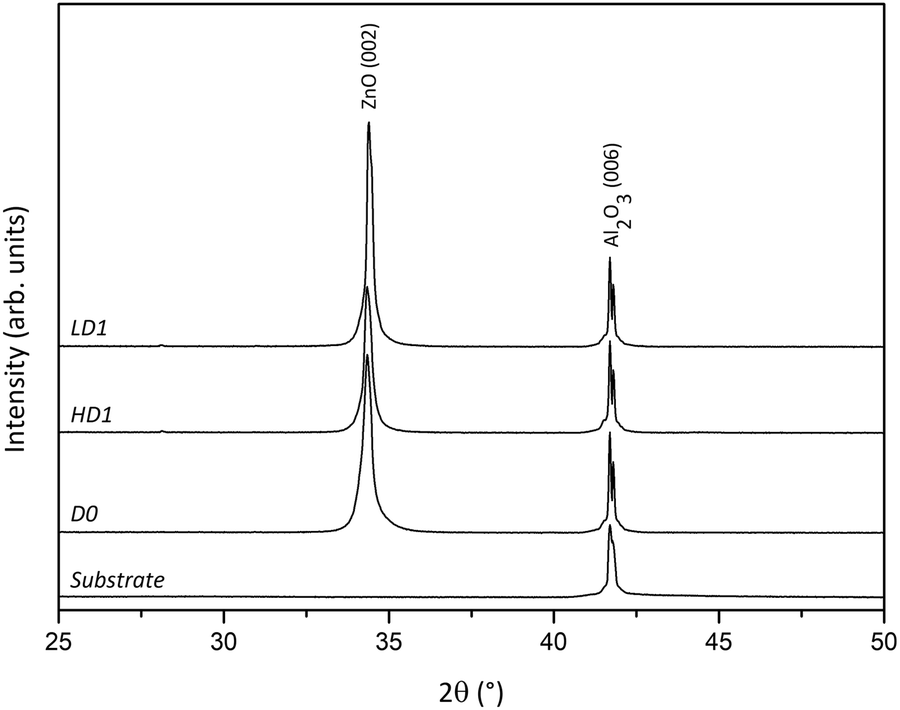 | ||
| Fig. 1 XRD patterns of D0, HD1 and LD1 films, treated with zero, high and low H-dose, respectively. Pattern of the blank substrate is also shown. Patterns are vertically shifted for clarity. | ||
Films thickness, morphology, and microstructure were investigated by SEM and TEM analyses. Fig. 2a and c show typical TEM bright field images of the HD2 and LD2 samples respectively. Both films consist of columnar grains having lateral size ranging from 30 to 80 nm. Selected area electron diffraction (SAED) measurements revealed an oriented growth of the Zn1−xCoxO films on the alumina substrate with the following orientation relationships: [010]ZnO//[−110]Al2O3 and (001)ZnO//(001)Al2O3, for the HD2 sample, Fig. 2b, and [−110]ZnO//[−110]Al2O3 and (001)ZnO//(001)Al2O3 for LD2, Fig. 2d. The two samples have the c axis perpendicular to the substrate in perfect agreement with the diffraction peaks in XRD spectra.
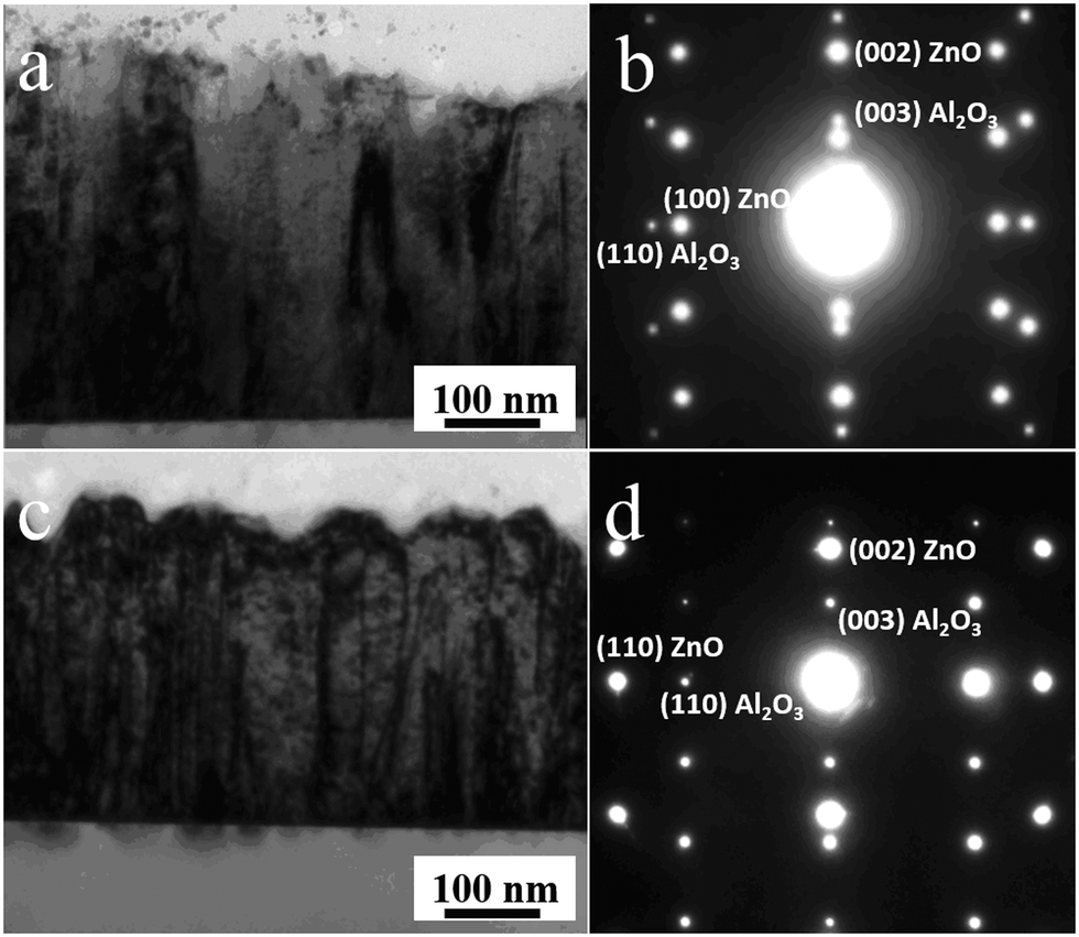 | ||
| Fig. 2 Bright field TEM images and corresponding SAED patterns taken in the [−110] Al2O3 zone axis of: HD2 (a and b) and LD2 (c and d) samples. | ||
High resolution TEM observations, performed in different areas of the samples, did not reveal the presence of second phase precipitates confirming the XRD analysis, albeit crystal defects present. In particular, Fig. 3 shows the typical atomic structure of the [010] ZnO film in the HD2 sample. The atomic order is retained moving from one grain to another and the Fourier analysis of the images (FFT) has never revealed the presence of other phases. The inset of Fig. 3 was obtained by removing the noise from the image by using the Gatan Microscopy Suite GMS3 software [http://www.gatan.com/products/tem-analysis/gatan-microscopy-suite-software]. The typical approach consists of the FFT of the image, the application of a mask to remove the noise and an inverse FFT to reobtain the image. The atomic periodicity in the alumina substrate and the film is clearly evidenced in this way, and it is possible to observe the nature of the interface. In detail, the right side of the inset shows that there are zones in which a good match of the lattice cells is present at the interface, but due to the lattice parameters differences, the ZnO cell tends to expand in other zones during the film growth, with the formation of a disordered interface, left side of the inset. The large variation in the image contrast can be attributed to the presence of point defects connected to the Co introduction in the lattice.17,18
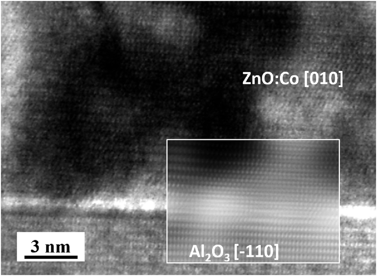 | ||
| Fig. 3 High resolution TEM image of the HD2 sample taken in the [010]ZnO zone axis. The inset was obtained removing the image noise to evidence the sample interface. | ||
Fig. 4 shows the field-dependent magnetization loops at T = 300 K of the samples irradiated with the low and high H-doses. According to our previous results a high H dose can induce large values of the saturation magnetization.8 Indeed, starting from saturation magnetization (Ms) values lower than 1 emu cm−3 for the non-irradiated sample D0, Ms reaches values of 2–4 emu cm−3 for LD1 and LD2, and 10–12 emu cm−3 for HD1 and HD2. This large enhancement of Ms supports the results of a previous study8 where the ferromagnetic behavior of Zn1−xCoxO was attributed to the formation of Co–VO (oxygen vacancy) complexes and to an increase of the negative carriers induced by shallow donors represented here by H-related defects, like H at the VO site (HO) and H interstitials (HI).
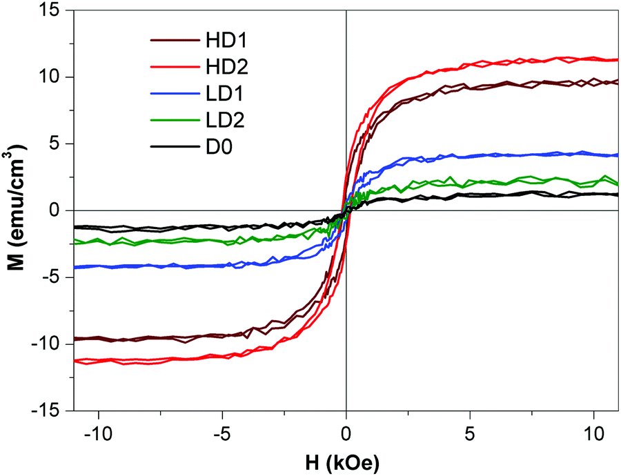 | ||
| Fig. 4 Room temperature hysteresis curves of zero, low and high H-dose irradiated films. | ||
3.2 Optical and magneto-optical properties
Fig. 5 shows the transmittance curves (a) and the MCD spectra, calibrated in degrees (ellipticity) and normalized to the thickness (b), at room temperature and applied field of 1.3 T, of Zn1−xCoxO films after the correction of substrate contribution. MO measurements were focussed on the H-treated films. Both transmittance and ellipticity spectra exhibit a rapid increase near the band edge and a broad positive zone in the visible range of up to 850 nm in the NIR region, with some features near 600 nm. All transmission spectra show absorption dips at about 566, 613, and 660 nm, originating from the 4A2(F) → 2A1(G), 4A2(F) → 4T1(P), 4A2(F) → 2E(G) transitions of the tetrahedrally coordinated Co2+ ions, respectively.11,19,20 This clearly indicates that the added Co2+ ions have substituted Zn2+ cations without distorting the wurtzite structure in agreement with the results of the structural characterization.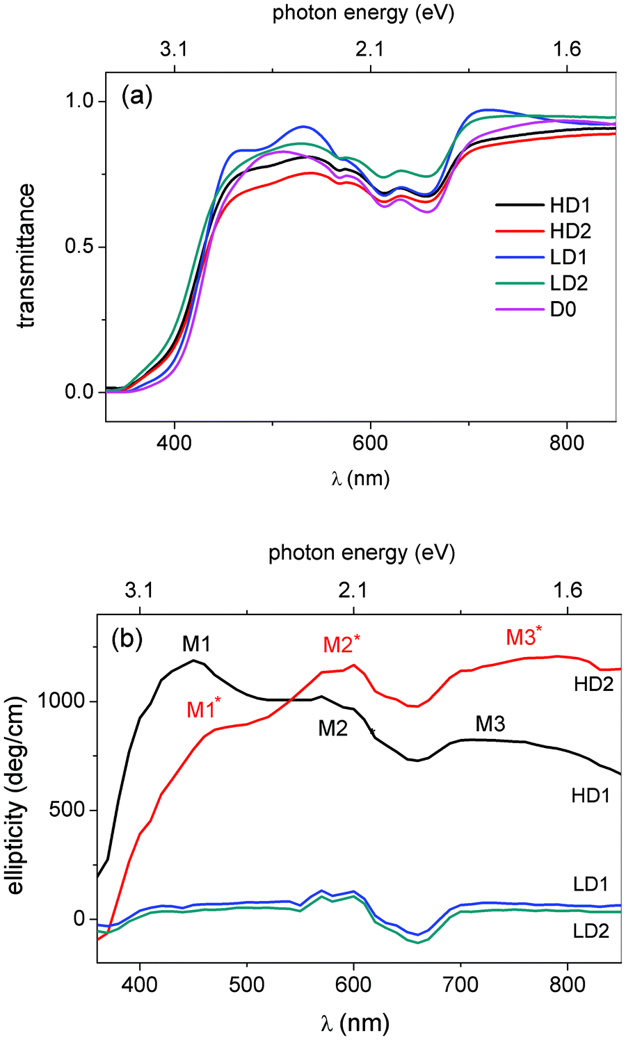 | ||
| Fig. 5 Transmittance ((a), upper panel) and ellipticity spectra ((b), lower panel) of the Zn1−xCoxO samples (see text). | ||
It is worth noting that, unlike the transmittance curves which are quite independent of the H doping, ellipticity sharply increases on increasing the hydrogen content, coherently with the magnetization measurements. In fact, starting from values of about 100 deg cm−1 for LD1 and LD2 samples, the ellipticity exceeds 1000 deg cm−1 for the HD1 and HD2 samples in the range of 400–600 nm. This large positive value directly indicates that the electronic states involved in the optical transitions are strongly influenced by the magnetic interaction leading to a large level splitting. Hence a large difference in the absorption of LCP and RCP light is expected.
In order to rule out any paramagnetic character of the ion–carrier interaction we measured the ellipticity as a function of magnetic field for the HD2 sample at different wavelengths, starting from the band edge up to 850 nm, in the near-IR region. As shown in Fig. 6 all the cycles show a clear ferromagnetic behavior. The curves are hysteretic with ellipticity values at saturation ranging from 200 to 1200 deg cm−1 and coercive fields of about 200 Oe, that well agree with the values of the magnetization measurements. In the sub-bandgap region (λ > 375 nm), the saturated ellipticity is observed to increase with λ up to 600 nm, where a value of 1200 deg cm−1 is found, keeping high values except for λ values corresponding to the optical absorption of Co2+ ions.
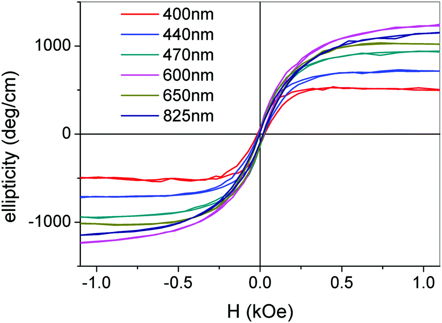 | ||
| Fig. 6 Magneto-optic hysteresis cycles of the HD2 films at room temperature, taken for different sub-bandgap wavelengths, starting from λ = 400 nm. | ||
The hysteretic character of the ellipticity curves confirms the intrinsic nature of the ferromagnetic coupling arising from a spin dependent band structure with the interaction between the carriers and localized spin of the magnetic ions. In the Zn1−xCoxO case the Co ions cannot sustain magnetic interactions beyond their first neighbours,21 whereas Co–VO complexes can promote long-range ferromagnetic order, if additional n-doping is present.21–23 Accordingly, the strength of the magnetic interaction increases by filling the half-empty donor-like band due to Co–VO complexes with carriers arising from donor defects.22,23 Hence the higher MCD values for the films treated with high H-doses well agrees with the proposed model as H-irradiation induces additional carriers and favors the formation of VO defects.8
By considering that the ellipticity rapidly increases near the band edge and keeps high values in the sub-bandgap region, we associate the ellipticity values to photoionization transitions involving electronic states induced by Co-defect complexes in the ZnO energy gap.15,24
The HD1 and HD2 ellipticity spectra of Fig. 5 (bottom panel) show different shapes characterized by different relative maxima located approximately at 430 nm (2.88 eV), 600 nm (2.10 eV), and in the range of 700–800 nm (1.77–1.55 eV). The fine structures of such spectra can be explained by a phenomenological model founded on previous theoretical studies25 and on a recent Kelvin Probe Force Microscopy (KPFM) investigation of Zn1−xCoxO samples26 giving indications about the levels induced by complexes formed by Co atoms and defects like VO's in the ZnO electronic structure. Such levels are schematically reported in Fig. 7. The d levels of a Co atom substituting the Zn atom (3d7) are split by the crystal fields induced by its four O neighbors in the filled e2g(↑)2 and t2g(↑)3 majority spin states located in the valence band, a filled e2g(↓)2 minority spin about 0.6 eV above the top of the valence band (TVB), and a t2g(↓) minority spin empty state at about 3 eV above the conduction band minimum (CBM), t2g(↓)-Co, not reported in Fig. 7. When a VO defect and a Co atom form a Co–VO complex, the t2g(↓)-Co state significantly lowers in energy, about 1.5 eV, since the crystal field is weakened by the removal of an O neighbor. Moreover, when populated by electrons provided by unintentional shallow donors (responsible of the n-type character of as grown ZnO), this t2g(↓) state further descents down to the CBM and partially mix with the CBM itself, t2g(↓)-VO in Fig. 7.23 Finally, a recent KPFM study showed a significant Fermi level lowering of about 0.4 eV in Zn1−xCoxO, indicating the presence of Co-induced deep levels in the ZnO energy gap. Such levels have been related to the formation of Co-defects (Co–D) complexes enhancing the Co under-coordination already realized in the Co–VO complex, thus inducing a further lowering of the t2g(↓) state, now indicated as the t2g(↓)-D state in Fig. 7.26 Then, by disregarding the t2g(↓)-Co state too high in energy, the Co–VO and Co–D complexes may induce two electronic states close to the CBM and in the energy gap, respectively, that, under illumination with light of suitable wavelength (approximately in the range of 3.0–1.5 eV), become empty or partially occupied and therefore available for internal d–d optical transitions starting from the e2g(↓) filled states common to Co and its complexes.
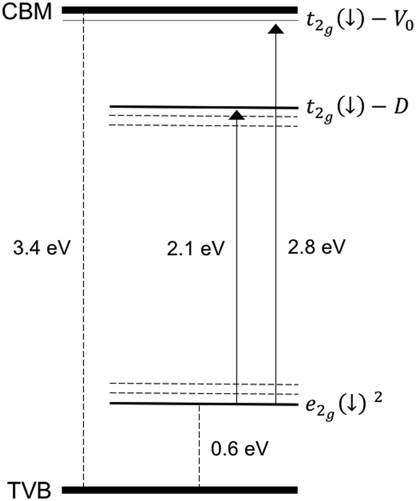 | ||
| Fig. 7 Schematic diagram showing electronic states induced by Co–VO and Co–D complexes (see the text) in the ZnO energy gap. TVB and CBM indicate the top of the valence band and the conduction band minimum, respectively. | ||
Let us note that the experimental and theoretical results23 locate the t2g(↓)-VO state very close to the CBM, whereas the mentioned KPFM results permit to locate the t2g(↓)-D states only quite below the Fermi energy. They are roughly located at 0.7 eV below the CBM in Fig. 7. Moreover, the Co–D complex represents a family of complexes where the Co atom undergoes different degrees of under-coordination. This implies a dispersion of these states, as well as of the corresponding e2g(↓) filled states, in a certain range of energy as schematized by the dashed lines in the same figure. Now, a phenomenological interpretation of the HD1 and HD2 ellipticity spectra can be attempted based on the electronic states sketched in Fig. 7 and assuming different relative concentrations of the Co–VO and Co-D complexes in the HD1 and HD2 samples. In detail, in the high energy side, the ellipticity signals of the HD1 sample reach a first maximum value M1 at about 430 nm, when the transmission of light becomes high (E < 3 eV) (the MCD measurement is performed in transmission) and the photon energy corresponds to the energy required to bring e2g(↓) electrons to the corresponding t2g(↓)-VO level, about 2.8 eV higher in energy (430 nm). As soon as the energy becomes small for such transitions the ellipticity signals of HD1 decrease and then reach a second, relative maximum (M2) at about 580 nm, 2.1 eV, that may correspond to the transitions e2g(↓) → t2g(↓)-D. Then, a further signal decrease is followed by reaching the third relative maximum (M3) corresponding to a sort of plateau in the range of 700–800 nm, that is, 0.4–0.6 eV below the M2 peak. This range may still correspond to e2g(↓) → t2g(↓)-D once the small dispersion in energy of the e2g(↓) and t2g(↓)-D states, shown in Fig. 7, is taken into account. The different amplitudes of the M1, M2, and M3 peaks can be accounted for by a predominant presence of the Co–VO complexes with respect to the Co-D ones in the HD1 sample. In the case of the HD2, the ellipticity signals show, basically at the same energies of the M1, M2, and M3 maxima, three corresponding, relative maxima M1*, M2*, and M3*. These peaks correspond therefore to the same transitions explaining the HD1 spectrum, while the different MX vs. MX* amplitudes may be accounted for by different relative concentrations of the Co–VO and Co-D complexes in the two samples, the latter complex being the predominant one in the HD2 sample.
In addition, the ellipticity also receives contributions from the differential absorption of RCP and LCP light at 566, 613, and 660 nm, related to the optical Zeeman-split d*–d transitions. We observe a broad positive signal ensuing ferromagnetic nature (as it can be observed from the hysteretic behaviour of the curves of Fig. 6) although the signal decrease around 600 nm indicates competing contributions to the ellipticity from d*–d. From the inspection of Fig. 5b it can be seen that the ellipticity of the LD1 and LD2 samples at around 600 nm takes negative values. This indicates that the main contribution to the ellipticity arises from the optical d*–d transitions as H-dose and hence the carrier density in LD1 and LD2 are consistently lowered with respect to HD1 and HD2, thus reducing the photoionization.
To fully investigate the MO response of the H-irradiated Zn1−xCoxO films we also measured the complex Faraday rotation spectra at saturation (1.3 T) for unirradiated D0, and low (high) H-dose treated sample LD1 (HD2). It turns out that the MO response of D0 is quite negligible, whereas LD1 and HD2 exhibit a sizeable effect, reaching a giant value for HD2. This is a further proof of the effectiveness of the H irradiation in modifying the electronic structure of the Zn1−xCoxO and hence its MO response. Focusing on the HD2 sample both rotation and ellipticity are reported as a function of λ in the inset of Fig. 8. The MO response consists of two main regions with different characteristics: a pure rotatory regime from the band edge up to 550 nm, where a rotation of the polarization plane up to 4000 deg cm−1 is observed at around 368 nm which corresponds to the exciton wavelength of ZnO. For λ > 550 nm the ellipticity reaches its maximum overlapping the rotational value of about 1000 deg cm−1. In the last regime the polarization of the transmitted light is rotated and turned from linear to elliptical.
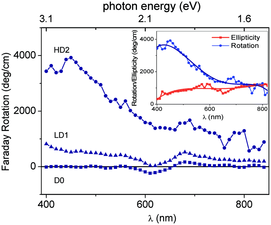 | ||
| Fig. 8 Room temperature Faraday rotation at 1.3 T for unirradiated D0, low (high) H-dose treated sample LD1 (HD2) treated films. Inset: Faraday rotation and ellipticity for the HD2 sample; lines are a guide to the eye. | ||
Finally, the efficiency of H-irradiation in producing large enhancements of ellipticity and FR in Zn1−xCoxO films may be exploited in many technological applications. In particular, it is possible to fabricate MO memories for information storage by combining H-irradiation with electron beam lithography deposition of H-opaque masks, with a fully controlled spatial modulation.27,28 The giant values of the FR may be indeed exploited for the fabrication of Faraday rotators, optical isolators1–3 and circulators taking advantage of the semiconducting nature of the Zn1−xCoxO which favours device integration. For this purpose, efforts are needed to improve the film microstructure which is generally responsible for high optical absorption loss leading to low values of the Faraday rotation over optical absorption coefficient ratio which undermines device performance.
4. Summary and conclusions
The irradiation of Zn1−xCoxO thin films with high doses of hydrogen ions induces a strong magneto-optical effect with a large enhancement in ellipticity and Faraday rotation at room temperature. Optical and microstructural analyses indicate that Co fully substitutes for Zn ions without noticeable Co-related secondary phases. The enhanced values of saturation magnetization, hysteretic ellipticity and Faraday rotation, confirm the intrinsic nature of the ferromagnetism arising from the interaction of magnetic ions and carriers in a partially filled donor-like band realized by the concurrent presence of Co-oxygen vacancies complexes and carriers.Based on recent theoretical and experimental results giving indications on the electronic states induced by Co-defect complexes in the ZnO energy gap, a phenomenological model is proposed which permits a thoroughly new, fine interpretation of the electronic transitions at the base of the ellipticity spectra.
Finally, the values of the Faraday rotation/ellipticity of the hydrogenated films in the visible range can be tuned by a suitable choice of the H dose and are promising in the perspective of non-reciprocal magneto-optical devices integrated on semiconductors and, generally speaking, for opto-spintronic devices.29
Conflicts of interest
There are no conflicts to declare.Acknowledgements
We are grateful to Enrico Patrizi and to Elvira Fantechi for their support with magnetic and magneto-optical measurements.References
- L. Bi, J. Hu, P. Jiang, H. S. Kim, D. H. Kim, M. C. Onbasli, G. F. Dionne and C. A. Ross, Magneto-Optical Thin Films for On-Chip Monolithic Integration of Non-Reciprocal Photonic Devices, Materials, 2013, 6, 5094–5117 CrossRef.
- Y. Shoji and T. Mizumoto, Magneto-optical non-reciprocal devices in silicon photonics, Sci. Technol. Adv. Mater., 2014, 15, 014602 CrossRef.
- M. Chandra Sekhar, M. R. Singh, S. Basu and S. Pinnepalli, Giant Faraday rotation in BixCe3-xFe5O12 epitaxial garnet film, Opt. Express, 2012, 20, 9624 CrossRef CAS.
- T. Goto, Y. Eto, K. Kobayashi, Y. Haga, M. Inoue and C. A. Ross, Vacuum annealed cerium-substituted yttrium iron garnet films on non-garnet substrates for integrated optical circuits, J. Appl. Phys., 2013, 113, 17A939 CrossRef.
- T. Okuda, N. Koshizuka, K. Hayashi, T. Takahashi, H. Kotani and H. Yamamoto, J. Magn. Soc. Jpn., 1987, 11(Suppl. S1), 179 Search PubMed.
- T. Boudiar, B. Payet-Gervy, M. F. Blanc-Mignon, J.-J. Rousseau, M. Le Berre and H. Joisten, Magneto-optical properties of yttrium iron garnet (YIG) thin films elaborated by radio frequency sputtering, J. Magn. Magn. Mater., 2004, 284, 77–85 CrossRef CAS.
- N. Kumar, S. Prasad, D. S. Misra, N. Venkataramani, M. Bohra and R. Krishnan, The influence of substrate temperature and annealing on the properties of pulsed laser-deposited YIG films on fused quartz substrate, J. Magn. Magn. Mater., 2008, 320, 2233–2236 CrossRef CAS.
- A. Di Trolio, P. Alippi, E. M. Bauer, G. Ciatto, M. H. Chu, G. Varvaro, A. Polimeni, M. Capizzi, M. Valentini, F. Bobba, C. Di Giorgio and A. Amore Bonapasta, Ferromagnetism and conductivity in hydrogen irradiated Co-doped ZnO thin films, ACS Appl. Mater. Interfaces, 2016, 8, 12925 CrossRef CAS.
- Y. C. Cho and S. J. Jeong, Reversible Ferromagnetic Spin Ordering Governed by Hydrogen in Co-doped ZnO Semiconductor, Appl. Phys. Lett., 2009, 95, 172514 CrossRef.
- Y. C. Cho and S. J. Jeong, Conductive and Ferromagnetic Contributions of H in ZnCoO Using H2 Hot Isostatic Pressure, Appl. Phys. Lett., 2012, 100, 112403 CrossRef.
- S. Lee, J. H. Park, B. S. Kim, D.-Y. Cho, Y. N. Choi, T.-W. Lee, W.-K. Kim, D. Kim, C. R. Cho, C. Moriyoshi, C. H. Park, Y. Kuroiwa and S.-Y. Jeong, Formation of ferromagnetic Co-H-Co complex and spin-polarized conduction band in Co-doped ZnO, Sci. Rep., 2017, 7, 11101 CrossRef.
- K. Ando and H. Saito, Large magneto-optical effect in an oxide diluted magnetic semiconductor Zn1−xCoxO, Appl. Phys. Lett., 2001, 78, 2700 CrossRef CAS.
- Z.-W. Jina, T. Fukumurab, K. Hasegawab, Y.-Z. Yooc, K. Andod, T. Sekiguchia, P. Ahmete, T. Chikyowa, T. Hasegawac, H. Koinumac and M. Kawasakib, Optical and electrical properties of Co-doped epitaxial ZnO films, J. Cryst. Grow., 2002, 237–239, 548–552 CrossRef.
- J. R. Neal, A. J. Behan, R. M. Ibrahim, H. J. Blythe, M. Ziese, A. M. Fox and G. A. Gehring, Room-temperature magneto-optics of ferromagnetic transition-metal-doped ZnO thin films, Phys. Rev. Lett., 2006, 19, 197208 CrossRef.
- K. R. Kittilsved, J. Zhao, W. K. Liu and J. D. Bryan, Magnetic circular dichroism of ferromagnetic Co2+-doped ZnO, Appl. Phys. Lett., 2006, 89, 062510 CrossRef.
- G. Campo, F. Pineider, V. Bonanni, M. Albino, A. Caneschi, C. De Julián Fernández, C. Innocenti and C. Sangregorio, A magneto-optical probe for the investigation of multiphase Fe oxide nanosystems, Chem. Mater., 2015, 27, 466–473 CrossRef CAS.
- S. Takeda and T. Kamino, Agglomeration of self-interstitials in Si observed at 450 °C by high-resolution transmission electron microscopy, Phys. Rev. B: Condens. Matter Mater. Phys., 1995, 2148, 51 Search PubMed.
- W. Zhou and H. F. Greer, What Can Electron Microscopy Tell Us Beyond Crystal Structures?, Eur. J. Inorg. Chem., 2016, 941–950 CrossRef CAS.
- S. Ramachandran, A. Tiwari and J. Narayan, Zn0.9Co0.1O-based diluted magnetic semiconducting thin films, Appl. Phys. Lett., 2004, 84, 5255 CrossRef CAS.
- P. Koidl, Optical absorption of Co2+ in ZnO, Phys. Rev. B: Condens. Matter Mater. Phys., 1977, 15, 2493 CrossRef CAS.
- C. D. Pemmaraju, R. Hanafin, T. Archer, H. B. Braun and S. Sanvito, Impurity-ion pair induced high-temperature ferromagnetism in Co-doped ZnO, Phys. Rev. B: Condens. Matter Mater. Phys., 2008, 7, 054428 CrossRef.
- G. Ciatto, A. Di Trolio, E. Fonda, P. Alippi, A. M. Testa and A. Amore Bonapasta, Evidence of Cobalt-Vacancy Complexes in Zn1−xCoxO Dilute Magnetic Semiconductors, Phys. Rev. Lett., 2011, 107, 127206 CrossRef CAS.
- A. Di Trolio, P. Alippi, G. Ciatto, G. Scavia, M. Valentini and A. Amore Bonapasta, The effect of Co doping on the conductive properties of ferromagnetic ZnxCo1-xO films, J. Mater. Chem. C, 2015, 3, 10188 RSC.
- K. R. Kittilsved, W. K. Liu and D. R. Gamelin, Electronic structure origins of polarity-dependent high-Tc ferromagnetism in oxide-diluted magnetic semiconductors, Nat. Mater., 2006, 5, 291 CrossRef.
- I. Abdolhosseini Sarsari, C. D. Pemmaraju, H. Salamati and S. Sanvito, Many-body quasiparticle spectrum of Co-doped ZnO: A GW perspective, Phys. Rev. B: Condens. Matter Mater. Phys., 2013, 87, 245118 CrossRef.
- D. D’Agostino, C. Di Giorgio, F. Bobba, A. Di Trolio, P. Alippi, A. M. Cucolo and A. Amore Bonapasta, Unexpected changes of ZnO surface reactivity and electronic structure induced by cobalt substitution, ACS Appl. Mater. Interfaces Search PubMed , under review.
- S. Birindelli, M. Felici, J. S. Wildmann, S. Johannes, A. Polimeni, M. Capizzi, A. Gerardino, S. Rubini, F. Martelli, A. Rastelli and R. Trotta, Single Photons on Demand from Novel Site-Controlled GaAsN/GaAsN:H Quantum Dots, Nano Lett., 2014, 14, 1275 CrossRef CAS.
- R. Trotta, A. Polimeni, F. Martelli, G. Pettinari, M. Capizzi, L. Felisari, S. Rubini, M. Francardi, A. Gerardino, P. Christianen and J. C. Maan, Fabrication of Site-Controlled Quantum Dots by Spatially Selective Incorporation of Hydrogen in Ga(AsN)/GaAs Heterostructures, Adv. Mater., 2011, 23, 2706–2710 CrossRef CAS.
- S.-H. Gong, F. Alpeggiani, B. Sciacca, E. C. Garnett and L. Kuipers, Nanoscale chiral valley-photon interface through optical spin-orbit coupling, Science, 2018, 359, 443 CrossRef CAS.
| This journal is © The Royal Society of Chemistry 2019 |