
 Open Access Article
 This Open Access Article is licensed under a
 Creative Commons Attribution 3.0 Unported Licence
Nanocrystalline Ga2O3 films deposited by spray pyrolysis from water-based solutions on glass and TCO substrates
Nina
Winkler
 *ab,
Rachmat Adhi
Wibowo
a,
Wolfgang
Kautek
b,
Giovanni
Ligorio
c,
Emil J. W.
List-Kratochvil
c and
Theodoros
Dimopoulos
*a
*ab,
Rachmat Adhi
Wibowo
a,
Wolfgang
Kautek
b,
Giovanni
Ligorio
c,
Emil J. W.
List-Kratochvil
c and
Theodoros
Dimopoulos
*a
aAIT Austrian Institute of Technology, Center for Energy, Photovoltaic Systems, Giefinggasse 6, A-1210 Vienna, Austria. E-mail: nina.winkler@ait.ac.at; theodoros.dimopoulos@ait.ac.at
bUniversity of Vienna, Department of Physical Chemistry, Währinger Straße 42, A-1090 Vienna, Austria
cHumboldt-Universität zu Berlin, Institut für Physik, Institut für Chemie, IRIS Adlershof, Brook-Taylor-Str. 6, 12489 Berlin, Germany
First published on 10th October 2018
Abstract
A low-cost and up-scalable fabrication method for high-quality gallium oxide films using spray pyrolysis from water-based solutions and moderate temperatures is presented. The solution chemistry and spraying process parameters were optimized to obtain homogeneous films on glass and three different transparent conducting oxide substrates. Structural and optical film properties of the deposited nanocrystalline Ga2O3 were evaluated by scanning electron microscopy, grazing-incidence X-ray diffraction, atomic force microscopy and optical spectroscopy. The elemental composition of the surface and the bulk film was analyzed by X-ray photoemission spectroscopy depth profiling. To show the applicability of the deposited Ga2O3 in electronic devices, the electronic valence region of the material was studied by ultraviolet photoemission spectroscopy, resulting in an energy level diagram of the material.
1 Introduction
Gallium oxide (Ga2O3), depending on the growth conditions and the crystal structure, is either an insulator or an n-type, wide-band gap semiconductor. There are several polymorphs of Ga2O3, but the most stable under ambient conditions, which has attracted the most attention, is monoclinic β-Ga2O3.1According to Varley et al.,2 the n-type conductivity of β-Ga2O3 originates from the unintentional incorporation of impurities during the deposition process rather than oxygen vacancies, which act solely as deep donors. An extensive review of Ga2O3 material properties, processing routes and devices was recently published by Pearton et al.,3 while β-Ga2O3, in particular, was reviewed by Park et al.4 The material has, indeed, found a wide range of applications in various disciplines. Single-crystals of Ga2O3 were synthesized by low-cost, melt growth techniques5 and were implemented in power electronic devices with high breakdown voltages, as replacements for the costly SiC and GaN.6 Thin layers of Ga2O3 have been applied in solar cells, for example as an ultrathin tunneling layer in dye-sensitized solar cells7 or as a passivation layer on silicon solar cells.8 Due to its low electron affinity, Ga2O3 was also successfully applied as an n-type buffer layer in Cu2O-type heterojunction solar cells.9,10 Due to its transparency in the deep UV spectral region, semiconducting β-Ga2O3 is especially attractive for solar-blind UV detectors11,12 or as a window layer in optoelectronic devices.13 Besides that, its high thermal (melting point 1715 °C)1 and chemical stability renders it applicable for sensors that operate under harsh conditions, such as reductive gas sensors.14 β-Ga2O3 can further be applied in water splitting devices, due to its photocatalytic properties.15
Gallium oxide films are often prepared by vacuum techniques, such as metal–organic chemical vapor deposition (MOCVD),16 molecular beam epitaxy (MBE),17 pulsed laser deposition (PLD)18 or atomic layer deposition (ALD).19 For lowering the processing costs, solution-based techniques are very attractive. Spray pyrolysis is a vacuum-free, easily up-scalable process, where the film deposition involves a precursor solution, sprayed in a carrier gas that is directed onto a heated substrate. For the droplet generation, there are various techniques available. Among them, ultrasonic agitation results in small droplet sizes (10–20 μm) with a uniform size distribution.20 Smaller solvent droplets are evaporated faster and the precursor salt decomposes before reaching the substrate surface, giving rise to film formation from the vapor phase.
This technique has already been applied for the deposition of Ga2O3 films,12,21–26 but most of the reported works have used toxic or flammable organic solvents like methanol24 and ethanol12,22 in the precursor solution. Avoiding organic solvents is highly desired, due to safety risks and environmental considerations, but using water-based solutions is a challenging task, demanding high deposition temperatures – above 400 °C – in order to achieve high-quality films.23,26 This is due to the high amount of heat that is required to evaporate water, because of the strong H–O–H hydrogen bonds and high boiling point.27 Further, no additional heat is transferred through exothermic burning, as compared to organic solvents. Another issue concerns the high surface tension of water, which leads to larger droplet sizes that require high evaporation temperatures.
Reports on using water-based solutions for the spray pyrolysis of Ga2O3 films at deposition temperatures below 400 °C are very limited,21,25 and they lack a comprehensive structural, electronic and chemical characterization of the deposited material.
This study explains for the first time how the chemistry of a water-based precursor solution and the spraying process parameters should be adjusted to obtain high-quality Ga2O3 films on bare glass and glass coated with different transparent conductive oxides (TCOs), while maintaining a moderate deposition temperature below 400 °C. Structural properties of the deposited Ga2O3 were analyzed in detail by scanning electron microscopy (SEM), atomic force microscopy (AFM) and grazing incidence X-ray diffraction (GIXRD). The chemical composition of the films on the surface and in the bulk was investigated by X-ray photoelectron spectroscopy (XPS). Optical properties of the material were examined by ultraviolet/visible/infrared (UV/Vis/IR) spectroscopy. To demonstrate the potential of the spray-deposited β-Ga2O3 in electronic devices, where a precise band alignment is crucial, ultraviolet photoelectron spectroscopy (UPS) spectra were recorded and an energy level diagram was constructed.
2 Experimental
2.1 Equipment
For the spray pyrolysis, a Sono-Tek ExactaCoat® system was used, equipped with a Sono-Tek Impact® ultrasonic nozzle in the horizontal geometry, operating at 120 kHz. The scanning speed of the nozzle over the substrate was 25 mm s−1 and the substrate to nozzle distance was 20 cm. All films were deposited using air as the carrier gas, with a pressure of 0.5 bar.The film thickness and morphology for each layer was evaluated by SEM (Zeiss Ultra 40) at an accelerating voltage of 5 kV. The surface topography was measured by AFM (Molecular Imaging, PicoPlus) in the tapping mode. The crystal structure was investigated by GIXRD (ThermoFisher Scientific ARL Equinox 100) at an angle of 1°, using Cu-Kα (λ = 1.5419 Å) radiation. Transmittance spectra in the range between 300 and 1100 nm were recorded by a Fourier transform infrared spectroscopy instrument (FTIR, Bruker Vertex 70), while in the range between 200 and 900 nm, they were recorded by a UV/Vis/IR spectroscopy instrument (Thermo Electron Corporation Nicolet evolution 100). XPS was measured in a JEOL JPS-9030 photoelectron spectrometer system using a monochromatic Al Kα (1486 eV) excitation source. XPS depth profiling was performed using an Ar+ ion source with 3 mA ion current and 300 V acceleration voltage. UPS spectra were measured using a hemispherical electron analyzer (Scienta SES 100) with a He I line exciton energy of 21.2 eV. The secondary electron cut-off (SECO) was measured with a bias voltage of −10 V. The energy position of the SECO and the low binding energy onset of emission of the highest occupied molecular level were determined through linear extrapolation of the peak half-maximum towards the background. The sheet-resistance was measured using a 4-point probe setup (Süss MicroTec probes) connected to a semiconductor parameter analyser (Agilent 4156 C).
2.2 Substrate preparation
Borosilicate glass substrates (Schott Nexterion® D, 7.5 × 2.5 cm2) and pure SiO2 substrates (Plan Optik, 2.5 × 2.5 cm2) were ultrasonically cleaned for 30 minutes at 50 °C in Hellmanex® III washing solution. The substrates were afterwards rinsed with deionized water (DI, 18 MΩ cm−1), isopropanol and dried in an air stream. Commercial tin-doped indium oxide (ITO, Sigma-Aldrich 703192, 8–12 Ω Sq−1) and fluorine-doped tin oxide (FTO, Sigma-Aldrich 735140-5EA, 5–7 Ω Sq−1) glass substrates were rinsed with isopropanol and dried in an air stream.Indium zinc oxide (IZO) substrates were prepared by spray pyrolysis on borosilicate substrates following a previously reported recipe.28 In brief, a precursor solution containing 0.2 M zinc acetate dihydrate (ZnAc2·2H2O, Sigma-Aldrich 96459), 4 mol% indium acetate (InAc3, Sigma-Aldrich 510270) and 8 vol% acetic acid (HAc, Sigma-Aldrich A6283) was used. Flow rate and temperature were set to 1.6 ml min−1 and 360 °C. A film thickness of 1.8 μm resulted in a sheet resistance of 20.7 Ω Sq−1 with an average transparency of 72% in the visible range between 450 and 700 nm.
2.3 Precursor solution preparation
For the optimized 0.04 M precursor solution, gallium acetylacetonate (Ga(acac)3) was dissolved in deionized water containing 3.5 M acetic acid. The solution was placed in an ultrasonic bath for 1 h at room temperature (25 °C) for complete dissolution of the precursor salt and was then directly used for the spray pyrolysis.3 Results and discussion
3.1 Spray pyrolysis of gallium oxide
| Reaction | log![[thin space (1/6-em)]](https://www.rsc.org/images/entities/char_2009.gif) β (25 °C) β (25 °C) |
Ref. |
|---|---|---|
| H2O ↔ H+ + OH− | −13.73 | 33 |
| Ga3+ + H2O ↔ [Ga(OH)]2+ + H+ | −3.73 | 31 |
| Ga3+ + 2H2O ↔ [Ga(OH)2]+ + 2H+ | −7.15 | 31 |
| Ga3+ + 3H2O ↔ [Ga(OH)3]0 + 3H+ | −8.20 | 32 |
| Ga3+ + 4H2O ↔ [Ga(OH)4]− + 4H+ | −17.30 | 32 |
| HAc ↔ H+ + Ac− | −4.49 | 33 |
| Ga3+ + HAc ↔ [GaAc]2+ + H+ | −2.08 | 33 |
| 2Ga3+ + HAc + 2H2O ↔ [Ga2(OH)2Ac]3+ + 3H+ | −5.65 | 33 |
| Ga3+ + Acac− ↔ [Ga(acac)]2+ | 23.65 | 34 |
| Ga3+ + 2Acac− ↔ [Ga(acac)2]+ | 17.27 | 34 |
| Ga3+ + 3Acac− ↔ [Ga(acac)3]0 | 9.29 | 34 |
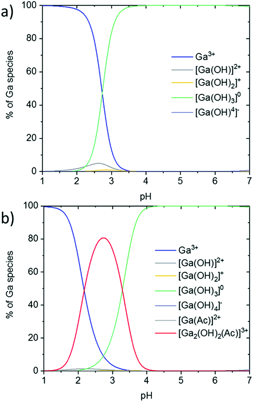 | ||
| Fig. 1 Ga speciation without acetylacetonate ligands (a) in pure water and (b) in water + 3.5 M HAc. | ||
To stabilize Ga3+ in acidic aqueous solutions and avoid Ga(OH)3 precipitation, complexation with chelate ligands results in thermodynamically stable gallium complexes.35 In spray pyrolysis, Ga3+ is often stabilized by acetylacetonate ligands, due to the volatile properties of the complex for a CVD-like film growth.36,37 Further, gallium acetylacetonate (Ga(acac)3) is commercially available and a low-cost gallium precursor compound. A disadvantage of (Ga(acac)3) is its low solubility in aqueous solutions.
Despite the fact that Ga(acac)3 is a very stable complex (see also the complex stability constants in Table 1), the ligands can be replaced by hydroxide ions in water-based solutions, as proposed in the literature.23,38 For this reason, acetic acid was added to additionally stabilize the Ga3+ ions in the solution by acetate–hydroxide complexes, as displayed in the speciation diagram in Fig. 1(b).
| Ga(acac)3 (M) | Acetic acid (M) | pH value | Surface tension (mN m−1) | Solution density (g ml−1) | Droplet size (μm) |
|---|---|---|---|---|---|
| 0.02 | 0.35 | 3.50 | 71.5 | 1.002 | 16.98 |
| 0.02 | 3.50 | 2.41 | 60.5 | 1.025 | 16.06 |
| 0.03 | 3.50 | 2.55 | 60.5 | 1.025 | 16.06 |
| 0.04 | 3.50 | 2.61 | 60.5 | 1.025 | 16.06 |
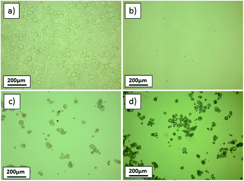 | ||
| Fig. 2 Microscope images of sprayed Ga2O3 films on glass, obtained from the following solution compositions: (a) 0.02 M Ga(acac)3 + 0.35 M HAc, (b) 0.02 M Ga(acac)3 + 3.50 M HAc, (c) 0.03 M Ga(acac)3 + 3.50 M HAc, and (d) 0.04 M Ga(acac)3 + 3.50 M HAc. | ||
The addition of acetic acid not only changes the Ga-species distribution, but it also decreases the surface tension γ of the solvent, resulting in a smaller droplet size. The mean droplet size generated by ultrasonic spray pyrolysis is given by Lang's equation:20
 | (1) |
For higher Ga(acac)3 concentrations and a nearly constant pH value, some precipitates were seen on the glass slides (Fig. 2(c) and (d)), which are most likely residues from incomplete decomposition of metal salts before reaching the hot substrate.
To maintain a reasonable growth rate of ∼1 nm min−1 and minimize the processing time, the solution composition of 0.04 M Ga(acac)3 and 3.5 M acetic acid was used, and the unwanted precipitates were avoided through adjustment of equipment parameters. The critical parameter in ultrasonic spray pyrolysis is the temperature, since it is involved in all important processes such as aerosol transport, solvent evaporation and precursor decomposition. As the deposition temperature was increased from 360 °C (used in the previous experiments) to 380 and 400 °C (Fig. 3(a) and (b)), the precipitates disappeared.
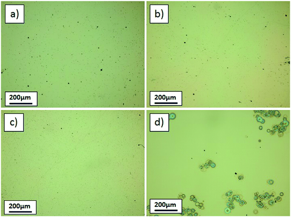 | ||
| Fig. 3 Microscope images of sprayed Ga2O3 films deposited at the following temperature and flow rate values: (a) 380 °C and 0.8 ml min−1, (b) 400 °C and 0.8 ml min−1, (c) 380 °C and 1.2 ml min−1, and (d) 380 °C and 1.6 ml min−1. | ||
To further accelerate the deposition and avoid substrate cooling during the process, the number of spraying cycles that yield the targeted film thickness must be minimized. This can be achieved by increasing the solution flow rate. The local temperature and the flow rate are inevitably connected, because a higher flow rate results in an increased substrate cooling with each spraying cycle. As the flow rate increased from 0.8 ml min−1 to 1.6 ml min−1, precipitates start to appear again (see microscope image in Fig. 3(d)). Setting the flow rate at 1.2 ml min−1 and the temperature at 380 °C, a high-quality Ga2O3 film was obtained (Fig. 3(c)), and these parameters were defined as the standard conditions for all subsequent depositions on all substrates.
3.2 Ga2O3 film characterization on glass and TCO substrates
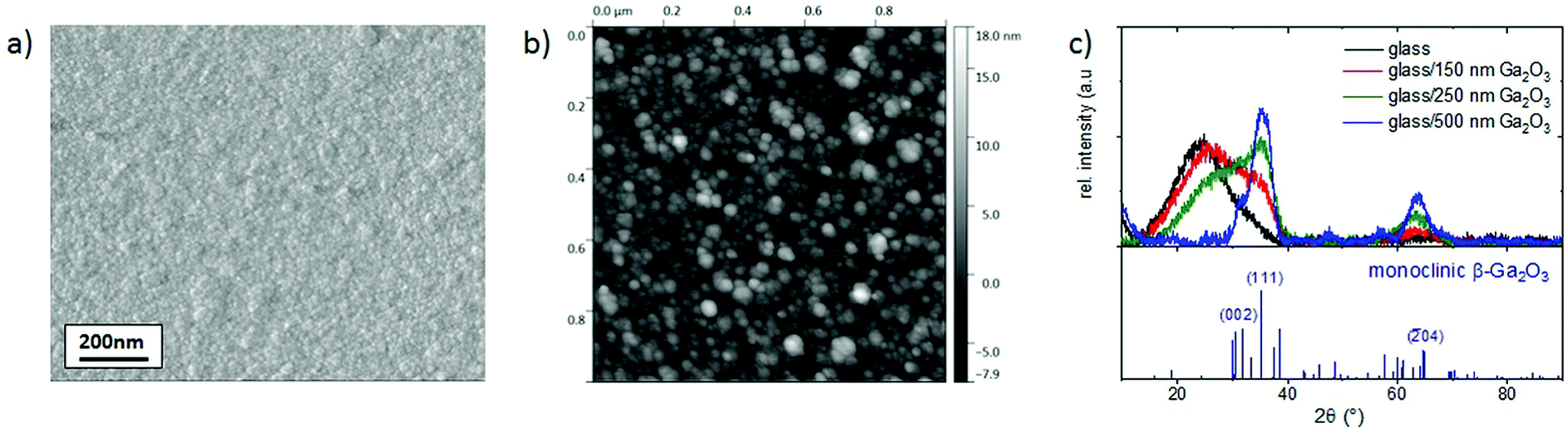 | ||
| Fig. 4 Ga2O3 film (150 nm) deposited on borosilicate glass: (a) SEM image, (b) AFM image and (c) GIXRD (1°) including the monoclinic β-Ga2O3 reference pattern. | ||
To study the crystal structure of the Ga2O3 film, GIXRD diffractograms were recorded (Fig. 4(c)). As discussed before, the crystal structure of Ga2O3 depends on the growth method and conditions. Ga2O3 films deposited by spray pyrolysis are mostly amorphous21,23,24,26 or nanocrystalline.22 Monoclinic β-Ga2O3 was only reported for much higher processing temperatures (>800 °C)12 or by including an additional annealing step (>700 °C).21,23,24 The films in this study (Fig. 4(c)) show two broad reflections in the range of the monoclinic β-Ga2O3 phase (COD 96-200-4988) and a broad background peak for the amorphous glass substrate. The first reflection can be assigned to the (111) β-Ga2O3 plane, while the second one cannot be assigned to a specific plane for 150 nm Ga2O3 films, due to the many possible plane reflections for the broad peak at ∼64°. For thicker films, the peak intensity increases and the reflection can be assigned to a specific plane. The broadness and weakness of the reflections support a film growth with crystallite sizes in the nm range. To minimize the intensity of the amorphous glass substrate peak in the XRD pattern, Ga2O3 films with ∼250 and 500 nm thickness (1100 and 2200 spraying cycles) were deposited. With increasing film thickness, the (002) and (111) reflections, attributed to monoclinic β-Ga2O3, become more prominent. Additionally, the broad reflection around 64° can be assigned to the (![[2 with combining macron]](https://www.rsc.org/images/entities/char_0032_0304.gif) 04) β-Ga2O3 plane. The (111) and (04) reflections were used to calculate the crystallite size by the Scherrer formula,41 yielding 2.48 and 2.36 nm, respectively. In conclusion, although other phases cannot be excluded, taking into account the relative stabilities of the possible phases and the peak positions, the monoclinic β-Ga2O3 phase predominates (as is more clearly demonstrated for thicker films), albeit with nanosized crystallites.
04) β-Ga2O3 plane. The (111) and (04) reflections were used to calculate the crystallite size by the Scherrer formula,41 yielding 2.48 and 2.36 nm, respectively. In conclusion, although other phases cannot be excluded, taking into account the relative stabilities of the possible phases and the peak positions, the monoclinic β-Ga2O3 phase predominates (as is more clearly demonstrated for thicker films), albeit with nanosized crystallites.
To investigate the influence of different substrates on the Ga2O3 film morphology, films were deposited on sprayed IZO, commercial ITO and FTO substrates. For many devices, such as in buffer layers in photovoltaics, Ga2O3 needs to be deposited on a TCO substrate. SEM pictures of the substrates with and without the Ga2O3 film are displayed in Fig. 5(a)–(f). It was observed that the Ga2O3 film morphology and grain size were not affected by the TCO substrate. Pinhole-free Ga2O3 grew homogenously, independent from the underlying TCO morphology. Small grain sizes between 10 and 20 nm were formed on IZO, ITO and FTO. On FTO, the large grains of the underlying substrate are still visible, but all of them are completely covered by Ga2O3. To further test that the film is hole-free, we drew macroscopic contacts (∼4 mm2 in area), using water-based conductive carbon paste, on the top of the Ga2O3 (20 nm thick). A bottom contact was also drawn on the TCO. We then measured the resistance between the bottom and top contacts, which was found to be in the region of 10 MΩ in the case of IZO and even larger for ITO.
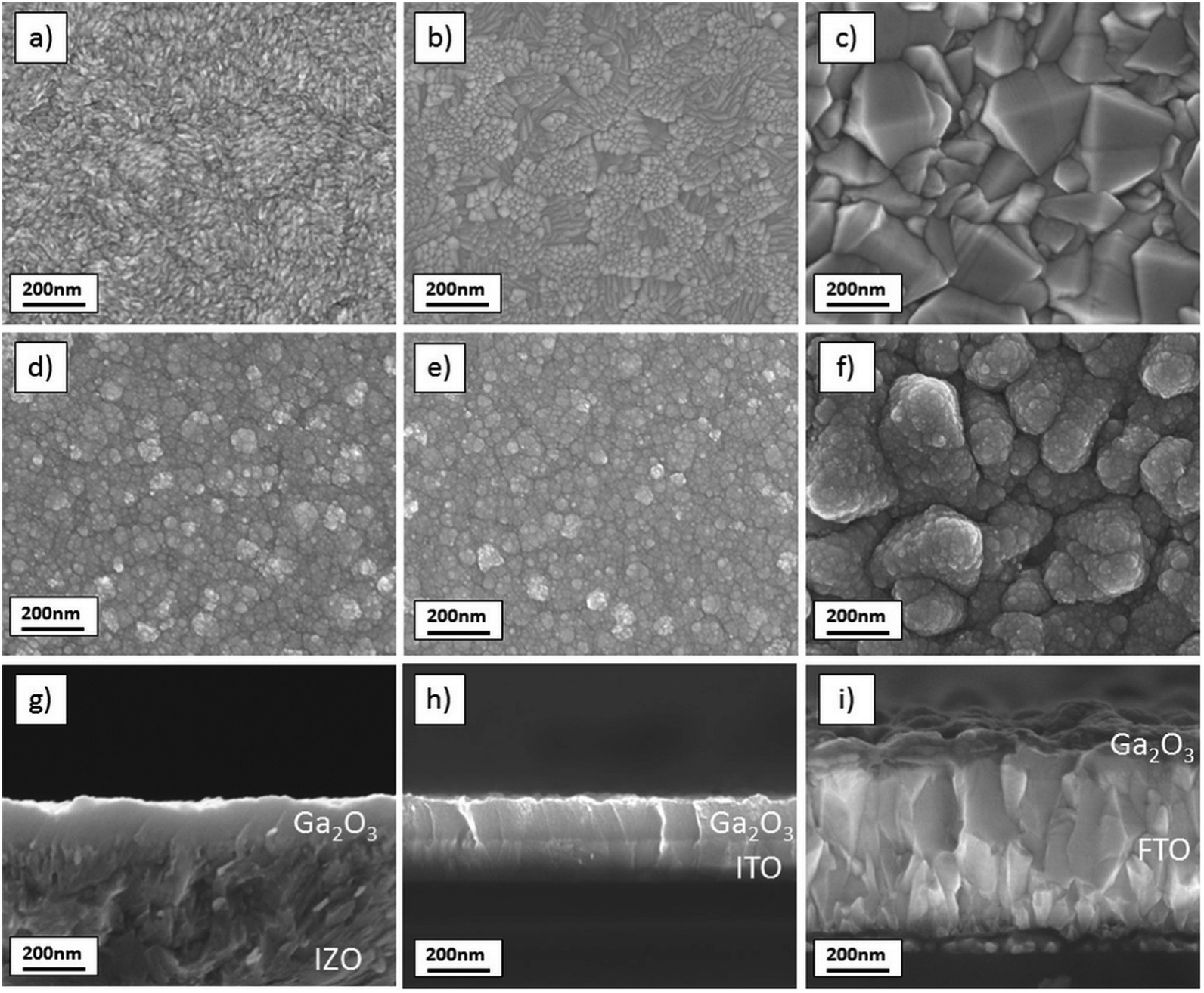 | ||
| Fig. 5 SEM plane views of (a) IZO substrate, (b) ITO substrate, (c) FTO substrate, (d) IZO/Ga2O3, (e) ITO/Ga2O3, (f) FTO/Ga2O3 and cross sections of (g) IZO/Ga2O3, (h) ITO/Ga2O3, and (i) FTO/Ga2O3. | ||
SEM cross sections reveal the film growth in more detail (Fig. 5(g)–(i)). It appears that the Ga2O3 grows homogeneously as a nanocrystalline film on all substrates. The film thickness of 150 nm is independent of the substrate, which suggests a similar heat conductivity of all three TCOs, since temperature is one of the critical factors determining the film growth rate.
To investigate the crystal structure of Ga2O3 on the various substrates, GIXRD diffractograms at 1° were recorded (Fig. 6(a)–(c)). On IZO, FTO and ITO substrates, no broad (111) β-Ga2O3 peak can be distinguished, because the (101) hexagonal zinc(II) oxide, the (101) tetragonal tin(IV) oxide and the (400) cubic indium(III) oxide reflections are located at the same 2θ angle. In combination with the SEM pictures, it appears that the underlying TCO does not influence the growth of the Ga2O3 film.
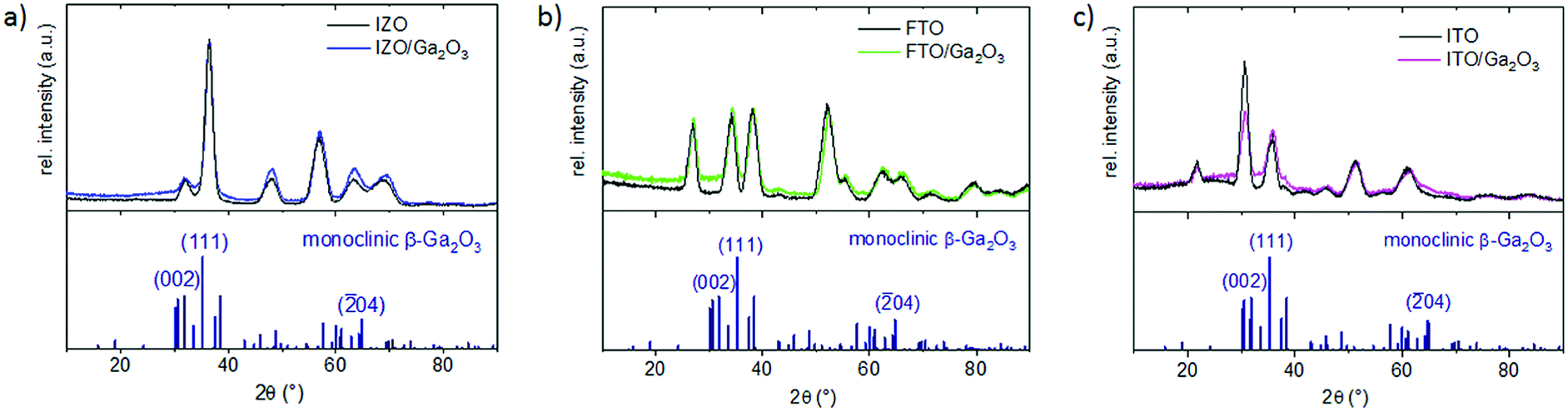 | ||
| Fig. 6 XRD diffractograms of Ga2O3 films on TCO substrates including the monoclinic β-Ga2O3 reference pattern (a) on IZO, (b) on FTO, and (c) on ITO. | ||
Since the deposition of Ga2O3 on TCO substrates is a relevant step for device fabrication, like in photovoltaic cells, the sheet resistance of the three different TCOs after Ga2O3 deposition at 380 °C was measured. It was seen that for all three substrates, the deposition of 30 nm Ga2O3 (a usual buffer layer thickness in photovoltaic cells) did not modify the sheet resistance of the underlying TCO. The sheet resistance of IZO after the Ga2O3 deposition was 22.0 Ω Sq−1, 5.8 Ω Sq−1 for FTO and 9.7 Ω Sq−1 for ITO. This shows that the used deposition conditions do not affect the conductivity of TCO, and they can therefore be applied on electrodes for device fabrication.
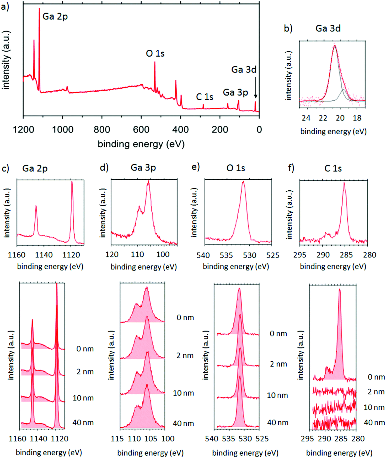 | ||
| Fig. 7 (a) XPS analysis of Ga2O3 with (b) Ga 3d, (c) Ga 2p, (d) Ga 3p, (e) O 1s and (f) C 1s core levels including XPS depth profiling. | ||
Fig. 7(c)–(f) shows that the signal shape does not change depending on the depth, hence indicating the same chemical environment throughout the entire film. The signal ratio Ga/O was calculated from the corresponding XPS signals to determine the film stoichiometry as a function of the depth. Table 3 shows that a ratio of about 50%:50% for Ga 2p:O 1s and Ga 3p:O 1s could be observed, indicating that the film is Ga-rich, suggesting the presence of two Gallium oxidation states, namely Ga(I)oxide (Ga2O) and Ga(III)oxide (Ga2O3). The Ga 3d core level, displayed in Fig. 7(b) can be used to identify the ratio between Ga(I) (peak at 19.6 eV in binding energy) and Ga(III) (at 20.6 eV).42 The peak area gives a ratio of Ga(III):Ga(I) of 85%:15%. Ga2O3 is composed of 40% Ga(III) and 60% O and Ga2O is composed of 66.7% Ga(I) and 33.3% O. Since 15% Ga(I) and 85% Ga(III) are present, this gives a signal ratio of Ga:O of 44%:56%, which is in agreement with the ratio measured by XPS.
| Depth (nm) | Ga 2p (%) | O 1s (%) | Ga 3p (%) | O 1s (%) |
|---|---|---|---|---|
| 0 | 30.23 | 69.77 | 45.97 | 54.03 |
| 1 | 46.9 | 53.1 | 50.7 | 49.3 |
| 2 | 48.39 | 51.61 | 51.96 | 48.04 |
| 5 | 49.12 | 50.88 | 52.14 | 47.86 |
| 10 | 48.95 | 51.05 | 51.85 | 48.15 |
| 40 | 49.28 | 50.72 | 52.22 | 47.78 |
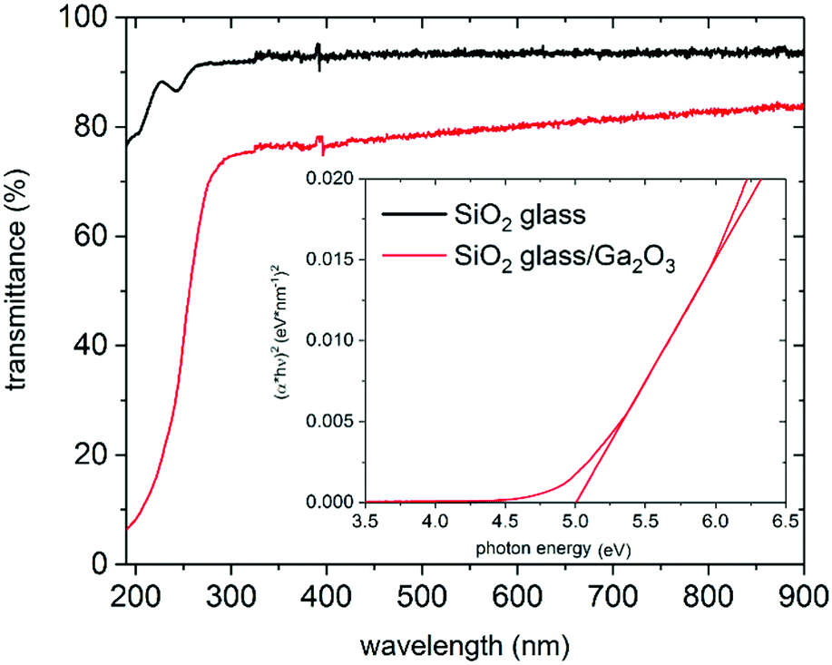 | ||
| Fig. 8 Transmittance of Ga2O3 on pure SiO2 glass (inset shows the band gap). | ||
The transparency of the films on SiO2 substrates between 300 and 900 nm is above 70%, and on borosilicate glass, it is above 80% (see Fig. 8 and 9(a)). The thicker Ga2O3 film (250 nm) in Fig. 9(a) shows Fabry–Perot interferences, which are commonly observed in dense films. Ga2O3 films on TCO substrates (Fig. 9(b)–(d)) do not cause a change in transparency of the native substrate. On ITO substrates, the transparency in the UV region can be slightly improved through the Ga2O3 layer, which is probably caused by the effect of the elevated deposition temperature on the ITO film.
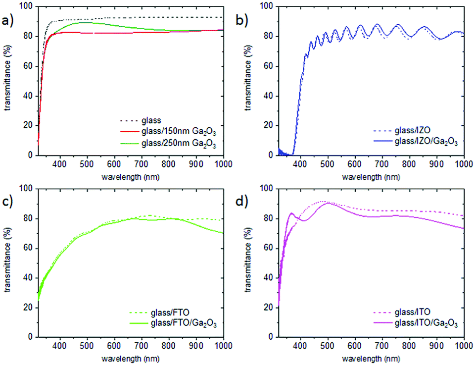 | ||
| Fig. 9 Transmittance of Ga2O3 on various substrates: (a) borosilicate glass, (b) IZO, (c) FTO, and (d) ITO. | ||
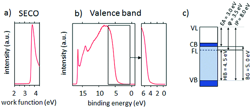 | ||
| Fig. 10 UPS measurements of Ga2O3 (a) SECO, (b) valence band survey and (c) energy diagram. | ||
4 Conclusion
In this study, we have shown how the composition of water-based solutions and spray pyrolysis processing parameters have to be adjusted for the deposition of high-quality Ga2O3 films at temperatures below 400 °C. Structural film properties were studied by GIXRD, AFM and SEM showing that the material is nanocrystalline (∼2.4 nm grain size) with broad peaks that can be assigned to β-Ga2O3 and low surface roughness. XPS depth profiling revealed that the film is Ga-rich with Ga(III):Ga(I) in an 85%:15% ratio. The work function, the electron affinity and the ionization potential of the spray deposited films were determined as 3.5, 3.0 and 8.0 eV. In order to demonstrate that Ga2O3 can be implemented in devices, homogeneous films were deposited on three different TCO substrates (IZO, ITO and FTO) without compromising the TCO sheet resistance and transparency.
Conflicts of interest
There are no conflicts of interest to declare.Acknowledgements
We would like to thank Stefan Edinger and Lukas Kinner for fruitful discussions.References
- R. Roy, V. G. Hill and E. F. Osborn, J. Am. Chem. Soc., 1952, 74, 719–722 CrossRef CAS.
- J. B. Varley, J. R. Weber, A. Janotti and C. G. Van de Walle, Appl. Phys. Lett., 2010, 97, 142106 CrossRef.
- S. J. Pearton, J. Yang, P. H. Cary, F. Ren, J. Kim, M. J. Tadjer and M. A. Mastro, Appl. Phys. Rev., 2018, 5, 11301 Search PubMed.
- J.-H. Park, R. McClintock, D. Pavlidis, F. H. Teherani, D. J. Rogers, B. A. Magill, G. A. Khodaparast, Y. Xu, J. Wu, V. P. Dravid and M. Razeghi, in Oxide-based Materials and Devices IX, International Society for Optics and Photonics, 2018, vol. 10533, p. 105330R Search PubMed.
- E. Ohba, T. Kobayashi, M. Kado and K. Hoshikawa, Jpn. J. Appl. Phys., 2016, 55, 1202BF CrossRef.
- M. Higashiwaki, K. Sasaki, H. Murakami, Y. Kumagai, A. Koukitu, A. Kuramata, T. Masui and S. Yamakoshi, Semicond. Sci. Technol., 2016, 31, 34001 CrossRef.
- A. K. Chandiran, N. Tetreault, R. Humphry-Baker, F. Kessler, E. Baranoff, C. Yi, M. K. Nazeeruddin and M. Grätzel, Nano Lett., 2012, 12, 3941–3947 CrossRef CAS.
- T. G. Allen and A. Cuevas, Phys. Status Solidi RRL, 2015, 9, 220–224 CrossRef CAS.
- T. Minami, Y. Nishi and T. Miyata, Appl. Phys. Express, 2013, 6, 44101 CrossRef.
- Y. S. Lee, D. Chua, R. E. Brandt, S. C. Siah, J. V. Li, J. P. Mailoa, S. W. Lee, R. G. Gordon and T. Buonassisi, Adv. Mater., 2014, 26, 4704–4710 CrossRef CAS.
- T. Oshima, T. Okuno, N. Arai, N. Suzuki, S. Ohira and S. Fujita, Appl. Phys. Express, 2008, 1, 11202 CrossRef.
- Z. Ji, J. Du, J. Fan and W. Wang, Opt. Mater., 2006, 28, 415–417 CrossRef CAS.
- Y. Tomm, J. M. Ko, A. Yoshikawa and T. Fukuda, Sol. Energy Mater. Sol. Cells, 2001, 66, 369–374 CrossRef CAS.
- M. Fleischer, L. Höllbauer and H. Meixner, Sens. Actuators, B, 1994, 18, 119–124 CrossRef CAS.
- S. Jin, X. Wang, X. Wang, M. Ju, S. Shen, W. Liang, Y. Zhao, Z. Feng, H. Y. Playford, R. I. Walton and C. Li, J. Phys. Chem. C, 2015, 119, 18221–18228 CrossRef CAS.
- Y. Lv, J. Ma, W. Mi, C. Luan, Z. Zhu and H. Xiao, Vacuum, 2012, 86, 1850–1854 CrossRef CAS.
- D. Guo, Z. Wu, P. Li, Y. An, H. Liu, X. Guo, H. Yan, G. Wang, C. Sun, L. Li and W. Tang, Opt. Mater. Express, 2014, 4, 1067–1076 CrossRef.
- Q. Feng, F. Li, B. Dai, Z. Jia, W. Xie, T. Xu, X. Lu, X. Tao, J. Zhang and Y. Hao, Appl. Surf. Sci., 2015, 359, 847–852 CrossRef CAS.
- D. Choi, K.-B. Chung and J.-S. Park, Thin Solid Films, 2013, 546, 31–34 CrossRef CAS.
- R. Rajan and A. B. Pandit, Ultrasonics, 2001, 39, 235–255 CrossRef CAS.
- R. Pandeeswari and B. G. Jeyaprakash, Sens. Actuators, B, 2014, 195, 206–214 CrossRef CAS.
- S. R. Thomas, G. Adamopoulos, Y.-H. Lin, H. Faber, L. Sygellou, E. Stratakis, N. Pliatsikas, P. A. Patsalas and T. D. Anthopoulos, Appl. Phys. Lett., 2014, 105, 92105 CrossRef.
- P. Wu, Y.-M. Gao, R. Kershaw, K. Dwight and A. Wold, Mater. Res. Bull., 1990, 25, 357–363 CrossRef CAS.
- A. Ortiz, J. C. Alonso, E. Andrade and C. Urbiola, J. Electrochem. Soc., 2001, 148, F26–F29 CrossRef CAS.
- H. Kim and W. Kim, J. Appl. Phys., 1987, 62, 2000–2002 CrossRef CAS.
- J. Hao and M. Cocivera, J. Phys. D: Appl. Phys., 2002, 35, 433 CrossRef CAS.
- E. Arca, K. Fleischer and I. V. Shvets, J. Phys. Chem. C, 2009, 113, 21074–21081 CrossRef CAS.
- N. Winkler, S. Edinger, J. Kaur, R. A. Wibowo, W. Kautek and T. Dimopoulos, J. Mater. Sci., 2018, 53, 12231–12243 CrossRef CAS.
- S. A. Wood and I. M. Samson, Ore Geol. Rev., 2006, 28, 57–102 CrossRef.
- Aqueous solutions, http://www.acadsoft.co.uk/aq_solutions.htm, accessed July 9, 2018.
- P. L. Brown, J. Chem. Soc., Dalton Trans., 1989, 399–402 RSC.
- I. Tóth, L. Zékány and E. Brücher, Polyhedron, 1984, 3, 871–877 CrossRef.
- M. Clausén, L.-O. Öhman, J. D. Kubicki and P. Persson, J. Chem. Soc., Dalton Trans., 2002, 2559–2564 RSC.
- J. Stary and J. O. Liljenzin, Pure Appl. Chem., 2009, 54, 2557–2592 Search PubMed.
- W. R. Harris and A. E. Martell, Inorg. Chem., 1976, 15, 713–720 CrossRef CAS.
- J. C. Viguié and J. Spitz, J. Electrochem. Soc., 1975, 122, 585–588 CrossRef.
- P. Marchand and C. J. Carmalt, Coord. Chem. Rev., 2013, 257, 3202–3221 CrossRef CAS.
- W. J. DeSisto, Y.-T. Qian, C. Hannigan, J. O. Edwards, R. Kershaw, K. Dwight and A. Wold, Mater. Res. Bull., 1990, 25, 183–189 CrossRef CAS.
- E. Álvarez, G. Vázquez, M. Sánchez-Vilas, B. Sanjurjo and J. M. Navaza, Surface Tension of Organic Acids + Water Binary Mixtures from 20 °C to 50 °C, https://pubs.acs.org/doi/abs/10.1021/je970025m, accessed July 11, 2018.
- Density of aqueous solutions of organic acids, https://www.engineeringtoolbox.com/density-aqueous-solution-formic-lactic-oxalic-acetic-citric-acid-concentration-d_1953.html, accessed July 11, 2018.
- A. L. Patterson, Phys. Rev., 1939, 56, 978–982 CrossRef CAS.
- R. Carli and C. L. Bianchi, Appl. Surf. Sci., 1994, 74, 99–102 CrossRef CAS.
- J. Tauc, Mater. Res. Bull., 1968, 3, 37–46 CrossRef CAS.
| This journal is © The Royal Society of Chemistry 2019 |