
Liquid thin film dewetting-driven micropatterning of reduced graphene oxide electrodes for high performance OFETs†
Sung Min
Lee‡
a,
Seung Keun
Song‡
a,
Seongwon
Yoon
b,
Dae Sung
Chung
 *b and
Suk Tai
Chang
*a
*b and
Suk Tai
Chang
*a
aSchool of Chemical Engineering and Materials Science, Chung-Ang University, Seoul 06974, Republic of Korea. E-mail: stchang@cau.ac.kr
bDepartment of Energy Science and Engineering, Daegu Gyeongbuk Institute of Science and Technology (DGIST), Daegu 42988, Republic of Korea. E-mail: dchung@dgist.ac.kr
First published on 27th November 2018
Abstract
We present a novel approach to produce high-resolution reduced graphene oxide (rGO) micropatterns based on a dewetting phenomenon of liquid thin films. The uniform liquid thin film of aqueous graphene oxide (GO) dispersion was formed by the meniscus dragging deposition method on a pre-patterned silanized substrate. Subsequently, selective dewetting of the water layer was induced due to the surface energy gradient on the coating substrates. After drying and chemical reduction, the high-resolution rGO micropatterns with a minimum feature size of 10 μm were realized over a large area substrate by consuming less than 1 μL of GO solution per square centimeter. As a demonstration of the application of this patterning technique, we have successfully fabricated organic field-effect transistors (OFETs) based on rGO pattern arrays as source–drain electrodes. The OFETs with the rGO electrodes exhibited a field effect mobility of 0.6 cm2 (V s)−1 with an on/off ratio of 1.79 × 10⁶, which is higher than that of the devices with Au source–drain contacts.
Introduction
Graphene—a two-dimensional carbon lattice—has excellent electrical conductivity, optical transmittance, and flexibility.1,2 Graphene with these properties could be utilized in opto-electronic devices,3–6 sensors,7–14 and energy devices.15–17 Graphene is usually synthesized by chemical vapor deposition (CVD), liquid-phase physical exfoliation, or chemical exfoliation–reduction.18,19 Graphene produced by CVD has the most sophisticated structure and has excellent physical properties. However, it has high production cost and low yield.20 Thus, CVD-synthesized graphene is mainly used for fundamental research and ultra-precision devices that do not require mass production. Liquid-phase physical exfoliation, typically assisted by ultra-sonication, produces high-quality liquid-dispersed graphene. However, a surfactant is required to make graphene disperse well in a solvent. The graphene obtained also tends to be highly poly-dispersed.21 Therefore, the removal of the surfactant and the filtration process for flake size selection remain challenges to reliable mass production. On the other hand, chemical exfoliation (as in Hummer's method) produces graphene oxide (GO), which is used as a precursor to graphene. GO can be easily reduced by chemical, thermal, or photo-chemical methods. The sp2-hybridized carbon network can be recovered by reduction and improved electrical conductivity.22,23 The reduced graphene oxide (rGO) has a defective structure resulting from imperfect reduction, which causes resistance increase. However, it still has excellent electrical conductivity, flexibility, and optical transparency. Enabling the solution process and lowering the manufacturing cost help commercialization. Therefore, rGO has received attention as a source of graphene for application in future opto-electronic devices.24To utilize rGO in opto-electronic devices, a high-resolution patterning technique should be followed. Thus, much effort has been devoted to implanting elaborate rGO patterns. Particularly, ink-jet printing, soft lithography, and partial area reduction of GO by UV-irradiation have been applied to produce the rGO patterns. Ink-jet printing is considered the promising patterning technique due to its additive printing ability, low cost of operation, and scalability. However, difficulty in ink preparation and relatively low resolution of patterns are still challenging. For efficient ink-jet printing, high viscosity is required for the ink, while most solvents having good printing abilities have low viscosities.25 The concentration of GO is often lower than 0.01%, thus requiring multiple iterations of ink-jet printing.26 The toxicity of solvents is another problem. For instance, N-methyl-2-pyrrolidone (NMP) used in the ink-jet printing of GO flakes is rapidly absorbed by inhalation and disturbs human organisms. Some studies have reported water-based ink-jet printed rGO patterns to eliminate ink toxicity. However, low resolution and the coffee ring effect pose obstacles to achieving high quality patterning.27 Soft lithography can fabricate rGO patterns with high resolution. The pre-designed soft mold can peel off the designed area, retaining the rGO patterns.28 The pattern is obtained by tearing off from the original thin film and a well-defined edge shape is rarely obtained; and it retains a tear mark.29–31 The patterning process is cumbersome, and it is difficult to achieve a pattern multiple times with a single mold. As an alternative approach, the method of partial reduction using UV-irradiation has been used to produce rGO patterns. However, it requires a long irradiation time from 1 h to 24 h and the unwanted GO region remains wherever UV is not irradiated.32–34 Therefore, an innovative patterning method is required to fully exploit the advantages of chemically exfoliated graphene oxides.
Here, we report a new approach to fabricate high-resolution and uniform rGO patterns using dewetting phenomena in liquid thin films. The surface energy of a coating substrate was adjusted by pre-patterning trichloro(octadecyl)silane (ODTS) to induce selective dewetting of water thin film containing GO flakes on the substrate. The meniscus dragging deposition (MDD) technique, previously reported by our group,35 was used to form uniform liquid thin films on the ODTS-prepatterned substrate. The water thin film was dewetted due to the surface energy gradient on the ODTS-prepatterned substrate. After drying and chemical reduction, the rGO micropatterns were implanted over the substrate with a minimum feature size of 10 μm. Various shaped rGO patterns were also realized over a large area substrate using less than 1 μL of aqueous GO solution per square centimeter. Although the patterning of conducting polymers, silver nanowires, and carbon nanotubes was realized by using the dewetting phenomenon,36–38 those methods are limited to the fabrication of simple square or line patterns. The validity of our rGO patterning method to source–drain electrodes of OFETs was also investigated. The OFETs that used our rGO electrode patterns exhibited two orders of magnitude higher on/off ratio and two times higher hole mobility compared to OFETs with conventional thermally deposited Au electrodes.
Experimental
Preparation of selectively hydrophilized substrates
Substrates such as glass slides (25 mm × 75 mm with plain ends, Fisher Scientific, USA) and Si/SiO2 wafers (Namkang Hi-Tech Co., Korea) were cleaned with piranha solution. The cleaned substrates were dried with an air blower and hydrophilized by an air plasma treatment (PDC-32G, Harrick Plasma) at high power (18 W) for 3 min. The hydrophilized substrates were soaked in a toluene bath mixed with 0.2 vol% trichloro(octadecyl)silane (ODTS, Sigma Aldrich) for 20 min and then rinsed with toluene and dried by blowing air. The ODTS-treated substrates were attached with a quartz chrome mask containing pattern designs and exposed to 185 nm and 250 nm UV light for 20 min (Ozone cure 16, Minuta technology Co.).Fabrication of rGO patterns
A few microliters of graphene oxide solution (SKU-HCGO-W-175, Graphene supermarket) were injected between a hydrophilized deposition plate and a pretreated substrate. The trapped liquid meniscus was dragged onto the selectively hydrophilized surface by one-way linear motion of the hydrophilized deposition plate attached to a motorized stage (AL1-1515-3S, Micro Motion Technology, Valley Center, USA) and dried at room temperature. The dried GO pattern was heated in a crystallizing dish with 200 μL reducing agent (HI![[thin space (1/6-em)]](https://www.rsc.org/images/entities/char_2009.gif) :acetic acid = 2:5 volume ratio mixed) at 80 °C for 30 min. The reduced GO patterns were soaked in DI water for 5 min and dried on a hotplate at 80 °C.
:acetic acid = 2:5 volume ratio mixed) at 80 °C for 30 min. The reduced GO patterns were soaked in DI water for 5 min and dried on a hotplate at 80 °C.
Characterization of rGO patterns
The images of rGO patterns were taken using an optical microscope (Olympus BX-51) and a scanning electron microscope (Carl Zeiss SIGMA FE-SEM). The topographies and thicknesses of the patterns were characterized by atomic force microscopy (AFM, NX-10, Park systems) in a non-contact mode. Contact angle and droplet images were obtained on a home-made contact angle measurement system with image J software. The viscosity of GO solution was measured using a viscometer (μVISC, Rheosencse Inc). The current–voltage relationship was characterized using a Keithley 2612A source meter with a two-point probe station (MST-800C, MSTECH).Fabrication of devices
Bottom-contact/bottom gate OFETs were fabricated on a common gate of highly n-doped silicon with a thickness of 300 nm thermally grown on a SiO2 dielectric layer. The dielectric layer was further modified by trichloro(octadecyl)silane (ODTS) by dipping in toluene solution. rGO solution (10 μL) was dragged at 10 mm s−1 onto the prepared patterned SiO2 wafer (3 cm × 2 cm) followed by drying at room temperature. For comparison, Ti(5 nm)/Au(40 nm) source and drain electrodes were also patterned by thermal evaporation with shadow masks. A commercially available high mobility polymer, poly[[2,3,5,6-tetrahydro-2,5-bis(2-octyldodecyl)-3,6-dioxopyrrolo[3,4-c]pyrrole-1,4-diyl]-2,5-thiophenediylthieno[3,2-b]thiophene-2,5-diyl-2,5-thiophenediyl] (DPP-DTT), was dissolved in tetralin in advance. The polymer was purchased from 1-Material and used without further purification. On a selectively deposited rGO (Au) patterned film, the polymer solution was coated by the MDD coating method with a deposition angle of 30° and a deposition velocity of 10 mm s−1. The polymer film was dried and annealed for 10 min on a 200 °C hotplate.Characterization of device performance
For OFET measurements, typical channel widths (W)/lengths (L) were 2000 μm/90 μm and 1500 μm/75 μm in the case of rGO- and Au-based devices, respectively. The electrical characteristics of the transistors were measured using a 4156A precision semiconductor parameter analyzer (Agilent Technologies).Results and discussion
Details of surface energy guided patterning are presented in Fig. 1. To cause a surface energy gradient on a substrate, the substrate was treated with ODTS. The well-defined hydrocarbon silane layer modified the surface to hydrophobic, which is barely wetted by water.39,40 UV-ozone etching was adopted to form hydrophilic patterns on the hydrophobic surface. The 185 nm and 250 nm wavelengths of UV light generated oxygen radicals, which react with ODTS41,42 generating hydroxyl groups on the surface. The surface exposed by UV was converted to hydrophilic. The surface hindered by the photo-mask remained hydrophobic, as illustrated in Fig. 1b. Only a few microliters of GO solution were injected between the deposition plate and the substrate. When the deposition plate was dragged, a liquid thin film was formed instantaneously. This liquid film was then dewetted along the hydrophilic region, due to the high surface energy difference between the ODTS layer and the hydroxylated surface (Fig. 1c). After drying and reducing the GO pattern with vapor of a 2:5 HI:acetic acid mixture, the rGO pattern was obtained.
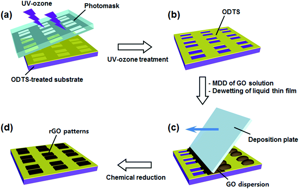 | ||
| Fig. 1 Schematic illustration of the surface energy guided patterning process. (a) ODTS-treated substrate (covered with photomask) was treated with UV-ozone. (b) After UV-ozone treatment, ODTS patterns were formed. (c) Dragging the GO solution on the ODTS patterned substrate by applying the meniscus dragging deposition (MDD) method. (d) Chemical reduction of the GO patterns with 2:5 HI:acetic acid vapor at 80 °C. | ||
A set of straight line patterns with different spacings and widths was fabricated to confirm that the dewetting propagated completely at various spacing lengths and pattern widths. Fig. 2a shows an array of 40 μm wide and 25 mm-long line patterns with varying spacings from 50 μm to 800 μm and Fig. 2b shows a straight-line pattern with 10 μm, 20 μm, and 40 μm widths taken using an optical microscope. These patterns were fabricated under conditions of 15° deposition plate angle, 2.94 mm s−1 deposition velocity, and 3 μL GO solution with 6.65 mg mL−1 GO concentration. As shown in Fig. 2a and b, the patterns were clearly defined over the tested range of spacings and widths. To study the morphological features, FE-SEM and AFM images were taken, as in Fig. 2c and d. As shown in the FE-SEM image, rGO was deposited only on the desired area, forming a clear pattern edge. It was because the GO solution was completely dewetted from the ODTS layer. It was confirmed from the AFM image that a large number of rGO flakes were uniformly deposited without the coffee-ring effect that is usually observed when aqueous GO solution is used directly for patterning.27 Suppression of the coffee-ring effect resulted from the high viscosity of concentrated GO solution. The coffee-ring effect is caused by the evaporation-induced radial migration of particles. However, as viscosity is increased, radial migration is suppressed by the viscous force.27 In this study, highly concentrated GO solution (6.65 mg mL−1) was used and the dynamic viscosity of the solution was measured as 234 mPa s, which is hundreds of times larger than that of low-concentrated GO solution. Therefore, the GO flakes inside the liquid film were barely mobile and able to stack uniformly without the coffee-ring effect.
 | ||
| Fig. 2 (a) Optical microscopy images of rGO line patterns (40 μm wide and 25 mm long with various line-spacings from 50 to 800 μm). (b) Optical microscopy images of rGO line patterns with a width of 10, 20, and 40 μm. (c) FE-SEM image of 40 μm wide rGO line patterns. (d) Topography and thickness of rGO line patterns measured by AFM. The rGO line patterns were prepared by the MDD with a deposition angle of 15°, a deposition speed of 2.94 mm s−1, and a GO concentration of 6.65 mg mL−1. | ||
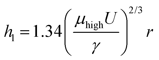
The influences of coating conditions including GO concentration, deposition velocity, and deposition angle were studied. The 20 μm wide patterns were fabricated based on the conditions of 15° deposition angle, 2.94 mm s−1 deposition speed, and 6.65 mg mL−1 GO concentration, unless otherwise noted. Fig. 3 shows a plot of rGO pattern thickness and actual rGO pattern width with respect to each variable condition. The delicate control of rGO thickness was carried out by adjusting the GO concentration, as shown in Fig. 3a. The thickness of the film increased linearly from 2.5 nm to 13.5 nm while the concentration increased from 2 mg mL−1 to 6.65 mg mL−1. This can be simply explained by higher GO content in the more concentrated solution. The influences of deposition velocity and deposition angle on rGO thickness are plotted in Fig. 3b and c. In both cases, the thickness of the pattern increased as the deposition angle or speed increased. For further characterization, the I–V characteristic curve of rGO patterns prepared with different deposition speeds is shown in Fig. S3 (ESI†). As the deposition speed was increased, the rGO line pattern exhibits higher electrical conductivity because the produced pattern became thicker. This dependence of pattern thickness can be explained by the Landau–Levich–Derjaguin (LLD) model,29,35
 | (1) |
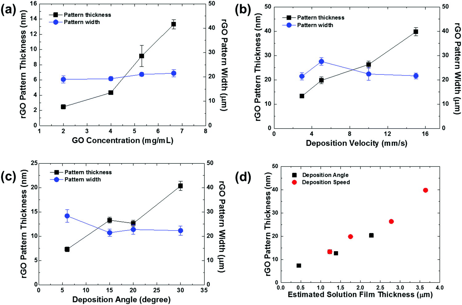 | ||
| Fig. 3 Thickness and width of rGO line patterns as a function of (a) GO concentration (deposition angle = 15°, deposition velocity = 2.94 mm s−1), (b) deposition velocity (GO concentration = 6.65 mg mL−1, deposition angle = 15°), and (c) deposition angle (GO concentration = 6.65 mg mL−1, deposition velocity = 2.94 mm s−1). The rGO patterns were formed on ODTS pre-patterned substrates with a quartz chrome mask containing 20 μm-wide line pattern design. (d) rGO pattern thickness as a function of estimated liquid film thickness based on eqn (1) by varying the deposition angle and deposition speed. | ||
For further characterization, dewetting kinetics was also studied. The relative time scale of dewetting and drying, tdewet/tdry, is an important parameter for determining whether a well-defined pattern is obtainable. A well-defined pattern can only be implanted when the liquid film is completely dewetted from the hydrophobic surface before drying. At the same time, the liquid film on the hydrophilic surface should not be dewetted until it is dried completely. The coating conditions are determined by estimating the value of the relative time scale, tdewet/tdry. The time for dewetting was calculated from L/Vdewet, where Vdewet is the dewetting velocity defined as the shrinking velocity of the edge line of the liquid film and L is the characteristic length of dewetting. In this study, the maximum spacing between patterns was 800 μm. The dewetting velocity was calculated from the hydrodynamic properties of the solution,43
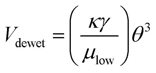 | (2) |
The rGO line patterns prepared at slower deposition velocity and smaller deposition angle showed relatively large deviation of the pattern width (Fig. 3b and c), because the GO flakes are deposited on the substrate before complete dewetting of the thinner liquid films due to fast drying time. However, the rGO micropatterns formed in the thicker liquid films at higher deposition speeds and angles exhibit the pre-programmed pattern width due to complete dewetting of the liquid films on the hydrophobic region before film drying.
Patterns of various shapes were successfully fabricated through the surface energy guided patterning technique. These patterns were coated at 15° deposition angle, 2.94 mm s−1 deposition speed, and 6.65 mg mL−1. Optical images of circles, meshes, triangles, concentric circles, squares, and an alphabet are illustrated in Fig. 4. As shown, delicate control of dewetting the liquid films can be carried out by our surface energy guided patterning technique. An organic field effect transistor (OFET) was fabricated to verify the applicability of our rGO patterning method, as shown in Fig. 5. On a selectively pre-patterned rGO electrode, DPP–DTT was coated by the MDD method. Fig. 5b illustrates the structure of the device. The rGO pattern was used for source–drain electrodes. Fig. 5c shows our well-defined full solution processed OFET.
 | ||
| Fig. 4 Various patterned rGO microstructures on ODTS pre-treated glass substrates. Optical microscopy images of (a) circle arrays, (b) triangle arrays, (c) square arrays, (d) grids, (e) concentric circles, and (f) alphabet ‘u’. The rGO patterns were prepared by the MDD with a deposition angle of 15°, a deposition speed of 2.94 mm s−1, and a GO concentration of 6.65 mg mL−1. | ||
 | ||
| Fig. 5 (a) Schematic of the deposition of the DPP–DTT thin film on rGO patterned Si/SiO2 by the MDD coating method. (b) Schematic diagram of the OFET with rGO source–drain electrodes. (c) Optical micrograph of OFET arrays with rGO electrodes on Si/SiO2. | ||
Near edge X-ray absorption fine structure spectroscopy (NEXAFS) measurements were performed to conduct a comparative study of the crystallite-orientations of DPP–DTT molecules deposited on ODTS (channel area), Au (electrode area), and rGO (electrode area). We obtained the average tilting angle of the polymer backbone against the substrate by analyzing NEXAFS spectra measured from various incident X-ray angles. The NEXAFS spectra of DPP–DTT deposited on ODTS, Au, and rGO are summarized in Fig. 6(a), (b), and (c), respectively. By plotting the π* resonance (284–286 eV) as a function of cos 2θ, where θ is the incident angle, we obtained the dichroic ratio (R) and the average tilting angle (α) of the polymer backbone.45 As summarized in Fig. 6(d–f), the azimuthal average tilting angles α of DPP–DTT were ∼77.5° (R = 0.62), ∼75° (R = 0.56), and ∼75.4° (R = 0.58) for depositions on ODTS, Au, and rGO, respectively. These results (α > 70°) implied that in all cases, DPP–DTT preferentially adopted an edge-on orientation rather than a face-on orientation against the substrate. The highest tilting angle of DPP–DTT on ODTS reflected the highest hydrophobicity of the densely packed self-assembled ODTS monolayer. In a similar context, the lowest tilting angle on Au was attributed to the highest surface energy of the Au metal surface. In other words, DPP–DTT molecules deposited on rGO and those deposited on ODTS were continuously connected to each other, unlike the cases of Au and ODTS. Therefore, the DPP–DTT molecules deposited on a rGO(electrode)/ODTS(channel) device had smaller orientational differences at the electrode/channel interface than the Au/ODTS device.
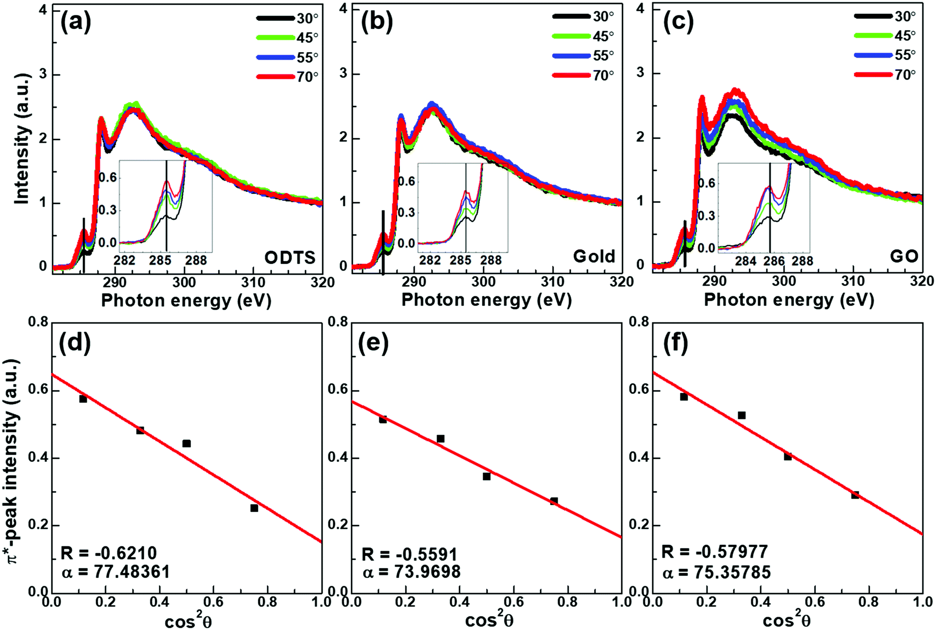 | ||
| Fig. 6 (a–c) NEXAFS spectra of DPP–DTT films deposited on (a) ODTS, (b) Au, and (c) rGO. (d–f) Their corresponding π* resonance intensity versus incident angle relationships. | ||
In OFETs, very often differences in crystallite orientation present at the electrode/channel interfaces directly induce increases in contact resistance. The effective electric field applied to the semiconductor channel is greatly reduced by this unprecedented emergence of contact resistance. The resultant OFET showed lower performance than the ideal Ohmic contact. Therefore, in the OFETs with precisely patterned rGO developed in this study, one could expect lower contact resistance than conventional Au-based OFETs, as discussed in the NEXAFS section. To prove our hypothesis, the transfer-length method (TLM) was used to measure contact resistances of OFETs with Au and rGO source–drain electrodes.46 In this method, the total source–drain resistance (Rtot) was obtained from the relation  .47 Here VD is the measured drain voltage and ID the measured drain current present in the linear regime of the output curve (VDvs. ID characteristics). The channel width (W)-normalized Rtot value was then plotted as a function of channel length (L), as summarized in Fig. 7(a and b). From extrapolation to L = 0, we obtained the contact resistance, Rc.48 As shown in Fig. 7(c), for various gate voltages applied, the Rc values of rGO-based OFETs were apparently lower than those of Au-based OFETs by more than four times. Collectively, NEXAFS and contact resistance studies showed that the rGO electrode can be a better choice for source–drain electrodes in OFETs rather than conventional Au due to the former's better role as electrodes such as lower contact resistance, enabled by the near-continuous crystalline orientation with top-deposited organic semiconductors.
 | ||
| Fig. 7 (a) Channel-width-normalized resistance of an Au-electrode device as a function of channel length at various gate voltages at a drain voltage of −100 V. (b) Channel-width-normalized resistance of a rGO-electrode device as a function of channel length at various gate voltages at a drain voltage of −100 V. (c) Channel-width-normalized contact resistances of Au and rGO-electrode devices as a function of gate voltage. | ||
As the last step, we optimized bottom-contact/bottom-gate OFETs using both Au and rGO electrodes. The resultant transfer and output characteristics are summarized in Fig. 8. Reflecting remarkable decreases in contact-resistance as a result of decreased orientational differences at the electrode/channel interface, the rGO-based OFETs rendered greatly enhanced transistor performances relative to Au-based OFETs. The field effect mobility as high as 0.6 cm2 (V s)−1 was obtained from the rGO-based OFETs while a two times lower mobility of 0.3 cm2 (V s)−1 was obtained from Au-based OFETs. The on/off ratio was also significantly higher in the case of rGO-based OFETs (1.79 × 10⁶) relative to the Au-based ones (8.63 × 10⁴). This was due to the low conductivity of rGO-based OFETs at zero gate bias without the introduction of charge carriers by the field-effect, achieved by defect-free electrode/channel interfaces.
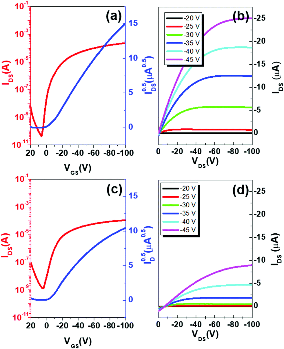 | ||
| Fig. 8 Transfer (left) and output (right) characteristics of OFETs. The transfer curves were measured in a saturation regime with VDS = −100 V. The upper (a and b) and lower (c and d) panels correspond to rGO-based OFETs (W/L = 22) and Au-based OFETs (W/L = 20), respectively. | ||
Conclusions
We succeeded in fabricating high-resolution rGO patterns including circles, triangles, squares, meshes, and concentric circles, which are rarely achieved using aqueous GO dispersions. This patterning was driven by inducing partial dewetting of liquid films due to high surface energy differences between the pre-patterned hydrophilic and hydrophobic layers. The thickness of the patterns was easily tuned by controlling coating parameters such as deposition speed, deposition angle, and GO concentration. Suppression of the coffee-ring effect, which was a major obstacle to using GO dispersions directly in patterning, was successfully conducted using a highly concentrated GO dispersion. The high performance of OFETs with the patterned rGO electrodes also demonstrated that our patterning method can be used in the field of optoelectronics. This surface energy guided patterning technique did not require rigid conditions such as high vacuum and/or high temperature. The rGO patterns could be implemented in a short period of time. Thus, our simple and scalable patterning method of the rGO electrodes would contribute to research into next-generation optoelectronic devices.Conflicts of interest
There are no conflicts to declare.Acknowledgements
This work was supported by the National Research Foundation of Korea (NRF) grant funded by the Korea government (MSIP) (No. 2016R1A2B4012992) and the Chung-Ang University Graduate Research Scholarship in 2017.References
- A. K. Geim and K. S. Novoselov, Nat. Mater., 2007, 6, 183–191 CrossRef CAS.
- D. Akinwande, N. Petrone and J. Hone, Nat. Commun., 2014, 5, 5678 CrossRef CAS PubMed.
- P. C. Ooi, M. A. S. M. Haniff, M. F. M. R. Wee, C. F. Dee, B. T. Goh, M. A. Mohamed and B. Y. Majlis, Carbon, 2017, 124, 547–554 CrossRef CAS.
- D. Konios, C. Petridis, G. Kakavelakis, M. Sygletou, K. Savva, E. Stratakis and E. Kymakis, Adv. Funct. Mater., 2015, 25, 2213–2221 CrossRef CAS.
- D. S. Chung, S. M. Lee, J. Y. Back, S. K. Kwon, Y. H. Kim and S. T. Chang, ACS Appl. Mater. Interfaces, 2014, 6, 9524–9529 CrossRef CAS PubMed.
- W. K. C. Yung, G. Li, H. M. Liem, H. S. Choy and Z. Cai, J. Mater. Chem. C, 2015, 3, 11294–11299 RSC.
- D. Zaharie-Butucel, L. Digianantonio, C. Leordean, L. Ressier, S. Astilean and C. Farcau, Carbon, 2017, 113, 361–370 CrossRef CAS.
- Y. J. Yun, J. Ju, J. H. Lee, S. H. Moon, S. J. Park, Y. H. Kim, W. G. Hong, D. H. Ha, H. Jang, G. H. Lee, H. M. Chung, J. Choi, S. W. Nam, S. H. Lee and Y. Jun, Adv. Funct. Mater., 2017, 27, 1701513 CrossRef.
- B. Saha, S. Baek and J. Lee, ACS Appl. Mater. Interfaces, 2017, 9, 4658–4666 CrossRef CAS PubMed.
- B. Yin, Y. Wen, T. Hong, Z. Xie, G. Yuan, Q. Ji and H. Jia, ACS Appl. Mater. Interfaces, 2017, 9, 32054–32064 CrossRef CAS.
- T. Y. Choi, B. U. Hwang, B. Y. Kim, T. Q. Trung, Y. H. Nam, D. N. Kim, K. Eom and N. E. Lee, ACS Appl. Mater. Interfaces, 2017, 9, 18022–18030 CrossRef CAS PubMed.
- J. Kim, M. S. Chae, S. M. Lee, D. Jeong, B. C. Lee, J. H. Lee, Y. Kim, S. T. Chang and K. S. Hwang, Sci. Rep., 2016, 6, 31276 CrossRef CAS PubMed.
- W. Yuan and G. Shi, J. Mater. Chem. A, 2013, 1, 10078–10091 RSC.
- C. Chung, Y. K. Kim, D. Shin, S. R. Ryoo, B. H. Hong and D. H. Min, Acc. Chem. Res., 2013, 46, 2211–2224 CrossRef CAS PubMed.
- C. Ogata, R. Kurogi, K. Awaya, K. Hatakeyama, T. Taniguchi, M. Koinuma and Y. Matsumoto, ACS Appl. Mater. Interfaces, 2017, 9, 26151–26160 CrossRef CAS PubMed.
- C. Shao, T. Xu, J. Gao, Y. Liang, Y. Zhao and L. Qu, Nanoscale, 2017, 9, 12324–12329 RSC.
- X. Yun, Z. Xiong, L. Tu, L. Bai and X. Wang, Carbon, 2017, 125, 308–317 CrossRef CAS.
- C. Soldano, A. Mahmood and E. Dujardin, Carbon, 2010, 48, 2127–2150 CrossRef CAS.
- W. Ren and H. M. Cheng, Nat. Nanotechnol., 2014, 9, 726–730 CrossRef CAS.
- R. Muñoz and C. Gómez-Aleixandre, Chem. Vap. Deposition, 2013, 19, 297–322 CrossRef.
- K. R. Paton, E. Varrla, C. Backes, R. J. Smith, U. Khan, A. O’Neill, C. Boland, M. Lotya, O. M. Istrate, P. King, T. Higgins, S. Barwich, P. May, P. Puczkarski, I. Ahmed, M. Moebius, H. Pettersson, E. Long, J. Coelho, S. E. O’Brien, E. K. McGuire, B. M. Sanchez, G. S. Duesberg, N. McEvoy, T. J. Pennycook, C. Downing, A. Crossley, V. Nicolosi and J. N. Coleman, Nat. Mater., 2014, 13, 624–630 CrossRef CAS PubMed.
- D. R. Dreyer, S. Park, C. W. Bielawski and R. S. Ruoff, Chem. Soc. Rev., 2010, 39, 228–240 RSC.
- S. Pei and H. M. Cheng, Carbon, 2012, 50, 3210–3228 CrossRef CAS.
- G. Eda and M. Chhowalla, Adv. Mater., 2010, 22, 2392–2415 CrossRef CAS.
- J. Li, F. Ye, S. Vaziri, M. Muhammed, M. C. Lemme and M. Östling, Adv. Mater., 2013, 25, 3985–3992 CrossRef CAS PubMed.
- F. Torrisi, T. Hasan, W. Wu, Z. Sun, A. Lombardo, T. S. Kulmala, G. W. Hsieh, S. Jung, F. Bonaccorso, P. J. Paul, D. Chu and A. C. Ferrari, ACS Nano, 2012, 6, 2992–3006 CrossRef CAS.
- P. He and B. Derby, Adv. Mater. Interfaces, 2017, 4, 1700944 CrossRef.
- M. W. Jung, S. Myung, W. Song, M. A. Kang, S. H. Kim, C. S. Yang, S. S. Lee, J. Lim, C. Y. Park, J. O. Lee and K. S. An, ACS Appl. Mater. Interfaces, 2014, 6, 13319–13323 CrossRef CAS.
- N. H. Kim, B. J. Kim, Y. Ko, J. H. Cho and S. T. Chang, Adv. Mater., 2013, 25, 894–898 CrossRef CAS.
- M. W. Jung, S. Myung, K. W. Kim, W. Song, Y. Y. Jo, S. S. Lee, J. Lim, C. Y. Park and K. S. An, Nanotechnology, 2014, 25, 285302 CrossRef.
- J. Zhang, P. Hu, R. Zhang, X. Wang, B. Yang, W. Cao, Y. Li, X. He, Z. Wang and W. O’Neill, J. Mater. Chem., 2012, 22, 714–718 RSC.
- Y. Tu, H. Nakamoto, T. Ichii, T. Utsunomiya, O. P. Khatri and H. Sugimura, Carbon, 2017, 119, 82–90 CrossRef CAS.
- Y. Xue, L. Zhu, H. Chen, J. Qu and L. Dai, Carbon, 2015, 92, 305–310 CrossRef CAS.
- Y. Tu, T. Ichii, T. Utsunomiya and H. Sugimura, Appl. Phys. Lett., 2015, 106, 133105 CrossRef.
- Y. U. Ko, S. Cho, K. S. Choi, Y. Park, S. T. Kim, N. H. Kim, S. Y. Kim and S. T. Chang, J. Mater. Chem., 2012, 22, 3606–3613 RSC.
- J. Z. Wang, Z. H. Zheng, H. W. Li, W. T. S. Huck and H. Sirringhaus, Nat. Mater., 2004, 3, 171–176 CrossRef CAS.
- B. R. Yang, W. Cao, G. S. Liu, H. J. Chen, Y. Y. Noh, T. Minari, H. C. Hsiao, C. Y. Lee, H. P. D. Shieh and C. Liu, ACS Appl. Mater. Interfaces, 2015, 7, 21433–21441 CrossRef CAS.
- S. Fujii, T. Tanaka, H. Suga, Y. Naitoh, T. Minari, K. Tsukagoshi and H. Kataura, Phys. Status Solidi B, 2010, 247, 2750–2753 CrossRef CAS.
- M. H. Jung and H. S. Choi, Korean J. Chem. Eng., 2009, 26, 1778–1784 CrossRef CAS.
- B. Arkles, Hydrophobicity, Hydrophilicity and Silane Surface Modification, Gelest, 2011 Search PubMed.
- D. W. Moon, A. Kurokawa, S. Ichimura, H. W. Lee and I. C. Jeon, J. Vac. Sci. Technol., A, 1999, 17, 150–154 CrossRef CAS.
- J. R. Vig, J. Vac. Sci. Technol., A, 1985, 3, 1027–1034 CrossRef CAS.
- C. Redon, F. Brochard-Wyart and F. Rondelez, Phys. Rev. Lett., 1991, 66, 715–718 CrossRef CAS PubMed.
- B. Dan, G. C. Irvin and M. Pasquali, ACS Nano, 2009, 3, 835–843 CrossRef CAS.
- D. S. Chung, J. W. Park, S. Kim, K. Heo, C. E. Park, M. Ree, Y. Kim and S. Kwon, Chem. Mater., 2009, 21, 5499–5507 CrossRef CAS.
- C. Liu, Y. Xu and Y.-Y. Noh, Mater. Today, 2015, 18, 79–96 CrossRef CAS.
- B. H. Hamadani and D. Natelson, Appl. Phys. Lett., 2004, 84, 443–445 CrossRef CAS.
- P. V. Necliudov, M. S. Shur, D. J. Gundlach and T. N. Jackson, Solid-State Electron., 2003, 47, 259–262 CrossRef CAS.
Footnotes |
| † Electronic supplementary information (ESI) available: Contact angle measurement of an ODTS treated substrate and an UV/O3 treated substrate, and calculation of the relative time scale between dewetting and drying of liquid thin films. See DOI: 10.1039/c8tc03981j |
| ‡ These authors contributed equally to this work. |
| This journal is © The Royal Society of Chemistry 2019 |