
 Open Access Article
 This Open Access Article is licensed under a
 Creative Commons Attribution 3.0 Unported Licence
UV–O3 treated annealing-free cerium oxide as electron transport layers in flexible planar perovskite solar cells†
Aiying
Pang
ab,
Jinlong
Li
ac,
Xiao-Feng
Wei
d,
Zhi-Wu
Ruan
ab,
Ming
Yang
ab and
Zhong-Ning
Chen
 *ab
*ab
aState Key Laboratory of Structural Chemistry, Fujian Institute of Research on the Structure of Matter, Chinese Academy of Sciences, Fuzhou, Fujian 350002, China
bCollege of Chemistry and Materials, Fujian Normal University, Fuzhou, Fujian 350007, China
cCollege of Chemistry, Fuzhou University, Fuzhou, Fujian 350002, China
dNational Engineering Research Center of Chemical Fertilizer Catalyst, School of Chemical Engineering, Fuzhou University, Fujian 350002, China
First published on 23rd July 2020
Abstract
Fabricating electron transport layers at low temperatures is challenging but highly desired in the field of flexible perovskite solar cells (f-PSCs). In this study, highly uniform cerium oxide (CeOx) films prepared by the UV–O3 treatment have been successfully applied as the electron transport layer (ETL) in methylammonium lead halide (CH3NH3PbI3) perovskite-based f-PSCs. Under AM 1.5 G sunlight with 100 mW cm−2, these cells exhibited an open-circuit voltage (Voc) of 0.98 V, a short-circuit current density (Jsc) of 19.42 mA cm−2, a fill factor (FF) of 0.72 and power conversion efficiency (PCE) of 14.63%. The PCE was much higher than that of the control planar CeOx ETL (PCE ∼ 9.08%) prepared at a low temperature (80 °C) without the UV–O3 treatment, and this was ascribed to the improved CeOx film, enhanced light absorption and suppressed charge recombination. The cells that bend at 15 mm of radius showed excellent stability with less than 10% reduction in PCE after 500 cycles of repeated bending at ambient temperature. The charge-transmission kinetic parameters and long-term stability of the CeOx-based f-PSCs were analyzed as well.
1. Introduction
Perovskite solar cells (PSCs) are very promising devices in photovoltaic applications due to their impressive efficiency increasing and efficient energy harvesting. Most academic and industrial researches have been focused on PSCs immobilized on rigid substrates.1,2 However, rigid glass substrates are generally fragile and difficult for scale-up utilization. Incontrovertibly, the flexible perovskite solar cells (f-PSCs) hinged on plastic substrates, which are readily bendable and expediently portable, are suitable for wearable electricity-generating devices and building integrated photovoltaics. In fact, relevant advancements in n–i–p planar or p–i–n cells on plastic substrates achieved the highest reported power conversion efficiency (PCE) of 20.01%.3–5 Apart from the high PCE, this new photovoltaic technology can be achieved using low temperatures (<150 °C) to convert the perovskite and electron transport layer (ETL) precursors into their final semiconducting forms, which are then immobilized onto transparent plastic substrates, such as polyethylene naphthalate (PEN) and polyethylene terephthalate (PET).Nevertheless, some new obstacles have been found in f-PSCs. Titanium oxide (TiO2), the most widely used material in the compact layer and mesoporous layer (collectively called ETL) in the regular architecture of PSCs, typically sustains high-temperature treatment (500 °C).6,7 This is incompatible with plastic substrates, whose processing temperature must be controlled below 150 °C. Till now, only one study has reported the use of mesoporous TiO2 in f-PSCs made of polymer films,8 whereas it is more regularly used on metal-foil substrates that can endure high temperatures.9 In addition, Nb-doped TiO2 ETLs fabricated via a low-temperature (<50 °C) UV process exhibited the best PCE of 16.01% when used in n–i–p f-PSCs.10 ETLs generated from Ti-based metal–organic framework nanoparticles at ambient temperature have been found suitable for charge injection and transfer from the perovskite to the electrodes.11 Although a TiOx-based ETL prepared through a low-temperature (<100 °C) solution process has achieved up to 17.6% of PCE, TiO2-based PSCs can be easily destroyed by UV light.12 This intrinsic property inhibits the commercial applications of TiO2-based PSCs.13,14 ZnO is considered as the most promising material for f-PSCs because it has the same conduction band at 3.2 eV as that of TiO2, a higher electron mobility of 115–155 cm2 V−1 s−1 and especially an easier low-temperature synthetic process.15,16 When a mesoporous layer grown from ZnO nanorods using a chemical bath was first implemented in f-PSCs, it showed a PCE of 5.0% on PET/ITO, showing a great prospect.16 The ink-dispersed ZnO nanoparticles fabricated by the spin-coating process are widely employed as ETLs in inverted devices.17,18 The planar solar cell configuration of PEN/ITO/ZnO/CH3NH3PbI3/PTAA/Au delivered the highest efficiency of 15.6% at the time of publication.19 However, the hydroxide groups in the ZnO nanoparticles are very susceptible to acid and base solutions, which is detrimental to the long-term stability of f-PSCs, leading to the degradation of the perovskite layer.20,21 Alternatively, SnO2 is a UV- and chemical-stable material for PSCs with a larger bandgap and higher electron mobility than TiO2 and ZnO.22,23 The f-PSCs based on solution-processing SnO2 ETLs could achieve a PCE of 17.21%; however, the processing temperature of up to 180 °C is far greater than the maximum tolerable temperature (150 °C) of the flexible substrates.24 On the other hand, though SnOx prepared by atomic layer deposition satisfies the temperature requirements and exhibits good electron selectivity, the fabrication process inhibits its application in roll-to-roll technology and commercial appeal.25,26 Therefore, it is necessary to search for new type ETLs with processing temperatures under 150 °C and enhance long-term stability.
Cerium oxide (CeOx) has a wide bandgap with an effective dielectric constant, good transparency, sufficient ionic conductivity, and high-temperature stability, and has been used in various optoelectronic applications, such as light absorber in organic-dye-free solar cells, photoanode in-dye sensitized solar cells, and antireflection coating in silicon solar cells.27,28 It is worth noting that CeOx used recently in PSCs exhibited better photoelectric properties under 6,6-phenyl-C61-butyric acid methyl ester modification or when employed as a dense diffusion barrier in the p–i–n structure.29,30 In this study, we report CeOx aqueous sol–gel as a precursor for ETL preparation by the UV–O3 treatment for use in flexible n–i–p planar PSCs in the quest for a low-cost and scale-up manufacturing technology. The compact CeOx layers treated by low-temperature annealing (LT-CeOx), ultraviolet–ozone (UV–O3) (UV-CeOx), and a co-processing treatment (UV/LT-CeOx) were characterized by studying the hydrophilicity contact angle and surface behavior. In order to verify the difference of device ETLs, photoelectric tests of the cells with, as well as without UV–O3 treatment, were carried out. As demonstrated experimentally, the UV–O3-treatment of the compact CeOx layer imparted a positive effect on the cell performance, improving the efficiency from 9.08% to over 14%.
2. Experimental section
2.1 CeOx sol–gel solution preparation
CeOx NCs were synthesized by a modified procedure described in the literature.31 6.0 g of Ce(NO3)3·6H2O (99%, Aldrich) was added to 70 mL distilled water with stirring till it was sufficiently dissolved. An NH4OH (NH3 content 28–30%, Aldrich, ACS reagent) solution was then added dropwise until a pH of 10 was reached. Then, cerium nitrate completely converted to cerium hydroxide and precipitated, which was separated by centrifugation and washed with deionized water repeatedly. Then, it was dissolved in 140 mL of a 0.1 M urea aqueous solution and adjusted to pH 2 by the addition of dilute hydrochloric acid (10%). The concentration of the obtained solution was assessed as 82 mM by calculating its xerogels at 600 °C for 2 h. The obtained CeOx sol–gel solution was stored at room temperature to prepare ETLs.2.2 CH3NH3I preparation
CH3NH3I was synthesized and purified using a method described in the literature.32 10 mL hydroiodic acid (57 wt%) was added dropwise with stirring to a 33 wt% methanol solution of methylamine (24 mL) at the temperature of 0 °C. After stirring for 2 h in an N2 atmosphere, the obtained liquid–solid mixture was evaporated by a liquid-volatile separation process at 50 °C for 1 h to remove volatile substances. Then, the resultant crystal was permeated with three 70 mL portions of absolute diethyl ether and dried at 60 °C in a vacuum oven for 12 h to afford the desired product with high purity.2.3 Device fabrication
ITO-coated flexible substrates (polyethylene naphthalate, PEN) were sequentially cleaned by acetone and ethanol for 15 min and then by UV–ozone (UV–O3) treatment for another 15 min. The cleaned flexible substrates were spin-coated with the CeOx colloid for 30 s at 2000 rpm. The UV-CeOx ETLs were obtained after drying at 80 °C for 10 min and exposure to UV–O3 for 15 min. The LT-CeOx ETLs were obtained just by drying at 80 °C for 20 min. Identical processes and treating conditions were repeated for adjusting the thickness of the ETLs. After that, the ETLs were infiltrated with the perovskite precursor solution by the spin-coating process in a glovebox under a nitrogen atmosphere. The perovskite precursor solution was prepared using a stoichiometric amount of CH3NH3PbI3 in 1.2 M DMSO with lead iodide and methyl ammonium iodide at a molar ratio of 1![[thin space (1/6-em)]](https://www.rsc.org/images/entities/char_2009.gif) :1.32 The spin coating procedure was firstly performed at 6000 rpm for 20 s and then for 10 s by gently dropping chlorobenzene on the spinning substrate with a micropipette. Then, the substrate was heated at 100 °C for 1 h on a hot plate in the glovebox. After they were cooled to 25 °C, the spiro-OMeTAD solution (60 μL) was spin-coated on the CH3NH3PbI3 layer at 3000 rpm for 20 s to be used as the hole transparent layer. Spiro-OMeTAD was dissolved in chlorobenzene at 72 mg mL−1, to which 28.8 μL of 4-tert-butyl pyridine and 14.4 μL of lithium bis(trifluoromethanesulfonyl)-imide (Li-TFSI) solution (520 mg Li-TFSI in 1 mL acetonitrile) were added. Finally, an 80 nm gold layer was deposited on the coated spiro-OMeTAD film at ∼10−6 bar via thermal evaporation.
:1.32 The spin coating procedure was firstly performed at 6000 rpm for 20 s and then for 10 s by gently dropping chlorobenzene on the spinning substrate with a micropipette. Then, the substrate was heated at 100 °C for 1 h on a hot plate in the glovebox. After they were cooled to 25 °C, the spiro-OMeTAD solution (60 μL) was spin-coated on the CH3NH3PbI3 layer at 3000 rpm for 20 s to be used as the hole transparent layer. Spiro-OMeTAD was dissolved in chlorobenzene at 72 mg mL−1, to which 28.8 μL of 4-tert-butyl pyridine and 14.4 μL of lithium bis(trifluoromethanesulfonyl)-imide (Li-TFSI) solution (520 mg Li-TFSI in 1 mL acetonitrile) were added. Finally, an 80 nm gold layer was deposited on the coated spiro-OMeTAD film at ∼10−6 bar via thermal evaporation.
2.4 Characterization
The XRD patterns were measured on a PANalytical X'Pert spectrometer using Co Kα radiation (λ = 1.78897 Å), and the data were converted to Cu Kα data. SEM was performed on a Hitachi S4800 instrument. TEM and SAED pattern images were recorded on a Tecnai G2 F20 (FEI) with an accelerated photo-voltage of 200 kV. The FT-IR spectra were obtained on a PerkinElmer Spectrum 2000. The survey scans were recorded using monochromatic Al Kα irradiation, 1 eV steps and an 80 eV analyser. The transmittance spectra and UV-vis spectra were measured on a Lambda-9 (PerkinElmer) spectrometer. The steady-state photoluminescence (PL) and time-resolved photoluminescence (TRPL) decay spectra of CH3NH3PbI3 coated on the LT-CeOx, LT-CeOx, and UV/LT-CeOx ETLs were recorded using an Edinburgh FLS920 instrument with a picosecond-pulsed diode laser at 375 nm. The UPS for the LT-CeOx, LT-CeOx, and UV/LT-CeOx ETLs were measured using ESCALAB 250Xi (Thermo Fisher) under a background pressure of 5.0 × 10⁻⁷ Pa.The photovoltaic performance in terms of J–V characteristics was measured on a solar simulator (Sol3A Class AAA, Oriel Instruments, Stratford, CT, USA) and a Keithley 2440 source measurement unit (Keithley Instruments Inc., Cleveland, OH, USA) under 1.5 air mass (AM) and 1 sun (100 mW cm−2) condition. The 1-sunlight intensity level was calibrated using a standard Si reference cell certified by the Newport Corporation. All the devices were measured in a light-tight sample holder with an active area of 0.12 cm2 for each cell and fixed using an aperture mask. IPCE was measured using a quantum efficiency measurement system (QEX10, PV Measurements, Inc.) in the wavelength range of 300 to 850 nm. EIS was recorded using a potentiostat (IM-6, Zahner) in the frequency range of 0.1 to 100 kHz by applying the Voc values derived from the J–V tests and under dark conditions.
3. Results and discussion
The ligand-capped CeOx sol–gel solution prepared using a 0.1 M aqueous urea solution displayed dense uniform dispersion in deionized water without conglomeration (Fig. 1a), which is necessary for making stable, void-free and gap-filling CeOx thin films on flexible PEN substrates. However, the cross-linking of the organic ligands in the CeOx sol–gel solution may hinder the charge transport and deteriorate the photovoltaic performance. With this in mind, we utilized a convenient UV–O3-processing approach to help the decomposition of organic ligands at a low temperature and reduce the spontaneous coalescence of the CeOx nanocrystals (NCs) during preparation, thus producing high-quality ETLs. As presented in Fig. 1a, the urea-chelated CeOx NCs self-organized into free-standing thin films by capillary-force-induced clustering of the dispersing medium during preparation.33 Under ozone and UV-light irradiation (UV–O3), oxygen-free radicals decomposed the urea ligands bound to the CeOx NCs into NH3, CO2, and H2O. As the organic ligands decomposed, the CeOx NCs would congregate on plastic substrate, finally leading to the direct attachment of the CeOx film. Without the UV–O3 treatment, pinhole-free CeOx thin films were successfully fabricated by the low-temperature reaction at 80 °C. In this paper, we made the first endeavor to create a dense CeOx layer via ancillary ligand decomposition by applying UV–O3 without heat treatment. The crystal structures of the CeOx NCs before and after the UV–O3 treatment were demonstrated by the X-ray diffraction (XRD) patterns. As shown in Fig. 1b, all the peaks in the XRD patterns of LT-CeOx and UV-CeOx were assignable to the cubic fluorite crystal structure (PDF no. 34-0394). We found that there was no significant difference in the microstructure between the CeOx films obtained with and without UV–O3 treatment. As depicted in Fig. 1c, the decomposition of the organic ligands was demonstrated by the Fourier-transform infrared (FT-IR) spectra of the CeOx films obtained with and without UV–O3 treatment. The bands around 3400 cm−1 and 1630 cm−1 could be ascribed to O–H stretching and bending vibrations, respectively, which are indicative of the remaining water molecules and the surface hydroxyl groups of the CeOx thin films. The peak near 1127 cm−1 might be from the C–N stretching vibration of urea,34 while the peak at 1382 cm−1 was due to the deformation of ammonium produced by urea decomposition.35 Since both these peaks disappeared entirely after UV–O3 exposure for more than 30 min, urea was entirely decomposed by free radicals under UV irradiation. The band at 1496 cm−1 was ascribed to the stretching vibration of the carboxylates formed from urea decomposition.36 Lastly, the band near 480 cm−1 in the finger-print region corresponded to the vibrational stretching of the Ce–O bond formed under UV–O3 treatment. Furthermore, the removal of hydrophobic molecules achieved by this simple yet efficient method was confirmed by the improved wettability of the CeOx film in hybrid perovskite solar cells because of the hydrophilic surface of CeOx (Fig. S1 and S2†).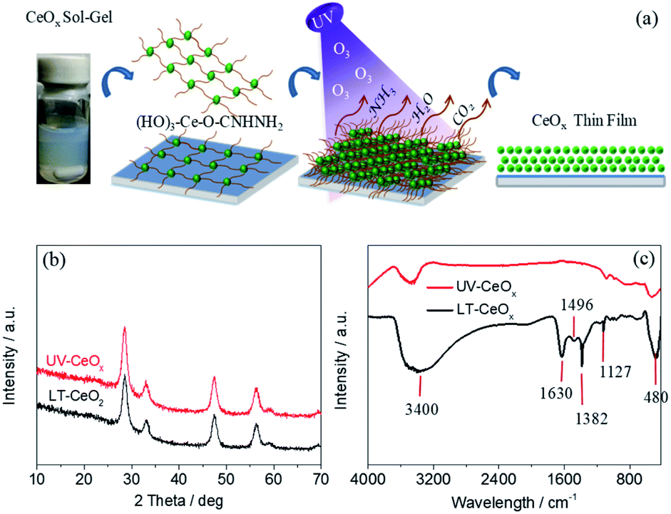 | ||
| Fig. 1 (a) Schematic illustration of the UV–O3 process for the preparation of CeOx thin films. (b) XRD spectra and (c) FT-IR spectra of the CeOx thin films before (LT-CeOx) and after (UV-CeOx) UV–O3 treatment. | ||
The transmission electron microscopy (TEM) images and diffraction patterns of CeOx treated with UV–O3 (Fig. 2) demonstrated that the CeOx nanoparticles consisted of relatively homogeneous crystalline phases. The uniform-sized dense bodies of the CeOx NCs were ca. 6 nm, which is in close agreement with the particle size values obtained from the XRD analysis, as shown in Fig. 1b. The selected area electron diffraction (SAED) patterns (Fig. 2a and b, inset) indicated that the CeOx particles were extremely crystalline with a cubic fluorite structure, which is consistent with the XRD patterns. The TEM images of the CeOx material without (Fig. 2a) and with (Fig. 2b) UV–O3 treatment displayed no significant difference in morphology and crystal structure except for the larger particle size (ca. 10 nm) of the former.
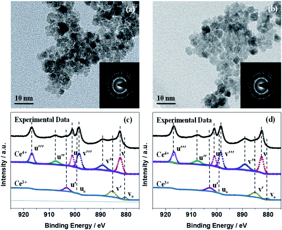 | ||
| Fig. 2 (a) TEM image before UV–O3 treatment. (b) TEM image after UV–O3 treatment. (c) XPS spectra before UV–O3 treatment. (d) XPS spectra after UV–O3 treatment. Insets of (a) and (b) are the corresponding SAEDs. | ||
X-ray photoelectron spectroscopy (XPS) measurements were used to confirm the composition of the CeOx film, as depicted in Fig. 2c and d. The XPS survey scans (Fig. S4†) showed the elemental spectra of Ce, O, and C, and the adventitious C was used as the charge reference. According to an equation reported in the literature (Fig. S4†),37,38 the concentration of Ce3+ was deduced from the Ce 3d spectra of the CeOx films obtained without and with UV–O3 treatment to be 0.27 and 0.21 (Fig. 2c and d), based on which the x values in the obtained CeOx samples were calculated as 1.86 and 1.89, respectively. As far as variation in the elemental composition is concerned, the contents of Ce3+ and Ce4+ in the UV–O3 treated CeOx film were similar to those in the film prepared without the treatment.
The structural, optical and electrical properties of the CeOx films were systematically studied to decide the aptness of CeOx as an ETL in PSCs. In general, the UV–O3 treatment is vital to get rid of the remaining solvents and enhance the properties of the CeOx films.32,39 The UV–O3-processed CeOx ETLs showed higher transmittance from 400 to 800 nm. As depicted in Fig. 3a, the optical transmittance of the CeOx ETLs gradually enhanced with an increase in thickness up to 6 spin-coating cycles (71 nm). This is likely owing to the reduction in the surface roughness of the CeOx ETLs coated on the PEN/ITO substrates relative to that of the bare PEN/ITO substrate. The top-view scanning electron microscopy (SEM) images showed a homogeneous integrated dense film on the ITO/PEN substrate spin-coated with the CeOx sol–gel, as seen in Fig. S3.† The compact pinhole-free CeOx films were successfully fabricated by 6 cycles of spin-coating under a UV–O3 atmosphere, which was in favor of improving the electron transport ability and increasing the perovskite deposition quantity between particles in the mesoporous framework. The current density versus voltage (J–V) characteristics were analyzed to investigate the impact of the UV–O3 treatment on electrical conductivity. The electrical conductivity of the UV/LT-CeOx film was 1.38 × 10⁻⁴ S cm−1, which was more than twice as that of the LT-CeOx film (0.65 × 10⁻⁴ S cm−1), due to the increased carrier density caused by the UV–O3 treatment.40,41 Noticeably, the UV-CeOx film (1.04 × 10⁻⁴ S cm−1) also exhibited higher conductivity than the LT-CeOx film. This is because the UV–O3 treatment hastened the disintegration of the stable surface groups and improved the links between the CeOx nanoparticles (Fig. 3b), as well as charge transport. Meanwhile, the UV–O3-induced epitaxial attachment of the CeOx nanocrystals in our study was similar to that reported by Hiraide et al.42
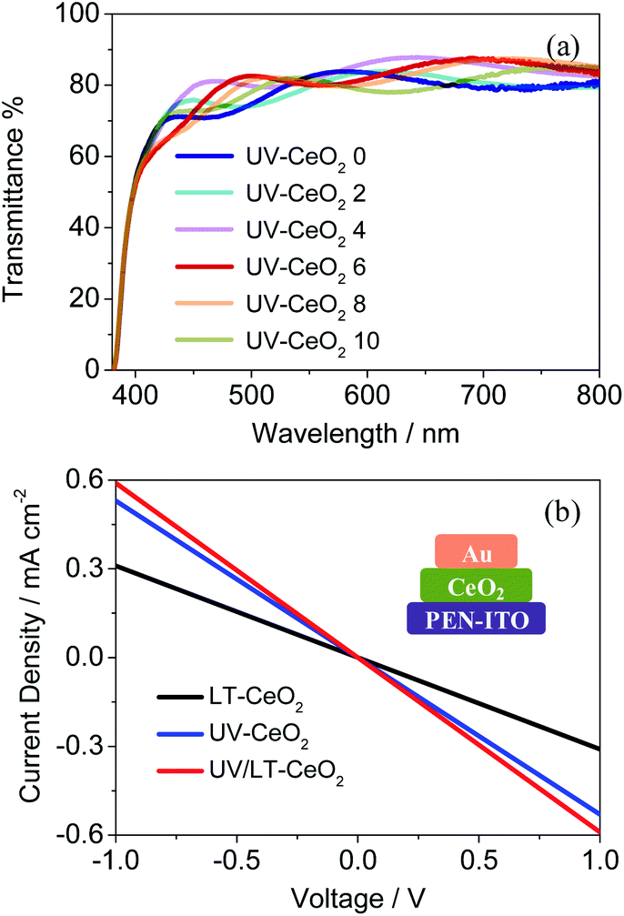 | ||
| Fig. 3 (a) Transmittance spectra of the CeOx films with different thicknesses. The number after “CeOx” in the legend indicates the number of CeOx ETLs spin-coated on the substrate. (b) Conductivity of the CeOx films produced using different treatment methods. | ||
The relationship between the thickness of the CeOx ETL and the photovoltaic performance is illustrated in Fig. S5.†Jsc and Voc initially enhanced as the film thickness increased, while they decreased beyond a certain film thickness. This result showed that the generation of photocurrent in CeOx PSCs would be dominated by high-quality ETLs below ca. 70 nm. To understand the electron transfer pathway in CeOx ETL, ultraviolet photoelectron spectra (UPS) and UV-vis absorbance spectra were obtained to establish the energy levels (Fig. S6†). The architecture and energy-level diagram of the CeOx-based f-PSCs are illustrated in Fig. S7.† Therefore, planar f-PSCs based on the LT-CeOx, UV-CeOx and UV/LT-CeOx ETLs were fabricated to explore their photovoltaic performance. As we know, good-quality perovskite films are key to highly-efficient stable PSCs. We prepared good quality CH3NH3PbI3 layers on different ETLs by adopting the Lewis-base adduct approach,43 which showed no effect on the perovskite morphology. The cross-sectional SEM image in Fig. 4a shows the device composed of typical perovskite layers: FTO/UV-CeOx ETL (70 nm)/CH3NH3PbI3 (480 nm)/spiro-OMeTAD (180 nm)/Au (88 nm). Fig. 4b exhibits the typical current density–voltage (J–V) curves of the cells built with the LT-CeOx, UV-CeOx, and UV/LT-CeOx ETLs. The ETL dependence of various photovoltaic parameters of the solar cells is listed in Table 1. The devices based on the LT-CeOx ETLs prepared at 80 °C exhibited a Jsc of 15.81 mA cm−2, a Voc of 0.92 V, a fill factor (FF) of 0.62, and PCE of 9.08%. In contrast, the PSCs based on the UV-CeOx ETLs exhibited distinctly advantageous performance with a Jsc of 18.78 mA cm−2, a Voc of 0.94, an FF of 0.69, and PCE of 12.21%. When the CeOx ETLs prepared at low temperature were irradiated by UV–O3 treatment, the corresponding UV/LT-CeOx-based PSCs showed remarkably higher characteristic factors with a Jsc of 19.42 mA cm−2, a Voc of 0.98 V, an FF of 0.72, and the best PCE at 14.63%. The extensive performance statistics for ca. 75 devices in each group can be found in Fig. S8.† The reasons for the improved performance of the UV/LT-CeOx devices than the LT-CeOx ones are better transparency, advantageous electrochemical properties, and the higher hole-blocking effect, which may be due to the decreased charge recombination since the UV–O3 treatment optimizes the defects sites on the CeOx film surface.44,45Fig. 4c illustrates the incident photon-to-current efficiency (IPCE) spectra of the cells. Compared with devices based on UV-CeOx and LT-CeOx, the broad spectral response (300–760 nm) of the UV/LT-CeOx devices exhibited a higher IPCE value dependence, which was devoted to the exceptional optical transparency and electrical conductivity of the CeOx ETL. The ratio of the respective integrated IPCE spectra of each batch corresponded with the ratio of the photocurrents.
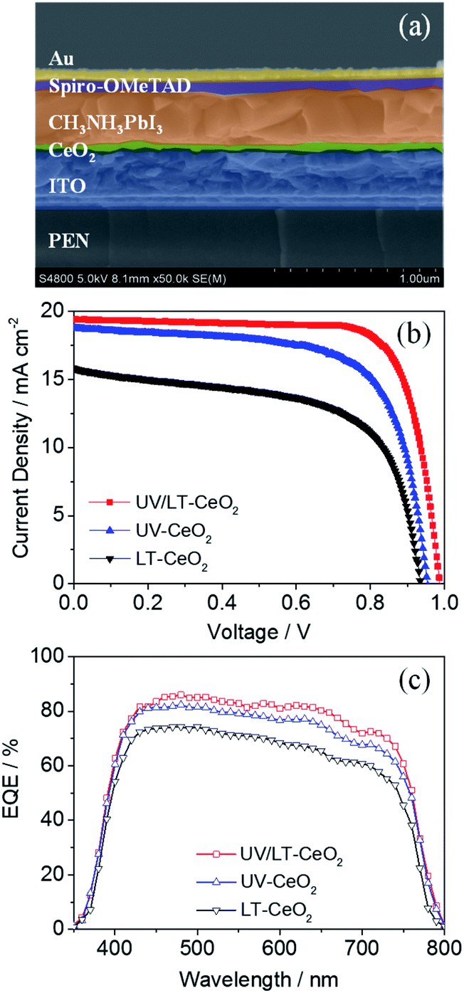 | ||
| Fig. 4 (a) Cross-sectional SEM image of the f-PSC based on the UV/LT-CeOx ETL. (b) J–V curves and (c) IPCE spectra of the high-performing f-PSCs fabricated with the LT-CeOx, UV-CeOx, and UV/LT-CeOx ETLs. | ||
| Sample | J sc/mA cm−2 | V oc/V | FF/% | PCE/% |
|---|---|---|---|---|
| a Max and avg represent the best and the average devices, respectively. | ||||
| LT-CeOx-max | 15.81 | 0.92 | 62.19 | 9.08 |
| LT-CeOx-avg | 15.93 | 0.91 | 58.72 | 8.49 |
| UV-CeOx-max | 18.78 | 0.94 | 69.31 | 12.21 |
| UV-CeOx-avg | 17.75 | 0.93 | 69.89 | 11.56 |
| UV/LT-CeOx-max | 19.42 | 0.98 | 76.21 | 14.63 |
| UV/LT-CeOx-avg | 19.01 | 0.96 | 74.38 | 13.50 |
To investigate the effect of doping UV–O3 in detail, PL and TRPL spectroscopy were performed to probe the charge transfer process between the CeOx ETL and the perovskite layer after UV–O3 doping. Fig. 5a exhibits that the quenching of the intrinsic CH3NH3PbI3 fluorescence emission by the ETLs occurred at the spectral peak (766 nm). Compared with the LT-CeOx/perovskite sample, the PL intensities of UV-CeOx/perovskite and UV/LT-CeOx/perovskite were drastically reduced with the UV–O3 doping process, indicating that the photocurrent density and recombination rate reduction were the most efficient in the UV–O3-processed ETLs. A higher increase in amplitude accompanied by a slow PL quenching, produced in a progressive manner from the perovskite and its interfaces. Therefore, the UV–O3 doping process is beneficial for speedy charge transport and enhanced charge generation and collection in the device. Fig. 5b presents the TRPL spectra and the matching PL decay times evaluated using an apparently bi-exponential decay model. The results for the LT-CeOx/perovskite, UV-CeOx/perovskite and UV/LT-CeOx/perovskite samples are summarized in Table S1.† The fast decay corresponded to the quenching of carriers from the perovskite layer to the ETLs, and the slow decay was regarded as the result of irradiative decay within the perovskite film.31,46,47 In comparison with the LT-CeOx film, the UV-CeOx ETL-based devices exhibited a fast decay constant decay, which dominated the charge extraction from the perovskite to the ETLs. The average lifetime at the interface between LT-CeOx and the perovskite film was 31.20 ns, which severely decreased to 26.11 ns at the interface between UV-CeOx and the perovskite film. In comparison with UV-CeOx/perovskite, a faster decay component could be observed at the UV/LT-CeOx/perovskite interface under increased amplitude (2.68 ns to 1.80 ns), which induced a low average lifetime (18.21 ns). Thus, the UPS spectra (Fig. S6b†) and PL emission spectra exhibited that charge transport and extraction were strongly enhanced by the synergistic effects of the sharp-shift in the energy level and the raised electrical conductivity, resulting in great enhancement of the photocurrent efficiency of the UV/LT-CeOx ETL.
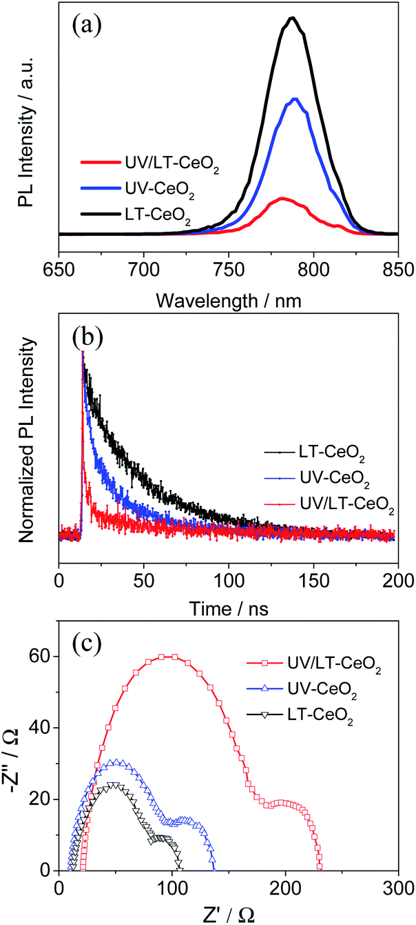 | ||
| Fig. 5 (a) Normalized steady-state photoluminescence (PL) spectra, (b) normalized time-resolved photoluminescence (TRPL) spectra and (c) EIS spectra of the LT-CeOx, UV-CeOx, and UV/LT-CeOx ETLs in PSCs. | ||
To further comprehend the improvement in performance upon UV–O3 treatment, electrochemical impedance spectroscopy (EIS) measurements were carried out on different devices since it is considered as an effective method to investigate the carrier transport behavior and interfacial properties of PSCs.48,49 The Nyquist plots displayed in Fig. 5c were obtained under dark at an applied bias voltage of 0.7 V in the frequency range from 0.1 to 100 kHz, in which two different semicircles are shown in the high- and low-frequency ranges. The Nyquist plots were fitted with an equivalent circuit containing a series resistance (Rs) in series with two RC elements. The fitted transport resistance (Rco) and recombination resistance (Rrec) were plotted in connection with UV–O3 and thermal treatments, as illustrated in Fig. S9 and Table S2.†50,51 When the CeOx film was treated at 80 °C, the water molecules in the ETLs could not be effectively removed to obtain ideal transmission resistance (LT-CeOx: Rco = 116.5 Ω cm2). In contrast, upon UV–O3 treatment, the Rco decreased significantly (Rco = 102.4 Ω cm2 for the UV-CeOx film and 87.8 Ω cm2 for the UV/LT-CeOx film), which is in accordance with the conductivity measurements (Fig. 3b). Moreover, compared with the Rrec of the LT-CeOx-based interfaces (336.2 Ω cm2), the Rrec of the UV-CeOx-based interfaces had increased to 456.9 Ω cm2, and that of the UV/LT-CeOx-based interfaces increased to 573.6 Ω cm2. Undoubtedly, the UV–O3 treatment optimized the CeOx/perovskite interface for a large part and reduced the recombination rate significantly by increasing the Rrec. Therefore, UV–O3 treatment is conducive to realizing outstanding low-temperature CeOx ETLs and achieving high-performance perovskite devices.
The low-temperature-processed ETLs subjected to the UV process are highly desirable for constructing high-performance flexible PSCs. Highly densely-packed CeOx ETLs were effectively prepared on sputtered PEN/ITO substrates, and then typical devices with the ETL/CH3NH3PbI3/spiro-OMeTAD/Au configuration were consecutively fabricated by conventional methods. The photograph of the flexible CeOx-based PSC with UV–O3 treatment is shown in Fig. 6a. The hysteresis effect under different J–V scans directions or rates were exhibited in PSCs, especially n–i–p planar devices.52,53 It has been proposed in previous works that the hysteresis initiates from polarization caused by ferroelectricity, ion motion of perovskite materials, and an unbalanced flux carrier density.54,55 As shown in Fig. 6b, we discovered that the devices based on the LT-CeOx ETL showed large hysteresis between the forward and reverse scanning directions. Nevertheless, this hysteresis behavior was greatly lessened in the UV-CeOx ETL devices, and the UV/LT-CeOx ETL-based ones illustrated the smallest hysteresis among the devices. This phenomenon most likely stemmed from the reduced accumulation of interfacial charge in the UV/LT-CeOx/perovskite interface. This result is consistent with the current hysteresis and photovoltaic performance. That is, the higher the charge extraction efficiency of selective contact, the lesser is the current hysteresis in the J–V curves, and the higher is the photovoltaic performance of the f-PSC. The stabilized photocurrents of the devices at 0.88 V bias under 1 sun illumination are tracked in Fig. S10a,† and the stabilized PCEs at the different bending radii of 15, 7 and 4 mm reached 13.96, 11.95 and 10.71% at 200 s continuous irradiation, respectively, as indicated in Fig. S10b.† To assess the stability of the devices with and without UV–O3 treatment, the long-term stability of cells stored in the air with 10% RH at 25 °C without packing was compared. The PCEs of the devices fabricated with UV/LT, UV and LT ETLs were measured continuously for 550 h. As presented in Fig. S10c,† the half-life of the device treated with UV/LT was at least 200 h longer than the other two half-life periods. This might be due to the compact perovskite film with a low trap-state density, which could effectively resist moisture penetration. Fig. 6c shows the J–V curves of the f-PSC as a function of the bending curvature radius and bending cycles. The remarkable PCE of the f-PSC was 14.63%. After 500 bending cycles at r = 15, 7 and 4 mm, the PCE values were 13.27%, 8.53% and 4.41%, respectively. These results illustrated that the initial efficiency was reduced to ca. 90% at r = 15 mm, but was caused devastating at r = 4 mm. We can assume that the slight decrease in PCE at r = 15 mm was due to the plastic deformation of the ITO/PEN substrate. However, the brittle ITO could possibly have broken when bent at r = 4 mm, which is consistent with previous reports.56,57 Meanwhile, the photovoltaic parameters (Jsc, Voc, and FF) showed an almost similar decreased tendency with a 2% loss after 500 bending cycles. Hence, we could conclude that the structure of the cell with r = 15 mm possessed outstanding mechanical durability. The durability test was also performed on the three devices at r = 15, 7 and 4 mm, for up to 500 cycles (Fig. S10d†). When the device was deformed once, the device performance decreased linearly at the same bending radius. The cells bent at 15 mm showed excellent stability with less than 10% reduction of the PCE after repeated bending at ambient temperature.
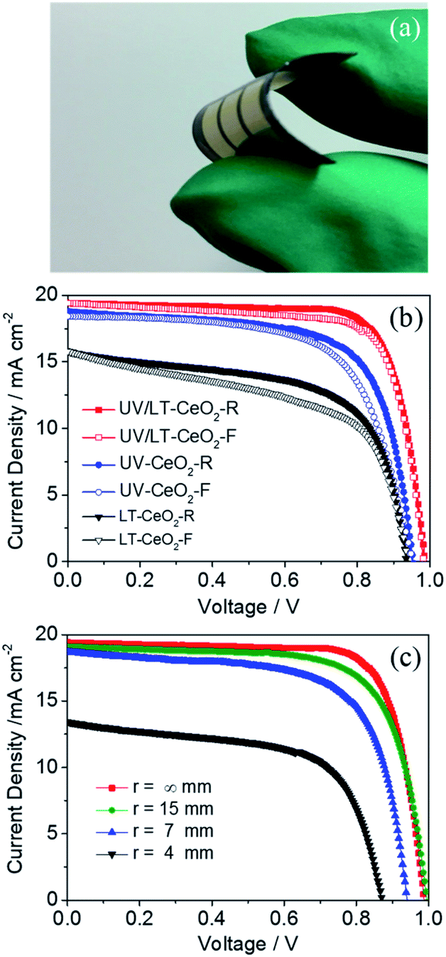 | ||
| Fig. 6 (a) Photograph of the f-PSC. (b) Hysteresis behavior of the f-PSCs based on the LT-CeOx, UV-CeOx, and UV/LT-CeOx ETLs, where F indicates the forward scan and R indicates the reverse scan in the J–V curves. (c) J–V curves of the f-PSCs with various radii (r) after recovery from 500 bending cycles. | ||
4. Conclusions
In this work, a low-temperature process (80 °C) for preparing highly efficient f-PSCs involving UV–O3 treatment of ligand-capped CeOx NCs was developed. The photocatalytic decomposition of the organic ligands accompanied the spontaneous coalescence of the NCs, resulting in highly efficient ETLs, which exhibited high performance, including high film compactness, high electrical conductivity, and high transparency, as well as favorable energy levels matching with the perovskite. Using the UV–O3 treated CeOx ETLs prepared at a low temperature, highly efficient planar PSCs with the best PCE of 14.63% was achieved with ITO/PEN substrates. We report a facile route that is very appropriate for the construction of high-performance f-PSCs because it easily modifies the ETLs at a low-temperature. This approach will pave the way for further development of f-PSCs and is feasible for large-scale roll-to-roll processes.Conflicts of interest
The authors declare no competing financial and nonfinancial interests.Acknowledgements
This work was financially supported by National Natural Science Foundation of China (21603230, 21073039 and 21801242), the CAS/SAFEA International Partnership Program for Creative Research Teams, the Strategic Priority Research Program of the Chinese Academy of Sciences (XDB20000000), and Key Laboratory of Novel Thin Film Solar Cells, CAS.References
- J. Burschka, N. Pellet, S. J. Moon, R. H. Baker, P. Gao, M. K. Nazeeruddin and M. Grätzel, Nature, 2013, 499, 316–319 CrossRef CAS PubMed.
- S. H. Turren-Cruz, A. Hagfeldt and M. Saliba, Science, 2018, 362, 449–453 CrossRef CAS PubMed.
- P. B. Ru, E. B. Bi, Y. Zhang, Y. B. Wang, W. Y. Kong, Y. M. Sha, W. T. Tang, P. Zhang, Y. Z. Wu, W. Chen, X. D. Yang, H. Chen and L. Y. Han, Adv. Energy Mater., 2020, 1903487, 1–9 Search PubMed.
- C. C. Wu, D. Wang, Y. Q. Zhang, F. D. Gu, G. H. Liu, N. Zhu, W. Luo, D. Han, X. Guo, B. Qu, S. F. Wang, Z. Q. Bian, Z. J. Chen and L. X. Xiao, Adv. Funct. Mater., 2019, 1902974, 1–7 Search PubMed.
- K. Q. Huang, Y. Y. Peng, Y. X. Gao, J. Shi, H. Y. Li, X. D. Mo, H. Huang, Y. L. Gao, L. M. Ding and J. L. Yang, Adv. Energy Mater., 2019, 1901419, 1–9 Search PubMed.
- M. M. Lee, J. Teuscher, T. Miyasaka, T. N. Murakami and H. J. Snaith, Science, 2012, 338, 643–647 CrossRef CAS PubMed.
- W. S. Yang, J. H. Noh, N. J. Jeon, Y. C. Kim, S. Ryu, J. Seo and S. I. Seok, Science, 2015, 348, 1234–1237 CrossRef CAS PubMed.
- F. D. Giacomo, V. Zardetto, A. D'Epifanio, S. Pescetelli, F. Matteocci, S. Razza, A. D. Carlo, S. Licoccia, W. M. M. Kessels, M. Creatore and T. M. Brown, Adv. Energy Mater., 2015, 5, 1401808 CrossRef.
- I. Jeong, H. Jung, M. Park, J. S. Park, H. J. Son, J. Joo, J. Lee and M. J. Ko, Nano Energy, 2016, 28, 380–389 CrossRef CAS.
- U. Ryu, S. Jee, J. Park, K. Han, J. H. Lee, M. Park and K. M. Choi, ACS Nano, 2018, 12, 4968–4975 CrossRef CAS PubMed.
- M. Lee, Y. Jo, D. S. Kim, H. Y. Jeong and Y. Jun, J. Mater. Chem. A, 2015, 3, 14592–14597 RSC.
- C. Tao, S. Neutzner, L. Colella, S. Marras, A. R. S. Kandada, M. Gandini, M. D. Bastiani, G. Pace, L. Manna, M. Caironi, C. Bertarelli and A. Petrozza, Energy Environ. Sci., 2015, 8, 2365–2370 RSC.
- T. Leijtens, G. E. Eperon, S. Pathak, A. Abate, M. M. Lee and H. J. Snaith, Nat. Commun., 2013, 4, 3885 Search PubMed.
- W. Li, W. Zhang, S. V. Reenen, R. J. Sutton, J. Fan, A. A. Haghighirad, M. B. Johnston, L. Wang and H. J. Snaith, Energy Environ. Sci., 2016, 9, 490–498 RSC.
- P. P. Boix, K. Nonomura, N. Mathews and S. G. Mhaisalkar, Mater. Today, 2014, 17, 16–23 CrossRef CAS.
- D. Q. Bi, G. Boschloo, S. Schwarzmuller, L. Yang, E. M. J. Johansson and A. Hagfeldt, Nanoscale, 2013, 5, 11686–11691 RSC.
- K. Hwang, Y. S. Jung, Y. J. Heo, F. H. Scholes, S. E. Watkins, J. Subbiah, D. J. Jones, D. Y. Kim and D. Vak, Adv. Mater., 2015, 27, 1241–1247 CrossRef CAS PubMed.
- Y. Yang, J. You, Z. Hong, Q. Chen, M. Cai, T. B. Song, C. C. Chen, S. Lu, Y. Liu and H. Zhou, ACS Nano, 2014, 8, 1674–1680 CrossRef PubMed.
- J. H. Heo, M. H. Lee, H. J. Han, B. R. Patil, J. S. Yu and S. H. Im, J. Mater. Chem. A, 2016, 4, 1572–1578 RSC.
- J. Yang, B. D. Siempelkamp, E. Mosconi, F. D. Angelis and T. L. Kelly, Chem. Mater., 2015, 27, 4229–4236 CrossRef CAS.
- Y. Cheng, Q. D. Yang, J. Xiao, Q. Xue, H. W. Li, Z. Guan, H. L. Yip and S. W. Tsang, ACS Appl. Mater. Interfaces, 2015, 7, 19986–19993 CrossRef PubMed.
- Q. Wali, A. Fakharuddin, I. Ahmed, M. H. Ab Rahim, J. Ismail and R. Jose, J. Mater. Chem. A, 2014, 2, 17427–17434 RSC.
- Q. Jiang, L. Zhang, H. Wang, X. Yang, J. Meng, H. Liu, Z. Yin, J. Wu, X. Zhang and J. You, Nat. Energy, 2016, 2, 16177 CrossRef.
- W. Ke, G. Fang, Q. Liu, L. Xiong, P. Qin, H. Tao, J. Wang, H. Lei, B. Li, J. Wan, G. Yang and Y. Yan, J. Am. Chem. Soc., 2015, 137, 6730–6733 CrossRef CAS PubMed.
- J. P. Correa Baena, L. Steier, W. Tress, M. Saliba, S. Neutzner, T. Matsui, F. Giordano, T. J. Jacobsson, A. R. Srimath Kandada, S. M. Zakeeruddin, A. Petrozza, A. Abate, M. K. Nazeeruddin, M. Grätzel and A. Hagfeldt, Energy Environ. Sci., 2015, 8, 2928–2934 RSC.
- C. Wang, D. Zhao, C. R. Grice, W. Liao, Y. Yu, A. Cimaroli, N. Shrestha, P. J. Roland, J. Chen, Z. Yu, P. Liu, N. Cheng, R. J. Ellingson, X. Zhao and Y. Yan, J. Mater. Chem. A, 2016, 4, 12080–12087 RSC.
- A. Corma, P. Atienzar, H. García and J. Y. C. Ching, Nat. Mater., 2004, 3, 394–397 CrossRef CAS PubMed.
- R. Jose, V. Thavasi and S. Ramakrishna, J. Am. Ceram. Soc., 2009, 92, 289–301 CrossRef CAS.
- X. Wang, L. L. Deng, L. Y. Wang, S. M. Dai, Z. Xing, X. X. Zhan, X. Z. Lu, S. Y. Xie, R. B. Huang and L. S. Zheng, J. Mater. Chem. A, 2017, 5, 1706–1712 RSC.
- T. Hu, S. Q. Xiao, H. J. Yang, L. Chen and Y. W. Chen, Chem. Commun., 2018, 54, 471–474 RSC.
- P. Periyat, F. Laffir, S. A. M. Tofaila and E. Magner, RSC Adv., 2011, 1, 1794–1798 RSC.
- A. Y. Pang, D. L. Shen, M. D. Wei and Z. N. Chen, ChemSusChem, 2018, 11, 424–431 CrossRef CAS PubMed.
- S. C. Pillai, P. Periyat, R. G. Kutty, D. E. McCormack, M. K. Seery, H. Hayden, J. Colreavy, D. Corr and S. J. Hinder, J. Phys. Chem. C, 2007, 111, 1605–1611 CrossRef CAS.
- L. Ren, X. Huang, F. Sun and X. He, Mater. Lett., 2007, 61, 427–431 CrossRef CAS.
- H. Gu and M. D. Soucek, Chem. Mater., 2007, 19, 1103–1110 CrossRef CAS.
- Z. A. Tan, L. Li, C. Li, L. Yan, F. Wang, J. Xu, L. Yu, B. Song, J. Hou and Y. Li, Adv. Mater. Interfaces, 2014, 1, 1400197 CrossRef.
- S. Watanabe, X. Ma and C. Song, J. Phys. Chem. C, 2009, 113, 14249–14257 CrossRef CAS.
- K. H. Jung, J. Y. Seo, S. Lee, H. Shin and N. G. Park, J. Mater. Chem. A, 2017, 5, 24790–24803 RSC.
- W. Ke, D. Zhao, A. J. Cimaroli, C. R. Grice, P. Qin, Q. Liu, L. Xiong, Y. Yan and G. Fang, J. Mater. Chem. A, 2015, 3, 24163–24168 RSC.
- T. Nikolay, L. Larina, O. Shevaleevskiy and B. T. Ahn, Energy Environ. Sci., 2011, 4, 1480–1486 RSC.
- W. Chen, Y. Wu, Y. Yue, J. Liu, W. Zhang, X. Yang, H. Chen, E. Bi, I. Ashraful, M. Grätzel and L. Han, Science, 2015, 350, 944–948 CrossRef CAS PubMed.
- T. Hiraide, H. Kageyama, Y. Nakagawa, Y. Oaki and H. Imai, Chem. Commun., 2016, 52, 7545–7548 RSC.
- N. Ahn, D. Y. Son, I. H. Jang, S. M. Kang, M. Choi and N. G. Park, J. Am. Chem. Soc., 2015, 137, 8696–8799 CrossRef CAS PubMed.
- D. H. Kim, G. S. Han, W. M. Seong, J. W. Lee, B. J. Kim, N. G. Park, K. S. Hong, S. Lee and H. S. Jung, ChemSusChem, 2015, 8, 2392–2398 CrossRef CAS PubMed.
- X. Lü, X. Mou, J. Wu, D. Zhang, L. Zhang, F. Huang, F. Xu and S. Huang, Adv. Funct. Mater., 2010, 20, 509–515 CrossRef.
- G. Niu, W. Li, F. Meng, L. Wang, H. Dong and Y. Qiu, J. Mater. Chem. A, 2014, 2, 705–710 RSC.
- B. Duan, Y. K. Ren, Y. F. Xu, W. Y. Chen, Q. Ye, Y. Huang, J. Zhu and S. Y. Dai, Inorg. Chem. Front., 2017, 4, 473–480 RSC.
- T. Bu, L. Wu, X. Liu, X. Yang, P. Zhou, X. Yu, T. Qin, J. Shi, S. Wang, S. Li, Z. Ku, Y. Peng, F. Huang, Q. Meng, Y. B. Cheng and J. Zhong, Adv. Energy Mater., 2017, 7, 1700576 CrossRef.
- I. Zarazua, G. Han, P. P. Boix, S. Mhaisalkar, F. FabregatSantiago, I. Mora-Sero, J. Bisquert and G. Garcia-Belmonte, J. Phys. Chem. Lett., 2016, 7, 5105–5113 CrossRef CAS PubMed.
- J. Dagar, S. Castro-Hermosa, M. Gasbarri, A. L. Palma, L. Cina, F. Matteocci, E. Calabro, A. D. Carlo and T. M. Brown, Nano Res., 2018, 11, 2669–2681 CrossRef CAS.
- T. Bu, S. W. Shi, J. Li, Y. F. Liu, J. L. Shi, L. Chen, X. P. Liu, J. H. Qiu, Z. L. Ku, Y. Peng, J. Zhong, Y. B. Cheng and F. Z. Huang, ACS Appl. Mater. Interfaces, 2018, 10, 14922–14929 CrossRef CAS PubMed.
- H. J. Snaith, A. Abate, J. M. Ball, G. E. Eperon, T. Leijtens, N. K. Noel, S. D. Stranks, J. T. W. Wang, K. Wojciechowski and W. Zhang, J. Phys. Chem. Lett., 2014, 5, 1511–1515 CrossRef CAS PubMed.
- J. H. Heo, H. J. Han, D. Kim, T. K. Ahn and S. H. Im, Energy Environ. Sci., 2015, 8, 1602–1608 RSC.
- Y. Shao, Z. Xiao, C. Bi, Y. Yuan and J. Huang, Nat. Commun., 2014, 5, 5784 CrossRef CAS PubMed.
- C. Li, S. Tscheuschner, F. Paulus, P. E. Hopkinson, J. Kießling, A. Köhler, Y. Vaynzof and S. Huettner, Adv. Mater., 2016, 28, 2446–2454 CrossRef CAS PubMed.
- B. J. Kim, D. H. Kim, Y. Y. Lee, H. W. Shin, G. S. Han, J. S. Hong, K. Mahmood, T. K. Ahn, Y. C. Joo, K. S. Hong, N. G. Park, S. Lee and H. S. Jung, Energy Environ. Sci., 2015, 8, 916–921 RSC.
- J. W. Jo, M. S. Seo, M. Park, J. Y. Kim, J. S. Park, I. K. Han, H. Ahn, J. W. Jung, B. H. Sohn, M. J. Ko and H. J. Son, Adv. Funct. Mater., 2016, 26, 4464–4471 CrossRef CAS.
Footnote |
| † Electronic supplementary information (ESI) available. See DOI: 10.1039/d0na00367k |
| This journal is © The Royal Society of Chemistry 2020 |