 Open Access Article
Atomically thin heavy-metal-free ZnTe nanoplatelets formed from magic-size nanoclusters†
Fei
Wang
a,
Minyi
Zhang
b,
Wei
Chen
 a,
Shaghraf
Javaid
 a,
Heng
Yang
c,
Sheng
Wang
c,
Xuyong
Yang
 c,
Lai-Chang
Zhang
d,
Mark A.
Buntine
a,
Chunsen
Li
 *b and
Guohua
Jia
*a
aCurtin Institute of Functional Molecules and Interfaces, School of Molecular and Life Science, Curtin University, Bentley, WA 6102, Australia. E-mail: guohua.jia@curtin.edu.au
bState Key Laboratory of Structural Chemistry, Fujian Institute of Research on the Structure of Matter, Chinese Academy of Sciences, Fuzhou, Fujian 350002, China. E-mail: chunsen.li@fjirsm.ac.cn
cKey Laboratory of Advanced Display and System Applications of Ministry of Education, Shanghai University, 149 Yanchang Road, Shanghai 200072, P. R. China
dSchool of Engineering, Edith Cowan University, 270 Joondalup Drive, Joondalup, WA 6027, Australia
First published on 27th May 2020
Abstract
Atomically thin colloidal quasi-two-dimensional (2D) semiconductor nanoplatelets (NPLs) have attracted tremendous attention due to their excellent properties and stimulating applications. Although some advances have been achieved in Cd- and Pb-based semiconductor NPLs, research into heavy-metal-free NPLs has been reported less due to the difficulties in the synthesis and the knowledge gap in the understanding of the growth mechanism. Herein wurtzite ZnTe NPLs with an atomic thickness of about 1.5 nm have been successfully synthesized by using Superhydride (LiEt3BH) reduced tributylphosphine–Te (TBP-Te) as the tellurium precursor. Mechanistic studies, both experimentally and theoretically, elucidate the transformation from metastable ZnTe MSC-323 magic-size nanoclusters (MSCs) to metastable ZnTe MSC-398, which then forms wurtzite ZnTe NPLs via an oriented attachment mechanism along the [100] and [002] directions of the wurtzite structure. This work not only provides insightful views into the growth mechanism of 2D NPLs but also opens an avenue for their applications in optoelectronics.
Introduction
Over the past ten years, colloidal semiconductor NPLs with a few layers of atomic thickness1–4 have been of great interest due to their exceptional photophysical properties such as a short PL lifetime,5 extremely narrow PL linewidth,6 low lasing threshold,4 and giant oscillator strength.7 Unlike the synthesis of zinc-blende II–VI NPLs in 1-octadecene (ODE), which combines fatty acid salts with fatty acids as the cation precursor solution at elevated temperatures,8–11 wurtzite II–VI colloidal NPLs were proposed to evolve from MSCs as intermediate synthons within soft colloidal templates at mild reaction temperatures.1,12–14 Currently, the majority of II–VI colloidal nanoplatelets with wurtzite or zinc-blende structures are based on cadmium chalcogenides. The toxicity of materials and government regulations, however, hinder the widespread use of heavy metals, especially semiconductor nanocrystals containing cadmium. Potential alternatives to these toxic materials are heavy-metal free zinc chalcogenide semiconductor nanocrystals because they are environmentally benign and earth-abundant materials.15–20Among ZnX (X = S, Se, and Te) semiconductors, ZnTe with a direct bandgap of 2.26 eV in bulk and excellent physical properties, such as ultrafast charge separation and transfer dynamics, has important applications such as in photodetectors,21 solar cells,22 and terahertz imaging.23 Although bulk ZnTe materials are stable under ambient conditions, their counterparts such as ZnTe nanocrystals are extremely vulnerable to air and moisture and tend to undergo decomposition as they have a large number of surface atoms. This makes the study on ZnTe nanocrystals challenging because of the instability of ZnTe nanocrystals and the rigid oxygen- and moisture-free conditions required in post-synthesis handling. Furthermore, the chemistry of tellurium precursors is not well-developed and therefore substantial effort in this field is highly demanded.
Zhang et al. developed a synthetic approach for producing wurtzite ZnTe nanorods with a controllable aspect ratio by tuning the reaction temperature and time.24 In addition, they reported the self-assembly of ZnTe MSCs that evolved into one-dimensional (1D) wurtzite ZnTe ultrathin nanowires via alignment and fusion along the [002] crystallographic direction at a prolonged reaction time,25 which is different from the growth behaviour of CdSe MSCs as a nucleant for the growth of wurtzite CdSe NPLs.1,13,14 Hyeon et al. suggested that the growth of wurtzite CdSe NPLs preferred a mild reaction temperature because it can differentiate the subtle surface energy difference between (100) and (110) facets of the wurtzite structure, and also stabilize the MSCs and the soft colloidal templates.26 However, because of the metallic characteristics of both zinc and tellurium, a reaction for the synthesis of ZnTe nanocrystals conducted at a mild temperature may not be able to overcome the reaction activation energy barrier; therefore, tellurium precursors with appropriate reactivity are required. This suggests that care should be taken to keep the balance between the reactivity of tellurium precursors and the reaction temperature in the preparation of ZnTe nanocrystals with one-dimensional or two-dimensional shapes. Tellurium precursors such as bis(tert-butyldimethylsilyl) telluride,1 trioctylphosphine telluride (TOP-Te),27 polytellurides reduced from TOP-Te by Superhydride,24 tributylphosphine telluride (TBP-Te)28 and tris(dimethylamino)phosphine telluride29 were used to synthesize CdTe or ZnTe nanocrystals. For the synthesis conducted at a mild reaction temperature, high-quality ZnTe or CdTe nanocrystals can only be obtained by using tris(dimethylamino)phosphine telluride or polytellurides reduced from TOP-Te.
Herein we report the synthesis and growth mechanism of free-standing layered wurtzite ZnTe NPLs with a thickness of ∼1.5 nm by using Superhydride (LiEt3BH) reduced tributylphosphine-Te (TBP-Te) as the tellurium precursor. From both experimental and theoretical perspectives, we reveal that the growth mechanism of wurtzite ZnTe NPLs involves a stepwise transition from metastable self-assembled ZnTe MSC-323 to ZnTe MSC-398 and then oriented attachment of ZnTe MSC-398 along [100] and [002] directions to produce NPLs.
Experimental
Chemicals
Zinc chloride (99.999% trace metals basis), oleylamine (technical grade, 70%), dodecylamine (99%), tributylphosphine (mixture of isomers, 97%), Super-hydride® solution (1.0 M lithium triethylborohydride in THF), anhydrous hexane (95%), anhydrous toluene (99.8%), and anhydrous methanol (99.8%) were purchased from Sigma-Aldrich. Tellurium powder (∼325 mesh, 99.99% metals basis) was obtained from Alfa Aesar. CDCl3 (D, 99.8%) was purchased from Cambridge Isotope Laboratories, Inc. All the materials were used as received without further purification.Synthesis of 0.5 M tributylphosphine telluride (TBP-Te) stock solution
A clear and yellow TBP-Te stock solution (0.5 M) was prepared by heating 30 ml tributylphosphine (TBP) and 1.914 g (15 mmol) tellurium powder at 240 °C for 3 hours under a nitrogen atmosphere using the standard Schlenk line techniques.Synthesis of self-assembled ZnTe MSCs and ZnTe NPLs
In a 50 ml flask, 272 mg ZnCl2 (2 mmol), 3.224 g dodecylamine and 16 ml oleylamine were mixed and degassed at room temperature three times, and then the mixture was heated at 200 °C for an hour before cooling down to 60 °C under nitrogen for hot-injection of the tellurium precursor that was freshly prepared in a glove box by using 4 ml oleylamine, 2 ml TBP-Te stock solution (0.5 M) and 1.2 ml of Superhydride solution. After hot-injection, the reaction temperature was increased from 60 °C to 120 °C in 6 minutes. As the reaction mixture was maintained for 2 hours at 120 °C, the first aliquot was taken, which was the reaction product of self-assembled ZnTe MSC-323. Then the reaction temperature was further increased to 200 °C in 5 minutes. As the reaction proceeded at 200 °C for 2 minutes, the second aliquot was taken, which was the reaction product of self-assembled ZnTe MSC-398. After another 30 minutes, the reaction was stopped by removing the heating mantle and cooling it down to room temperature.Characterization
UV-Vis absorption spectra were recorded on a Cary 4000 UV-Vis spectrophotometer with a 1 nm resolution in a quartz cell with a 1 cm path length. Low-resolution transmission electron microscopy (TEM) and selected-area electron diffraction (SAED) were conducted using a JEOL 2100 transmission electron microscope with an accelerating voltage of 120 kV. The SAED pattern was fitted using PASAD tools for DigitalMicrograph. High-resolution TEM (HRTEM), high angle annular dark field-scanning transmission electron microscopy (HAADF-STEM) and STEM-energy-dispersive X-ray spectroscopy (STEM-EDX) were performed on a FEI Titan G2 80-200 transmission electron microscope operating at 200 kV. All the reaction products were purified in a glove box using anhydrous hexane or anhydrous toluene as the solvent and anhydrous methanol as the antisolvent. The reaction products were centrifuged at 6000 rpm/3 minutes for ZnTe MSC-323 and at 5000 rpm/3 minutes for ZnTe MSC-398 and ZnTe NPLs. The purification was repeated again and then the purified ZnTe MSCs and NPLs were redispersed into anhydrous toluene. Then a drop of the solution was added onto an ultra-thin carbon-coated copper grid and the grid with the nanocrystals was dried in a glove box. Nuclear magnetic resonance (NMR) samples of TBP-Te were prepared in CDCl3. 1H and 31P NMR spectra were recorded on a Bruker Avance III 500 MHz spectrometer.Results and discussion
The tellurium precursors were prepared by reducing the TBP-Te solution with Superhydride. The 1H chemical shift indicates that the H atoms in TBP and TBP-Te have different chemical environments, which is indirect evidence for the formation of TBP-P (Fig. S1†). The main resonance appearing at −30.8 ppm (upper curve in Fig. S7†) was from TBP in the absence of Te. The broad resonance at −24.7 ppm (bottom curve in Fig. S7†) was from the mixture of TBP-Te and TBP, which results from the fast exchange of Te between TBP-Te and TBP (Fig. S2†).Fig. 1 presents the absorption spectra of the aliquots taken at various reaction stages and clearly shows the sharp absorption peaks of ZnTe MSCs and NPLs. After hot-injection of the tellurium precursor at 60 °C, the temperature of the reaction mixture was increased to 120 °C in 6 minutes. The mild hot-injection temperature is necessary to stabilize the MSCs because we found that ZnTe MSCs were not produced if the injection temperature was higher than 60 °C. Some reactions may have already taken place at 60 °C,30,31 producing precursor compounds and monomers that are indispensable for the formation of MSC-323 at 120 °C.30,31
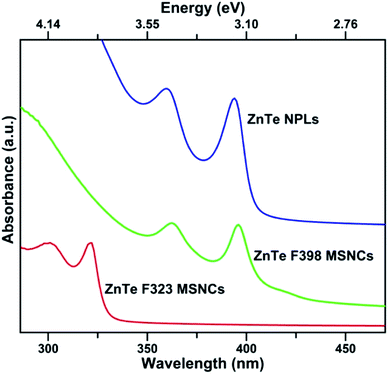 | ||
| Fig. 1 UV-Vis absorption spectra (red curve) of ZnTe MSC-323, ZnTe MSC-398 (green curve) and ZnTe NPLs (blue curve). | ||
The first aliquot was taken from the turbid white solution when the reaction proceeded for 2 hours at 120 °C. The corresponding absorption spectrum (red curve in Fig. 1) presents a sharp peak at 323 nm along with a shoulder at 297 nm, which matches well with the characteristic absorption peak locations of ZnTe MSC-323.25 Within 5 minutes, the reaction temperature further increased to 200 °C and the reaction mixture turned turbid and light-yellow gradually. As the reaction proceeded for 2 minutes at 200 °C, the second aliquot was taken and its absorption spectrum (green curve in Fig. 1) exhibits two peaks at 362 and 398 nm, matching the unique absorption peak locations of ZnTe MSC-398.25 As the reaction proceeded for 30 minutes at 200 °C, ZnTe NPLs were obtained and the exciton absorption peaks of ZnTe NPLs (blue curve in Fig. 1) appear at 360 and 396 nm. In addition, the first exciton absorption peak of ZnTe NPLs is much sharper than that of ZnTe MSC-398. Here, the “double absorption peaks” feature is usually observed for both zinc blende and wurtzite II–VI semiconductor nanoplatelets due to the electron-light hole (e-lh) and electron-heavy hole (e-hh) transitions.1,6,9
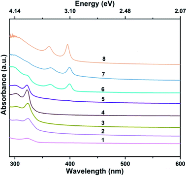
To analyse the transition from metastable ZnTe MSCs to ZnTe NPLs in detail, more aliquots were taken to investigate this process. The temporal evolution of the UV-Vis absorption spectra of the aliquots is compared in Fig. 2 as the reaction temperature increases from 120 °C to 200 °C. As the temperature increases to 120 °C, the absorption spectrum of the aliquot shows a broad peak at 325 nm (curve 1, Fig. 2). As the reaction evolves from 10 to 120 min at this temperature, this peak becomes sharper (curve 1–4, Fig. 2). The absorption spectrum (curve 4, Fig. 2) of ZnTe MSC-323 displays two distinctive exciton peaks at 302 nm and 323 nm. As the reaction temperature increases from 120 °C to 200 °C, the absorption peaks of ZnTe MSC-323 fade along with the appearance of the absorption peaks of ZnTe MSC-398 (curve 5 and 6, Fig. 2). The coincidence of the characteristic absorption features of both ZnTe MSC-323 and MSC-398 confirms the stepwise transition from metastable ZnTe MSC-323 to ZnTe MSC-398, which is similar to that observed in CdSe MSCs reported elsewhere.32 Interestingly, the exciton absorption peak of ZnTe NPLs (curve 8, Fig. 2) shows a slight blue shift of 2 nm with respect to that of ZnTe MSC-398 (curve 7, Fig. 2). This may indicate that ZnTe NPLs form an atomically flat basal plane; therefore the excitons are confined only in the thickness direction of ZnTe NPLs. Both ZnTe MSCs and NPLs do not have detectable PL, which results from surface traps and the dynamic nature of alkylamine ligands.33
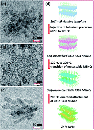
The TEM image of ZnTe MSC-323 (Fig. 3a) obtained at 120 °C for 120 minutes shows that the MSCs self-assembled in coin-like plates with a lateral size of ∼20 nm. Interestingly, these self-assembled MSCs (Fig. S5†) can stack with each other due to weak interactions between the bilayer mesophase template.1 As the reaction temperature increased from 120 °C to 200 °C and proceeded for 2 minutes at this temperature, the first exciton absorption peak has a profound red-shift from 323 nm to 398 nm (red and green curve in Fig. 1), which corresponds to the transition from metastable ZnTe MSC-323 to ZnTe MSC-398. This suggests that the increase of the reaction temperature broke the structural stability of metastable self-assembled ZnTe MSC-323 and resulted in the formation of ZnTe MSC-398 from the transition of self-assembled ZnTe MSC-323. Our observation showed that the transition from MSC-323 to MSC-398 manifesting a significant red shift of the absorption onset could be induced by a kinetics driven reconstruction of self-assembled MSC-323.
Fig. 3b presents the TEM image of self-assembled ZnTe MSC-398 with an irregular plate-like shape. In addition, the high-angle annular dark-field scanning transmission electron microscopy (HAADF-STEM) image (Fig. S6†) reveals that this self-assembled ZnTe MSC-398 was composed of individual small particles, being similar to those reported by Zhang et al.25 After the reaction proceeded for 30 minutes at 200 °C, well-defined rectangle-shaped ZnTe NPLs (Fig. 3c) with lateral dimensions of ∼20 nm × ∼60 nm were formed. Fig. 3d presents a schematic illustration to summarise the synthesis of ZnTe NPLs converted from the stepwise transition of metastable self-assembled ZnTe MSC-323 and MSC-398.
Fig. 4a shows the TEM image of single-layered ZnTe NPLs. ZnTe NPLs with a two dimensional rectangular shape are observed alongside with black dots. These black dots are Te metal dots due to the oxidation of ZnTe NPLs. The high-resolution TEM (HRTEM) image (Fig. 4b), the Fast Fourier Transform (FFT) of the HRTEM image (Fig. 4c) and selected-area electron diffraction (SAED) pattern (Fig. 4d) of ZnTe NPLs reveal that ZnTe NPLs are single-crystalline with a hexagonal wurtzite structure. Lattice spacing values extracted from the FFT of the HRTEM image are 0.355 nm and 0.374 nm for (002) and (100) crystal facets, respectively, confirming that the long lateral direction of ZnTe NPLs corresponds to the c-axis of the wurtzite structure. To further analyze the crystal structure of the as-prepared ZnTe NPLs, the SAED pattern of ZnTe NPLs was resolved by using PASAD tools (Fig. S5†). The corresponding Miller indices were annotated to the diffraction peaks (Fig. S6†) according to the resolved lattice spacing values as listed in Table S1,† which confirms the as-prepared ZnTe NPLs with a wurtzite structure. The fitted lattice spacing values of ZnTe NPLs were a little bit smaller than the standard values for wurtzite bulk CdTe (JCPDS No. 19-1482), which results from the lattice contraction phenomenon that was also observed in CdSe nanosheets1 and CdTe quantum belts.14Fig. 4e shows that each ZnTe NPL stands on its edge. The thickness of a single ZnTe NPL is estimated to be ∼1.5 nm, which is close to the ∼1.4 nm thickness of ZnSe and CdSe nanosheets.1,34Fig. 4f–i present the HAADF-STEM image and the corresponding STEM-EDX elemental maps of ZnTe NPLs. The element maps show that the obtained NPLs contain both Zn and Te elements, with both elements being evenly distributed throughout the ZnTe NPLs. The elemental maps shown in Fig. 4i also confirm the formation of the Te metal dots, which is attributed to the oxidation of ZnTe NPLs during the preparation or purification or characterization of the TEM samples.
To elucidate the growth mechanism of wurtzite ZnTe NPLs, density functional theory (DFT) calculations were performed (see the ESI for more details†). We studied the surface energies of (110), (100) and (002)/(00![[2 with combining macron]](https://www.rsc.org/images/entities/char_0032_0304.gif) ) facets, which are relevant to the growth of wurtzite ZnTe NPLs. The (110), (100) and (002)/(00
) facets, which are relevant to the growth of wurtzite ZnTe NPLs. The (110), (100) and (002)/(00![[2 with combining macron]](https://www.rsc.org/images/entities/char_0032_0304.gif) ) terminated facets of wurtzite ZnTe NPLs are shown in Fig. S7.† The surface energy calculations show that the polar (002)/(00
) terminated facets of wurtzite ZnTe NPLs are shown in Fig. S7.† The surface energy calculations show that the polar (002)/(00![[2 with combining macron]](https://www.rsc.org/images/entities/char_0032_0304.gif) ) facets have significantly higher surface energy than any of the non-polar (110) and (100) facets over almost the entire thermodynamically allowed range (Fig. 5), being similar to other systems with a hexagonal wurtzite crystal structure.35 In this sense, fast growth or oriented-attachment of ZnTe nanocrystals or MSCs along polar [002]/[00
) facets have significantly higher surface energy than any of the non-polar (110) and (100) facets over almost the entire thermodynamically allowed range (Fig. 5), being similar to other systems with a hexagonal wurtzite crystal structure.35 In this sense, fast growth or oriented-attachment of ZnTe nanocrystals or MSCs along polar [002]/[00![[2 with combining macron]](https://www.rsc.org/images/entities/char_0032_0304.gif) ] directions is thermodynamically favoured, dominating the growth of wurtzite ZnTe NPLs. Since the surface energies of (110) and (100) facets are almost equal, the size difference between (110) and (100) facets of the as-synthesized wurtzite ZnTe NPLs cannot be explained.
] directions is thermodynamically favoured, dominating the growth of wurtzite ZnTe NPLs. Since the surface energies of (110) and (100) facets are almost equal, the size difference between (110) and (100) facets of the as-synthesized wurtzite ZnTe NPLs cannot be explained.
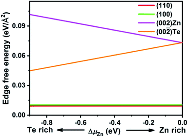 | ||
| Fig. 5 Surface energy as a function of the chemical potential ΔμZn of the wurtzite ZnTe slab surface. | ||
To further investigate the growth behaviour along [110] and [100] directions, we chose a wurtzite (ZnTe)34 MSC as a nucleate because the magic number 34 has been experimentally determined for other II–IV MSCs.14,36 Three isomers of (ZnTe)34 MSCs with a stacking morphology are shown in Fig. 6. Structure I in Fig. 6a presents a bilayer wurtzite stack which contains ten hexagonal rings and one complementary atom connecting two hexagonal edges on each layer with calculated energies of −69![[thin space (1/6-em)]](https://www.rsc.org/images/entities/char_2009.gif) 611.6675 a.u.; structure II in Fig. 6b also corresponds to the bilayer wurtzite stack with ten hexagons on each layer and a complementary atom connecting two hexagonal edges on each layer with calculated energies of −69
611.6675 a.u.; structure II in Fig. 6b also corresponds to the bilayer wurtzite stack with ten hexagons on each layer and a complementary atom connecting two hexagonal edges on each layer with calculated energies of −69![[thin space (1/6-em)]](https://www.rsc.org/images/entities/char_2009.gif) 611.6302 a.u.; structure III in Fig. 6c corresponds to a four-layer wurtzite stack with four hexagons on each layer and a complementary atom connecting two hexagonal edges on each layer with calculated energies of −69
611.6302 a.u.; structure III in Fig. 6c corresponds to a four-layer wurtzite stack with four hexagons on each layer and a complementary atom connecting two hexagonal edges on each layer with calculated energies of −69![[thin space (1/6-em)]](https://www.rsc.org/images/entities/char_2009.gif) 611.4918 au. Among these three isomers of (ZnTe)34, structure I is the most stable structure. Furthermore, we have used the time-dependent DFT method to calculate the UV-Vis absorption spectra of these (ZnTe)34 isomers (Fig. 6). Among all the simulated structures, the calculated adsorption spectrum of structure I has two strongest peaks located at 367 nm and 397 nm, respectively, agreeing well with the two distinct absorption peaks of as-prepared ZnTe MSC-398 located at 362 nm and 398 nm. However, the absorption peak locations of the calculated adsorption spectrum of structure II and III do not match with the experimental results. Therefore, structure I was chosen as the structural model of (ZnTe)34 MSCs.
611.4918 au. Among these three isomers of (ZnTe)34, structure I is the most stable structure. Furthermore, we have used the time-dependent DFT method to calculate the UV-Vis absorption spectra of these (ZnTe)34 isomers (Fig. 6). Among all the simulated structures, the calculated adsorption spectrum of structure I has two strongest peaks located at 367 nm and 397 nm, respectively, agreeing well with the two distinct absorption peaks of as-prepared ZnTe MSC-398 located at 362 nm and 398 nm. However, the absorption peak locations of the calculated adsorption spectrum of structure II and III do not match with the experimental results. Therefore, structure I was chosen as the structural model of (ZnTe)34 MSCs.
 | ||
| Fig. 6 The simulated cluster structure I (a), II (b) and III (c) and the simulated UV-Vis absorption spectrum of (ZnTe)34 MSCs. Zn and Te atoms are labeled in blue and yellow, respectively. | ||
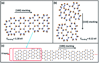
Then we stacked two structural models of (ZnTe)34 MSCs along [110] and [100] directions to simulate the growth of wurtzite ZnTe NPLs and calculated the formation energy of the resulting (ZnTe)68 MSCs (Fig. 7a and b). The binding energy was calculated as Ebinding = E68 − 2E34, where E68 and E34 are the total binding energy of (ZnTe)68 nanoclusters and the energy of (ZnTe)34 nanoclusters, respectively. The binding energy of [110] stacking and [100] stacking is −0.12 eV and −1.18 eV, respectively. For [100] stacking, the rhombic ring of one (ZnTe)34 nanocluster is opened and bonded to another (ZnTe)34 cluster, which leads to two new hexagonal rings and enhances the stability of (ZnTe)68 clusters. The calculation results show that [100] stacking is a thermodynamically spontaneous process and has more energy preferable than that of [110] stacking. Thus, we can speculate that (ZnTe)68 nanoclusters will continue to attach orientally along the [100] direction, which leads to the formation of a zigzag lateral structure (Fig. 7c) with a larger size along the [100] direction. In addition, the thickness of the zigzag lateral structure is determined to be ∼1.4 nm from the eight layers of (ZnTe)68 clusters, which is close to the experimental estimation of 1.5 nm. In summary, experimental results and DFT calculations reveal oriented attachment growth of ZnTe MSC-398 along [100] and [002] directions to form wurtzite ZnTe NPLs.
Conclusions
In conclusion, oriented attachment growth of wurtzite ZnTe nanoplatelets from metastable magic-size nanoclusters was reported. Wurtzite ZnTe NPLs were prepared using polytelluride species as the tellurium precursor reduced by Superhydrides from TBP-Te. This growth process involved a transition from self-assembled ZnTe MSC-323 to ZnTe MSC-398 and then oriented attachment growth of ZnTe MSC-398 along [100] and [002] directions. The availability of ZnTe NPLs opens the gate for extending their properties of multiple-quantum well structures to a variety of potential applications in optoelectronics, sensors and detectors.Author contributions
G. J. and C. L. conceived the project, designed the experiments and supervised the research. F. W. conducted synthesis, materials characterization and analysis. M. Z. performed the DFT simulations. C. W., S. J., H. Y., S. W., X. Y., L. Z. and M. A. B. assisted with the data analysis. F. W., M. Z., C. L. and G. J. wrote the manuscript. All the authors discussed the data, mechanisms, and commented on the manuscript.Conflicts of interest
There are no conflicts to declare.Acknowledgements
Fei Wang acknowledges the China Scholarship Council (CSC). Minyi Zhang thanks the National Natural Science Foundation of China (No. 21703246). This work was supported by the Australian Research Council Discovery Early Career Researcher Award (ARC DECRA) (Project ID: DE160100589), the Strategic Priority Research Program of the Chinese Academy of Sciences (Grant No. XDB20000000) the Hundred Talents Program of the Chinese Academy of Sciences, and the Special Program for Applied Research on Super Computation of the NSFC Guangdong Joint Fund (the second phase). The authors acknowledge the facilities, and the scientific and technical assistance of the Microscopy Australia at the Centre for Microscopy, Characterization & Analysis (CMCA), University of Western Australia.Notes and references
- J. S. Son, X. D. Wen, J. Joo, J. Chae, S. I. Baek, K. Park, J. H. Kim, K. An, J. H. Yu, S. G. Kwon, S. H. Choi, Z. Wang, Y. W. Kim, Y. Kuk, R. Hoffmann and T. Hyeon, Angew. Chem., Int. Ed., 2009, 48, 6861–6864 CrossRef CAS PubMed.
- S. Ithurria and B. Dubertret, J. Am. Chem. Soc., 2008, 130, 16504–16505 CrossRef CAS PubMed.
- Y. Chen, D. Chen, Z. Li and X. Peng, J. Am. Chem. Soc., 2017, 139, 10009–10019 CrossRef CAS.
- Y. Zhou and W. E. Buhro, J. Am. Chem. Soc., 2017, 139, 12887–12890 CrossRef CAS.
- S. Ithurria, M. D. Tessier, B. Mahler, R. P. S. M. Lobo, B. Dubertret and A. L. Efros, Nat. Mater., 2011, 10, 936–941 CrossRef CAS PubMed.
- C. Bouet, B. Mahler, B. Nadal, B. Abecassis, M. D. Tessier, S. Ithurria, X. Z. Xu and B. Dubertret, Chem. Mater., 2013, 25, 639–645 CrossRef CAS.
- S. Christodoulou, J. I. Climente, J. Planelles, R. Brescia, M. Prato, B. Martin-Garcia, A. H. Khan and I. Moreels, Nano Lett., 2018, 18, 6248–6254 CrossRef CAS.
- E. Lhuillier, S. Pedetti, S. Ithurria, B. Nadal, H. Heuclin and B. Dubertret, Acc. Chem. Res., 2015, 48, 22–30 CrossRef CAS PubMed.
- Z. Li and X. Peng, J. Am. Chem. Soc., 2011, 133, 6578–6586 CrossRef CAS PubMed.
- Z. Li, H. Y. Qin, D. Guzun, M. Benamara, G. Salamo and X. G. Peng, Nano Res., 2012, 5, 337–351 CrossRef CAS.
- S. Jana, P. Davidson and B. Abecassis, Angew. Chem., Int. Ed., 2016, 55, 9371–9374 CrossRef CAS PubMed.
- Y. Y. Liu, B. W. Zhang, H. S. Fan, N. Rowell, M. Willis, X. T. Zheng, R. C. Che, S. Han and K. Yu, Chem. Mater., 2018, 30, 1575–1584 CrossRef CAS.
- Y. Wang, Y. Zhang, F. Wang, D. E. Giblin, J. Hoy, H. W. Rohrs, R. A. Loomis and W. E. Buhro, Chem. Mater., 2014, 26, 2233–2243 CrossRef CAS PubMed.
- Y. Wang, Y. Zhou, Y. Zhang and W. E. Buhro, Inorg. Chem., 2015, 54, 1165–1177 CrossRef CAS PubMed.
- S. Sarkar, S. Acharya, A. Chakraborty and N. Pradhan, J. Phys. Chem. Lett., 2013, 4, 3292–3297 CrossRef CAS.
- D. Chen, H. Zhang, Y. Li, Y. Pang, Z. Yin, H. Sun, L. C. Zhang, S. Wang, M. Saunders and E. Barker, Adv. Mater., 2018, 30, 1803351 CrossRef PubMed.
- G. Jia, A. Sitt, G. B. Hitin, I. Hadar, Y. Bekenstein, Y. Amit, I. Popov and U. Banin, Nat. Mater., 2014, 13, 301–307 CrossRef CAS PubMed.
- J. Su, T. Minegishi, Y. Kageshima, H. Kobayashi, T. Hisatomi, T. Higashi, M. Katayama and K. Domen, J. Phys. Chem. Lett., 2017, 8, 5712–5717 CrossRef CAS PubMed.
- G. Jia and U. Banin, J. Am. Chem. Soc., 2014, 136, 11121–11127 CrossRef CAS PubMed.
- G. Jia, Y. Pang, J. Ning, U. Banin and B. Ji, Adv. Mater., 2019, 31, 1900781 CrossRef PubMed.
- Y. L. Cao, Z. T. Liu, L. M. Chen, Y. B. Tang, L. B. Luo, J. S. Jie, W. J. Zhang, S. T. Lee and C. S. Lee, Opt. Express, 2011, 19, 6100–6108 CrossRef CAS PubMed.
- K. S. Lee, G. Oh and E. K. Kim, Sol. Energy, 2018, 164, 262–266 CrossRef CAS.
- T. Loffler, T. Hahn, M. Thomson, F. Jacob and H. Roskos, Opt. Express, 2005, 13, 5353–5362 CrossRef CAS PubMed.
- J. Zhang, S. Jin, H. C. Fry, S. Peng, E. Shevchenko, G. P. Wiederrecht and T. Rajh, J. Am. Chem. Soc., 2011, 133, 15324–15327 CrossRef CAS PubMed.
- J. Zhang, C. Rowland, Y. Liu, H. Xiong, S. Kwon, E. Shevchenko, R. D. Schaller, V. B. Prakapenka, S. Tkachev and T. Rajh, J. Am. Chem. Soc., 2015, 137, 742–749 CrossRef CAS PubMed.
- J. Joo, J. S. Son, S. G. Kwon, J. H. Yu and T. Hyeon, J. Am. Chem. Soc., 2006, 128, 5632–5633 CrossRef CAS PubMed.
- S. H. Lee, Y. J. Kim and J. Park, Chem. Mater., 2007, 19, 4670–4675 CrossRef CAS.
- D. Hu, P. Zhang, P. Gong, S. Lian, Y. Lu, D. Gao and L. Cai, Nanoscale, 2011, 3, 4724–4732 RSC.
- H. Sun, F. Wang and W. E. Buhro, ACS Nano, 2018, 12, 12393–12400 CrossRef CAS PubMed.
- S. Liu, Q. Yu, C. Zhang, M. Zhang, N. Rowell, H. Fan, W. Huang, K. Yu and B. Liang, J. Phys. Chem. Lett., 2020, 11, 75–82 CrossRef CAS PubMed.
- L. Li, J. Zhang, M. Zhang, N. Rowell, C. Zhang, S. Wang, J. Lu, H. Fan, W. Huang, X. Chen and K. Yu, Angew. Chem., Int. Ed. DOI:10.1002/ange.202001608 ..
- Y. Liu, M. Willis, N. Rowell, W. Luo, H. Fan, S. Han and K. Yu, J. Phys. Chem. Lett., 2018, 9, 6356–6363 CrossRef PubMed.
- X. Ji, D. Copenhaver, C. Sichmeller and X. Peng, J. Am. Chem. Soc., 2008, 130, 5726–5735 CrossRef CAS.
- H. Park, H. Chung and W. Kim, Mater. Lett., 2013, 99, 172–175 CrossRef CAS.
- L. G. Gutsev, B. R. Ramachandran and G. L. Gutsev, J. Phys. Chem. C, 2018, 122, 3168–3175 CrossRef CAS.
- Y. Zhou, R. Jiang, Y. Wang, H. W. Rohrs, N. P. Rath and W. E. Buhro, Inorg. Chem., 2019, 58, 1815–1825 CrossRef CAS PubMed.
Footnote |
| † Electronic supplementary information (ESI) available. See DOI: 10.1039/d0na00409j |
| This journal is © The Royal Society of Chemistry 2020 |

