
High-quality epitaxial wurtzite structured InAs nanosheets grown in MBE
Qiang
Sun
 a,
Han
Gao
a,
Xutao
Zhang
bc,
Xiaomei
Yao
abc,
Shengduo
Xu
a,
Kun
Zheng
d,
Pingping
Chen
b,
Wei
Lu
be and
Jin
Zou
*af
a,
Han
Gao
a,
Xutao
Zhang
bc,
Xiaomei
Yao
abc,
Shengduo
Xu
a,
Kun
Zheng
d,
Pingping
Chen
b,
Wei
Lu
be and
Jin
Zou
*af
aMaterials Engineering, The University of Queensland, St Lucia, Queensland 4072, Australia
bState Key Laboratory for Infrared Physics, Shanghai Institute of Technical Physics, Chinese Academy of Sciences, 500 Yutian Road, Shanghai 200083, China
cUniversity of Chinese Academy of Sciences, No.19A Yuquan Road, Beijing 100049, China
dInstitute of Microstructure and Properties of Advanced Materials, Beijing University of Technology, Beijing 100124, China
eSchool of Physical Science and Technology, ShanghaiTech University, Shanghai 201210, China
fCentre for Microscopy and Microanalysis, The University of Queensland, St Lucia, Queensland 4072, Australia. E-mail: j.zou@uq.edu.au
First published on 14th November 2019
Abstract
In this study, we have grown epitaxial wurtzite structured InAs nanosheets using Au catalysts on a GaAs{111}B substrate by molecular beam epitaxy. Through detailed electron microscopy characterization studies on grown nanosheets, it was found that these wurtzite structured InAs nanosheets grew epitaxially on the GaAs{111}B substrate, with {000![[1 with combining macron]](https://www.rsc.org/images/entities/char_0031_0304.gif) } catalyst/nanosheet interfaces and extensive {11
} catalyst/nanosheet interfaces and extensive {11![[2 with combining macron]](https://www.rsc.org/images/entities/char_0032_0304.gif) 0} surfaces. It was anticipated that the epitaxially grown InAs nanosheet can be triggered by a high supersaturation in catalysts, leading to an inclined growth leaving the substrate surface, and driven by the small lattice mismatch between the nanosheets and the substrate, with the orientation relationship of (000)InAs//(11)GaAs. This study provides insights into achieving epitaxial free-standing III–V nanosheet growth.
0} surfaces. It was anticipated that the epitaxially grown InAs nanosheet can be triggered by a high supersaturation in catalysts, leading to an inclined growth leaving the substrate surface, and driven by the small lattice mismatch between the nanosheets and the substrate, with the orientation relationship of (000)InAs//(11)GaAs. This study provides insights into achieving epitaxial free-standing III–V nanosheet growth.
Introduction
Low-dimensional III–V nanostructures, such as nanowires and nanosheets, due to their superior electronic and optoelectronic properties, are promising materials for applications such as sprintronics, logic, sensing and detecting.1–9 In recent years, various free-standing low-dimensional nanosheets have been successfully fabricated using different methods.10–13 Currently, despite selected area growth on pre-patterned substrates via the vapor–solid (VS) mechanism,13 there are two common approaches using metallic nanocatalysts to induce free-standing nanosheet growth. One approach is through two-stage growth, by manipulating the growth parameters, such as tuning the V/III ratio and source species during the III–V nanowire growth, for example, Au-catalysed InP nanoflag growth from InP nanowires,10 Ag-catalysed InSb nanosheet growth from InAs nanowires,11 Au-catalysed InSb nanosheet growth from InAs nanowires,12 and Au-catalysed InAs nanosheet growth from InAs nanowires.14 On the other hand, inducing free-standing nanosheets can be realized by the direct epitaxial growth on substrates using metal nanocatalysts, such as Ag-catalysed InAs nanosheets on various substrates (Si, MgO, GaAs, etc.)15 and Au-catalysed InAs nanoplates on a GaAs{001} substrate.16 For low-dimensional nanosheets to be practically useful, the direct epitaxial growth of III–V nanosheets, due to their better controllability and the potential of direct integration with the semiconductor wafers, which can lead to compatibility with the current semiconductor industry, is highly desirable. However, the conventional catalyst-induced method and pre-patterned method are more likely to induce one-dimensional III–V nanowire growth, along 〈〉/〈000〉 directions for the zinc blende/wurtzite structures.17–24 Therefore, it still remains a challenge to achieve the epitaxial growth of novel free-standing III–V nanostructures induced by metal catalysts. On the other hand, the growth mechanism of the epitaxial growth of III–V nanosheets via the metal-catalysed method is not fully understood, and so exploring the epitaxial growth of free-standing InAs nansheets and investigating their growth mechanism are highly desirable.
In this study, we demonstrated the epitaxial growth of free-standing wurtzite structured InAs nanosheets induced by Au catalysts on a GaAs{111}B substrate in MBE. Through detailed structural and chemical characterization using advanced electron microscopy, it has been found that, the InAs nanosheets have a wurtzite structure and adopt the nanostructure/catalyst {000} interface, and that the formation of our InAs nanosheets can be triggered by a high catalyst supersaturation, leading to an inclined nanostructure growth with respect to the substrate surface (driven by small in-plane lattice mismatch between InAs nanosheets and the GaAs{111}B substrate) with the orientation relationship of (000)InAs//(11)GaAs. The extensive surfaces of our nanosheets are determined to be {110} planes, indicating that their growth is a thermodynamically dominated process by minimising the total surface energies.
Experimental
Epitaxial InAs nanostructures were grown on a GaAs{111}B substrate in a Riber 32 MBE system using Au catalysts. The GaAs{111}B substrate surface was first degassed then thermally deoxidized to desorb surface contaminants. To order to ensure an atomically flat buffer for epitaxial InAs nanostructure growth, a thin GaAs layer was deposited on the pre-cleaned GaAs{111}B substrate. Prior to growth, a thin Au film was deposited via vacuum thermal evaporation onto the surface of the GaAs{111}B substrate in the preparation chamber and then annealed at 500 °C for 20 min in the growth chamber under an As flux rate of 3.2 × 10⁻⁶ Torr, to agglomerate the Au film into nanoparticles. In the growth chamber, the growth temperature was lowered to 310 °C and an In flux was introduced to initiate the growth, leading to a V/III ratio of ∼8. The growth was terminated by shutting off the indium supply in the As atmosphere. Then the samples were cooled to room temperature slowly in an As-rich atmosphere.The morphological characteristics of Au-catalysed InAs nanosheets and nanowires were investigated using scanning electron microscopy (JEOL 7800F, operated at an 10 kV) and the structural and chemical characteristics of InAs nanostructures were investigated using transmission electron microscopy (FEI Tecnai F20 TEM, equipped with energy disperse spectroscopy (EDS) detector for compositional analysis, operated at 200 kV). For TEM characterization, individual InAs nanostructures were dispersed onto a holey carbon film supported by Cu grids.
Results and discussion
Fig. 1 shows the SEM images of Au-catalysed InAs nanostructures epitaxially grown on the GaAs{111}B substrate. Fig. 1a is a typical side-view SEM image, in which vertically grown nanowires can be seen. In addition, some inclined nanosheets can also be seen, as marked by arrows. Fig. 1b shows the composite top-view SEM images of grown nanostructures, in which inclined nanosheets, grown in different directions, can be seen on the GaAs{111}B substrate simultaneously with those vertical nanowires. Fig. 1c is a SEM image of the GaAs{111}B substrate and shows the cleaved edge, from which crystallographic information of the substrate can be identified, marked as 〈112〉 directions (red arrows) and 〈110〉 directions (green arrows). Thus, the projections of the growth direction of the nanosheets on the GaAs{111}B substrate surface can be determined to be along the 〈11〉 directions, as indicated by the red dashed lines, indicating that our nanosheets can have a fixed epitaxial relationship with the GaAs substrate. Additionally, by tilting the incident electron beam parallel to the surfaces of the nanosheets, the average thickness of our nanosheets can be determined to be ∼30 nm (refer to the inset of Fig. 1b), indicating their ultra-thin nature. The inset of Fig. 1b also shows that a catalyst at the tip of the nanosheet, suggesting that our nanosheets are induced by Au catalysts.
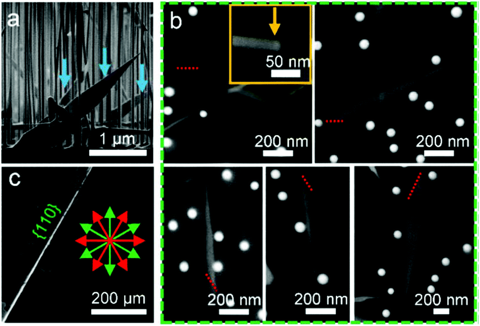 | ||
| Fig. 1 SEM investigations of Au-catalysed nanostructures. (a) Side-view SEM image of nanostructures with nanosheets indicated by arrows. (b) Composite top-view SEM images of nanostructures, in which red dashed lines indicate the connection between the nanosheets and the GaAs substrate. The inset of (b) showing the tilted-view SEM image of the top region of a typical nanosheet, where the catalyst is indicated by arrows. (c) Low-mag SEM image of the GaAs{111}B substrate showing the cleaved edge, with red arrows and green arrows representing the 〈112〉 and 〈110〉 directions that are on the {111}B surface, respectively. | ||
To understand the structural and chemical characteristics of these epitaxial nanosheets, detailed TEM characterization was performed. Fig. 2a shows a bright-field (BF) TEM image of a typical nanosheet, which is electron transparent and shows its ultra-thin nature. Fig. 2b, e, f and g show the high-resolution TEM (HRTEM) images of marked regions in Fig. 2a, respectively taken from the nanosheet/catalyst interface, the left sidewall, the right sidewall, and the bottom of the nanosheet. Fig. 2c and the insets of Fig. 2e, f, and g are their corresponding selected area electron diffraction (SAED) patterns, respectively. All these HRTEM images and SAED patterns are taken along the [110] zone-axis of the wurtzite structured nanosheets, and these TEM results indicate that grown nanosheets have (1) {000} nanosheet/catalyst interfaces that have the lowest interfacial energy in wurtzite structured III–V nanomaterials,25 and (2) extensive {110} surfaces that have low surface energy in the wurtzite structured III–V nanostructures.10,26 To determine the compositions of the catalyst and the nanostructure, EDS analysis were performed. Fig. 2d shows the EDS results obtained from the catalyst and its underlying nanosheet, in which the catalyst contains Au and In, and the nanosheets are indeed InAs (Cu signal coming from the Cu grids for TEM analysis). Based on our quantitative EDS analyses on the compositions of catalysts from several nanosheets, the In concentration in the catalysts ranges from 35 at% to 39 at%. Since Fig. 2c was taken from the catalyst/nanosheet interface, two sets of overlapped SAED patterns are seen. Using the diffraction spots of InAs as a reference (lattice parameters of wurtzite structured InAs are a = 0.4284 nm and c = 0.6996 nm),27 the lattice spacing of diffraction spots of catalysts can be determined. Based on our detailed diffraction analysis, the crystal structure of the nanosheet catalyst can be determined as the hexagonal structured Au–In Ψ phase with lattice parameters of a = 0.4538 nm and c = 0.5645 nm,28 and with a theoretical composition of 38 at% In and 62 at% Au, which is in excellent agreement with our quantitative EDS analysis on the catalysts of nanosheets.
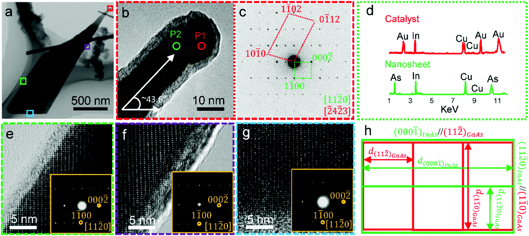 | ||
| Fig. 2 TEM investigations on a typical Au-catalysed InAs nanosheet. (a) BF TEM image of a typical nanosheet. (b) HRTEM image taken at the nanosheet/catalyst interface with the corresponding superimposed SAED pattern shown in (c). (d) EDS spectra of the catalyst and its underlying nanosheet. (e–g) HRTEM images taken from marked regions of the nanosheet (a) with insets being corresponding SAED patterns, viewed along the [110] zone-axis, respectively. (h) Schematic diagram showing the near coherent interface between (100) of the InAs nanosheets and () of the underlying GaAs substrate. | ||
To understand the formation of the nanosheet, we note that the nanosheet's top contains a section of nanowire that connects with the Au catalyst (as shown in Fig. 2b), where the diameter of the nanowire section is a constant, indicating no noticeable lateral growth at the front of the nanosheet. By examining the nanowire sections of more than a dozen nanosheets, it was found that, the angle between the [000] direction and the growth direction remains as ∼44° constantly, indicating that the growth direction of the nanowire section (as well as the nanosheet) is along the [10] direction (marked in Fig. 2b, and the theoretical angle between [000] and [10] directions is 43.6°). Additionally, due to the fact that the size of the nanosheets is much larger than that of the nanowire section, the formation of our nanosheets must be a combination of catalyst-induced axial growth along the [10] direction and the lateral growth leading to extensive {110} surfaces. It is of interest to note that a pair of parallel sidewalls can be observed. By correlating the sidewalls in the HRTEM image shown in Fig. 2e, f to their corresponding SAED patterns (as insets), a pair of {10![[3 with combining macron]](https://www.rsc.org/images/entities/char_0033_0304.gif) } side-walls can be determined, which have been often observed in close-packed hexagonal materials.29–31 In addition, a corrugated sidewall can be found close to the catalyst-induced growth front, distinguished as the upper sidewall of the grown nanosheet (see Fig. 2a), which can consist of numerous steps and result from the inclined growth, generating steps in the lateral growth. Additionally, the bottom edge of the grown nanosheet that is connected with the GaAs substrate (refer to the dashed lines shown in Fig. 1b) can be determined as the (100) plane, since the InAs (100) plane is parallel to the GaAs substrate surface and since (100)⊥(000) for InAs nanosheets, the (000) nanosheet/catalyst interfaces must be perpendicular to the substrate surface at the nucleation stage of the nanosheets (in fact, it should be the nanowire section at the initial growth of the nanosheets). To fundamentally understand the formation of the epitaxial InAs nanosheets on the lattice-mismatched GaAs substrate, the following facts should be noted: (1) The (000) planes of InAs nanosheets are parallel to the (11) planes that are perpendicular to the GaAs substrate surface, indicating an orientation relationship of (000)InAs//(11)GaAs; (2) (100) planes of InAs nanosheets are epitaxially connected with the GaAs {} substrate surface, indicating a crystallographic relationship of (100)InAs//()GaAs. From the view-point of crystallography, since the (110)InAs surface is perpendicular to the (100)InAs planes (bottoms of the InAs nanosheet), and the (11)GaAs plane is perpendicular to the (10)GaAs planes on the ()GaAs substrate surface, the (110)InAs planes must be parallel to the (10)GaAs planes, indicating the orientation relationship of (110)InAs//(10)GaAs. Due to the thin sheet nature of our nanosheets with a large surface/thickness ratio, the lattice mismatch between (000)InAs and (11)GaAs should be the key factor for the formation of the observed epitaxial growth of InAs nanosheets on the GaAs{111}B substrate. Based on our careful crystallographic analysis, the lattice spacings between 3d{11}GaAs and d{000}InAs have a surprisingly small lattice mismatch of 〈0.1%, leading to a near perfect lattice-matched orientation relationship of (000)InAs//(11)GaAs. Besides, the lattice mismatch between d{10}GaAs and 2d{110}InAs is ∼6.5%. In this regard, we anticipate that the epitaxial growth of our InAs nanosheets is driven by the small lattice mismatch between the InAs nanosheets and the GaAs substrate, as schematically illustrated in Fig. 2h, with the orientation relationships of (000)InAs//(11)GaAs and (110)InAs//(10)GaAs. In addition, we note that the nucleation of the nanosheets is in the form of nanowire nucleation, and can be similar to the planar nanowire growth,32–36 which has the key features of (1) epitaxial relationship with the substrate (crawling on the substrate along specific crystallographic directions), and (2) low-energy nanostructure/catalyst interfaces that are not parallel to the substrate surface. It is well documented that the Au catalyst can move horizontally at the initial nucleation stage of heteroepitaxial III–V nanostructure growth, driven by maintaining low interfacial energy between the Au catalyst and substrate surface.37 Therefore, due to the fact that the Au/InAs interfacial energy is higher than that of Au/GaAs interfacial energy,34,38 the Au catalysts preferentially move horizontally on the GaAs substrate to maintain their contact with the GaAs surface. Simultaneously, InAs may nucleate at the sides of the Au catalysts rather than the Au/GaAs interfaces, leading to the growth of planar nanowires.
} side-walls can be determined, which have been often observed in close-packed hexagonal materials.29–31 In addition, a corrugated sidewall can be found close to the catalyst-induced growth front, distinguished as the upper sidewall of the grown nanosheet (see Fig. 2a), which can consist of numerous steps and result from the inclined growth, generating steps in the lateral growth. Additionally, the bottom edge of the grown nanosheet that is connected with the GaAs substrate (refer to the dashed lines shown in Fig. 1b) can be determined as the (100) plane, since the InAs (100) plane is parallel to the GaAs substrate surface and since (100)⊥(000) for InAs nanosheets, the (000) nanosheet/catalyst interfaces must be perpendicular to the substrate surface at the nucleation stage of the nanosheets (in fact, it should be the nanowire section at the initial growth of the nanosheets). To fundamentally understand the formation of the epitaxial InAs nanosheets on the lattice-mismatched GaAs substrate, the following facts should be noted: (1) The (000) planes of InAs nanosheets are parallel to the (11) planes that are perpendicular to the GaAs substrate surface, indicating an orientation relationship of (000)InAs//(11)GaAs; (2) (100) planes of InAs nanosheets are epitaxially connected with the GaAs {} substrate surface, indicating a crystallographic relationship of (100)InAs//()GaAs. From the view-point of crystallography, since the (110)InAs surface is perpendicular to the (100)InAs planes (bottoms of the InAs nanosheet), and the (11)GaAs plane is perpendicular to the (10)GaAs planes on the ()GaAs substrate surface, the (110)InAs planes must be parallel to the (10)GaAs planes, indicating the orientation relationship of (110)InAs//(10)GaAs. Due to the thin sheet nature of our nanosheets with a large surface/thickness ratio, the lattice mismatch between (000)InAs and (11)GaAs should be the key factor for the formation of the observed epitaxial growth of InAs nanosheets on the GaAs{111}B substrate. Based on our careful crystallographic analysis, the lattice spacings between 3d{11}GaAs and d{000}InAs have a surprisingly small lattice mismatch of 〈0.1%, leading to a near perfect lattice-matched orientation relationship of (000)InAs//(11)GaAs. Besides, the lattice mismatch between d{10}GaAs and 2d{110}InAs is ∼6.5%. In this regard, we anticipate that the epitaxial growth of our InAs nanosheets is driven by the small lattice mismatch between the InAs nanosheets and the GaAs substrate, as schematically illustrated in Fig. 2h, with the orientation relationships of (000)InAs//(11)GaAs and (110)InAs//(10)GaAs. In addition, we note that the nucleation of the nanosheets is in the form of nanowire nucleation, and can be similar to the planar nanowire growth,32–36 which has the key features of (1) epitaxial relationship with the substrate (crawling on the substrate along specific crystallographic directions), and (2) low-energy nanostructure/catalyst interfaces that are not parallel to the substrate surface. It is well documented that the Au catalyst can move horizontally at the initial nucleation stage of heteroepitaxial III–V nanostructure growth, driven by maintaining low interfacial energy between the Au catalyst and substrate surface.37 Therefore, due to the fact that the Au/InAs interfacial energy is higher than that of Au/GaAs interfacial energy,34,38 the Au catalysts preferentially move horizontally on the GaAs substrate to maintain their contact with the GaAs surface. Simultaneously, InAs may nucleate at the sides of the Au catalysts rather than the Au/GaAs interfaces, leading to the growth of planar nanowires.
Since the majority of grown InAs nanostructures are vertically grown InAs nanowires, induced by Au catalysts, and vertical InAs nanowires grown on the GaAs{111}B substrate generally adopt {}/{000} nanowire/catalyst interfaces, which are same as the nanosheet/catalyst interfaces, it is necessary to compare the difference of the catalysts and their interfaces between the inclined nanosheets and vertical nanowires. In this regard, detailed TEM investigations were performed on these InAs nanowires. Fig. 3a shows the BF TEM image of a typical vertical nanowire. Fig. 3b is the HRTEM image taken from the top region of the nanowire, showing the sharp {000} interface, and its inset shows the SAED pattern taken from the nanowire, indicating that the nanowire has the [000] growth direction of the wurtzite structure. This observation was confirmed by our extensive TEM investigations on over one dozen of nanowires, with the average size of catalysts in nanowires being ∼10 nm, which was smaller than that of the catalysts in the nanosheets (∼17 nm). To investigate the composition of the catalysts and their underlying nanowires, EDS analysis was performed on these nanowires and their catalysts, Fig. 3c, and the EDS results show that the catalysts are Au-In alloy and the nanowires are InAs. Our quantitative EDS analysis on more than one dozen of nanowires indicates that the In concentrations of the catalysts range from 20 to 23 at%. It is interesting to note that the catalysts of nanosheets are larger than those of nanowires while having a higher In concentration. However, our previous studies39 found In atoms prefer to penetrate into smaller catalysts, leading to a higher In concentration. To clarify this contradiction, we note that the In incorporation into the Au catalysts can be influenced by the Gibbs-Thomson effect,40 where the Laplacian pressure can be significantly increased as the catalyst size shrinks, making the smaller catalysts desorb more group-III adatoms than their larger counterparts in nanosheets. On the other hand, due to the small energetic difference between the zinc blende and wurtzite structured stacking sequences along the normal of {111}/{0001} dense planes,41 defects can be easily found in wurtzite structured InAs nanostructures when observing along the [110] zone-axis. It is of interest to note that, our nanosheets have a high crystal quality (refer to the HRTEM images shown in Fig. 2d, e and f), which can result from the relatively high In supersaturation in nanosheet catalysts, enhancing the nucleation of the wurtzite structure.42
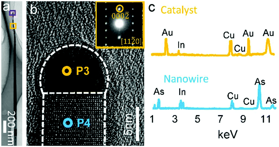 | ||
| Fig. 3 TEM investigations on Au-catalysed vertical InAs nanowires. (a) BF TEM image of a typical nanowire. (b) HRTEM image taken at the top region of the nanowire, showing the {000} nanowire/catalyst interface, inset showing the [110] zone-axis SAED pattern taken from the top region of the nanowire, indicating the [000] growth direction. (c) EDS spectra of the catalyst and its underlying nanowire respectively. | ||
To comprehensively understand why nanosheets are induced with {000} nanostructure/catalyst interfaces by Au catalysts, while having a non-〈000〉 growth direction, and exhibiting a free-standing morphology on the substrate, we first note that, both catalysts of nanowires and nanosheets are hemisphere-shaped, indicating that their growth is dominated by the VLS mechanism.43 In this regard, supersaturation, determined by the In concentration in the Au–In alloy particles due to its crucial role in the nanostructure growth,44 should be carefully investigated. To understand the influence of catalyst supersaturation in the growth, the following two facts should be considered: (1) The nanostructure/catalyst interfaces are {000} for nanosheets and nanowires. (2) The supersaturation in the nanosheet catalysts is higher than that in the catalysts of nanowires. Based on these facts, we note that, according to the kinetic model of nanostructure growth with {000} interfaces,45 a higher supersaturation in the catalysts favours the inclined growth. Therefore, once the catalysts reach a relatively high catalyst supersaturation in the nanostructure nucleation stage, the inclined growth can be triggered, leading to the out-of-plane growth (described as “taking off” in planar nanowire growth36) and leaving the substrate surface.
Based on our comprehensive experimental characterization and discussion outlined above, Fig. 4 illustrates the proposed model of the growth of Au-catalysed nanosheets. Prior the growth, the deposited Au film was annealed and agglomerated into Au nanoparticles on the substrate surfaces, due to the Ostwald ripening effect.46 After introducing the In source into the growth chamber, Au nanoparticles absorb In adatoms and form Au catalysts. Fig. 4a illustrates the nucleation of a nanosheet, viewed along the [10] direction of the GaAs substrate, showing that, once the growth was triggered, InAs crystallizes with catalysts by adopting the (000) nanosheet/catalyst interface, which is perpendicular to the substrate surface. Fig. 4b shows the catalyst-induced axial growth of the nanosheet and its lateral growth, leading to the formation of the nanosheet. Fig. 4c and d show the schematic view of the nanosheet in Fig. 4b, viewed along the [111] and [10] directions of the GaAs substrate, respectively.
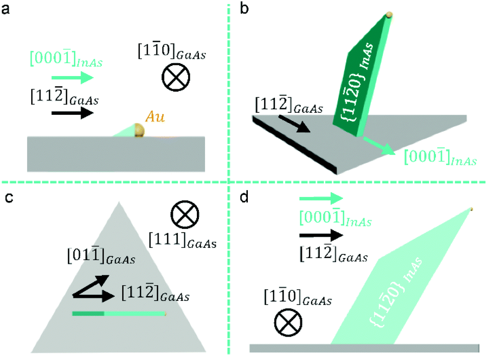 | ||
| Fig. 4 Schematic diagram showing the growth model of nanosheet growth via the VLS mechanism. (a) Nanostructure nucleation, viewed along [10] of GaAs. (b) Nanosheet growth. (c and d) Schematic views of the individual nanosheet in (b), along the [111] and [10] directions of GaAs, respectively. | ||
Conclusions
In this study, we have achieved the epitaxial growth of free-standing wurtzite structured InAs nanosheets induced by Au catalysts in MBE. Based on our detailed electron microscopy characterization on the obtained wurtzite structured nanosheets, their fundamental growth mechanism is investigated. It is found that our epitaxially grown wurtzite structured nanosheets with extensive {110} surfaces can be initialled from the planar nanowire growth on the GaAs{111}B substrate surface, triggered by a high catalyst supersaturation, which can lead to inclined nanostructure growth, and driven by the small in-plane lattice mismatch between nanosheets and the substrate, with the orientation relationship of (000)InAs//(11)GaAs. We believe our study will inspire new avenues to achieving epitaxial growth of wurtzite structured III–V nanosheets.
Conflicts of interest
There are no conflicts to declare.Acknowledgements
This research was supported by the Australian Research Council, the National Key R&D Program of China (No. 2016YFB0402401), the National Natural Science Foundation of China (No. 11634009 and 11774016) and the Key Programs of Frontier Science of the Chinese Academy of Sciences (No. QYZDJ-SSW-JSC007). The Australian Microscopy & Microanalysis Research Facility is also gratefully acknowledged for providing microscopy facilities for this study.Notes and references
- C. Thelander, T. Mårtensson, M. T. Björk, B. J. Ohlsson, M. W. Larsson, L. R. Wallenberg and L. Samuelson, Appl. Phys. Lett., 2003, 83, 2052–2054 CrossRef CAS.
- H. A. Nilsson, P. Caroff, C. Thelander, E. Lind, O. Karlström and L.-E. Wernersson, Appl. Phys. Lett., 2010, 96, 153505 CrossRef.
- F. Seker, K. Meeker, T. F. Kuech and A. B. Ellis, Chem. Rev., 2000, 100, 2505–2536 CrossRef CAS PubMed.
- L. Samuelson, C. Thelander, M. T. Bjork, M. Borgstrom, K. Deppert, K. A. Dick, A. E. Hansen, T. Martensson, N. Panev, A. I. Persson, W. Seifert, N. Skold, M. W. Larsson and L. R. Wallenberg, Physica E, 2004, 25, 313–318 CrossRef CAS.
- P. Ye, G. Wilk, B. Yang, J. Kwo, S. Chu, S. Nakahara, H.-J. Gossmann, J. Mannaerts, M. Hong and K. Ng, Appl. Phys. Lett., 2003, 83, 180–182 CrossRef CAS.
- F. Seker, K. Meeker, T. F. Kuech and A. B. Ellis, Chem. Rev., 2000, 100, 2505–2536 CrossRef CAS PubMed.
- J. D. Sau, R. M. Lutchyn, S. Tewari and S. D. Sarma, Phys. Rev. Lett., 2010, 104, 040502 CrossRef PubMed.
- J. Wang, M. S. Gudiksen, X. Duan, Y. Cui and C. M. Lieber, Science, 2001, 293, 1455 CrossRef CAS PubMed.
- H. J. Joyce, Q. Gao, H. H. Tan, C. Jagadish, Y. Kim, J. Zou, L. M. Smith, H. E. Jackson, J. M. Yarrison-Rice, P. Parkinson and M. B. Johnston, Prog. Quantum Electron., 2011, 35, 23–75 CrossRef.
- A. Kelrich, O. Sorias, Y. Calahorra, Y. Kauffmann, R. Gladstone, S. Cohen, M. Orenstein and D. Ritter, Nano Lett., 2016, 16, 2837–2844 CrossRef CAS PubMed.
- D. Pan, D. X. Fan, N. Kang, J. H. Zhi, X. Z. Yu, H. Q. Xu and J. H. Zhao, Nano Lett., 2016, 16, 834–841 CrossRef CAS PubMed.
- M. de la Mata, R. Leturcq, S. R. Plissard, C. Rolland, C. Magén, J. Arbiol and P. Caroff, Nano Lett., 2016, 16, 825–833 CrossRef CAS PubMed.
- J. Seidl, J. G. Gluschke, X. Yuan, S. Naureen, N. Shahid, H. H. Tan, C. Jagadish, A. P. Micolich and P. Caroff, Nano Lett., 2019, 19, 4666–4677 CrossRef CAS PubMed.
- Q. Sun, H. Gao, X. Yao, K. Zheng, P. Chen, W. Lu and J. Zou, Nano Res., 2019, 12, 2718–2722 CrossRef CAS.
- D. Pan, J. Y. Wang, W. Zhang, L. Zhu, X. Su, F. Fan, Y. Fu, S. Huang, D. Wei, L. Zhang, M. Sui, A. Yartsev, H. Xu and J. Zhao, Nano Lett., 2019, 19, 1632–1642 CrossRef CAS PubMed.
- M. Aagesen, E. Johnson, C. B. Sørensen, S. O. Mariager, R. Feidenhans'l, E. Spiecker, J. Nygård and P. E. Lindelof, Nat. Nanotechnol., 2007, 2, 761 CrossRef CAS PubMed.
- K. A. Dick, P. Caroff, J. Bolinsson, M. E. Messing, J. Johansson, K. Deppert, L. R. Wallenberg and L. Samuelson, Semicond. Sci. Technol., 2010, 25, 024009 CrossRef.
- K. A. Dick, C. Thelander, L. Samuelson and P. Caroff, Nano Lett., 2010, 10, 3494–3499 CrossRef CAS PubMed.
- M. Tornberg, D. Jacobsson, A. R. Persson, R. Wallenberg, K. A. Dick and S. Kodambaka, Nano Lett., 2019, 19, 3498–3504 CrossRef CAS PubMed.
- A. Li, J. Zou and X. Han, Sci. China Mater., 2016, 59, 51–91 CrossRef CAS.
- H. Gao, W. Sun, Q. Sun, H. H. Tan, C. Jagadish and J. Zou, Nano Lett., 2019, 19, 3782–3788 CrossRef CAS PubMed.
- F. Gao, L. Wen, Z. Xu, J. Han, Y. Yu, S. Zhang and G. Li, Small, 2017, 13, 1603775 CrossRef PubMed.
- J. Shen, Y. Zheng, Z. Xu, Y. Yu, F. Gao, S. Zhang, Y. Gan and G. Li, Nanoscale, 2018, 10, 21951–21959 RSC.
- Z. Xu, Y. Yu, J. Han, L. Wen, F. Gao, S. Zhang and G. Li, Nanoscale, 2017, 9, 16864–16870 RSC.
- C. E. Dreyer, A. Janotti and C. G. Van de Walle, Phys. Rev. B, 2014, 89, 081305 CrossRef.
- N. Sibirev, M. Timofeeva, A. Bol'shakov, M. Nazarenko and V. DubrovskiÄ, Phys. Solid State, 2010, 52, 1531–1538 CrossRef CAS.
- M. Paladugu, J. Zou, Y.-N. Guo, X. Zhang, H. J. Joyce, Q. Gao, H. H. Tan, C. Jagadish and Y. Kim, Angew. Chem., Int. Ed., 2009, 48, 780–783 CrossRef CAS PubMed.
- S. Hiscocks and W. Hume-Rothery, Proc. R. Soc. London, Ser. A, 1964, 282, 318–330 CrossRef CAS.
- M. Niewczas, Acta Mater., 2010, 58, 5848–5857 CrossRef CAS.
- J. Wang, I. J. Beyerlein, J. P. Hirth and C. N. Tomé, Acta Mater., 2011, 59, 3990–4001 CrossRef CAS.
- J. Nie, Y. Zhu, J. Liu and X.-Y. Fang, Science, 2013, 340, 957–960 CrossRef CAS PubMed.
- Y. Zi, K. Jung, D. Zakharov and C. Yang, Nano Lett., 2013, 13, 2786–2791 CrossRef CAS PubMed.
- S. A. Fortuna, J. Wen, I. S. Chun and X. Li, Nano Lett., 2008, 8, 4421–4427 CrossRef CAS PubMed.
- X. Zhang, J. Zou, M. Paladugu, Y. Guo, Y. Wang, Y. Kim, H. J. Joyce, Q. Gao, H. H. Tan and C. Jagadish, Small, 2009, 5, 366–369 CrossRef CAS PubMed.
- W. Sun, Y. Guo, H. Xu, Q. Gao, H. H. Tan, C. Jagadish and J. Zou, Appl. Phys. Lett., 2013, 103, 223104 CrossRef.
- C. Zhang, X. Miao, P. K. Mohseni, W. Choi and X. Li, Nano Lett., 2014, 14, 6836–6841 CrossRef CAS PubMed.
- S. Breuer, M. Hilse, L. Geelhaar and H. Riechert, J. Cryst. Growth, 2011, 323, 311–314 CrossRef CAS.
- M. Paladugu, J. Zou, Y. N. Guo, G. J. Auchterlonie, H. J. Joyce, Q. Gao, H. H. Tan, C. Jagadish and Y. Kim, Small, 2007, 3, 1873–1877 CrossRef CAS PubMed.
- Z. Zhang, Z. Y. Lu, P. P. Chen, H. Y. Xu, Y. N. Guo, Z. M. Liao, S. X. Shi, W. Lu and J. Zou, Appl. Phys. Lett., 2013, 103, 073109 CrossRef.
- C. B. Maliakkal, N. Hatui, R. D. Bapat, B. A. Chalke, A. A. Rahman and A. Bhattacharya, Nano Lett., 2016, 16, 7632–7638 CrossRef CAS PubMed.
- U. Krishnamachari, M. Borgstrom, B. J. Ohlsson, N. Panev, L. Samuelson, W. Seifert, M. W. Larsson and L. R. Wallenberg, Appl. Phys. Lett., 2004, 85, 2077–2079 CrossRef CAS.
- F. Glas, J.-C. Harmand and G. Patriarche, Phys. Rev. Lett., 2007, 99, 146101 CrossRef PubMed.
- S. Kodambaka, J. Tersoff, M. Reuter and F. Ross, Science, 2007, 316, 729–732 CrossRef CAS PubMed.
- C. Zhou, K. Zheng, Z. Y. Lu, Z. Zhang, Z. M. Liao, P. P. Chen, W. Lu and J. Zou, J. Phys. Chem. C, 2015, 119, 20721–20727 CrossRef CAS.
- J. Wang, S. b. R. Plissard, M. A. Verheijen, L.-F. Feiner, A. Cavalli and E. P. Bakkers, Nano Lett., 2013, 13, 3802–3806 CrossRef CAS PubMed.
- P. W. Voorhees, J. Stat. Phys., 1985, 38, 231–252 CrossRef.
| This journal is © The Royal Society of Chemistry 2020 |