DOI:
10.1039/C9NR07541K
(Paper)
Nanoscale, 2020,
12, 277-288
Largely enhanced thermoelectric effect and pure spin current in silicene-based devices under hydrogen modification
Received
31st August 2019
, Accepted 15th November 2019
First published on 15th November 2019
Abstract
Based on the density functional theory and nonequilibrium Green's function methods, we launch a systematic study of the magnetic properties and thermoelectric effects in silicene-based devices constructed by using zigzag silicene nanoribbons (ZSiNRs). By modulating the adsorption site, it is found that the ground state of ZSiNRs varies from an antiferromagnetic state to a ferromagnetic state. Meanwhile, a spin-degenerate semiconductor evolves into a spin semiconductor. The spin and charge thermoelectric figure of merits have an almost equal value of about 60 in the narrow device, which originates from the spin-dependent conductance dips and high spin-filtering effects. Moreover, a thermally-driven pure spin current in the silicene-based devices is obtained in the absence of the gate voltage, and its magnitude is effectively enhanced as the device width increases. Our results suggest that the silicene-based devices have very good prospects for spin caloritronics.
I. Introduction
Silicene, a silicon analogue of graphene, is attracting widespread attention in the scientific community for its exotic properties.1–3 Unlike the planar structure of graphene, silicene prefers a low-buckled (LB) honeycomb structure due to a mixed sp2–sp3 hybridization.4 Similar to graphene, LB silicene exhibits semi-metal properties, and a Dirac cone is centered at the K point in the Brillouin zone. Experiments have demonstrated that silicene could grow on various metallic substrates, such as Ag,5 ZrB2,6 and Ir.7 However, the zero-energy band structure of silicene severely handicaps its applications in electronics and optoelectronics, though the first-principles calculations have predicted that a band gap of 1.55 meV is opened at the Dirac cone under the influence of spin–orbit coupling.8
Reducing the dimension of the materials can enhance their electronic and magnetic properties.9–15 Particularly, nanoribbons, one-dimensional (1D) nanomaterials, have been widely investigated owing to their potential applications in nanoscience.16–18 It has been demonstrated that the silicene nanoribbons (SiNRs) can be spontaneously ordered on Ag(001) and Ag (110) surfaces in the experiments.19,20 The structures of SiNRs are similar to those of graphene nanoribbons (GNRs). Therefore, SiNRs can also be divided into armchair silicene nanoribbons (ASiNRs) and zigzag silicene nanoribbons (ZSiNRs) according to the edge geometry structures. Their electronic and magnetic properties have been widely investigated by using first-principles calculations,21–23 and the results show that SiNRs have similar properties to GNRs.24 For example, ASiNRs can be metals or semiconductors depending on the ribbon width, and ZSiNRs are the antiferromagnetic (AFM) semiconductors. However, all ASiNRs and ZSiNRs in the ground states are nonmagnetic. To extend the applications of SiNRs in spintronics, magnetism needs to be introduced by various methods.25–30 In addition, a large magnetoresistance effect is also observed in ZSiNRs,22 and the order can reach 104. On the basis of these transport characteristics, one can design ZSiNR-based logic devices.
The thermoelectric properties of ASiNRs and ZSiNRs have also been investigated using nonequilibrium Green's function method and molecular dynamics simulations.31 The results show that these nanoribbons are very stable when the edge atoms are passivated by hydrogens, and ASiNRs exhibit much better thermoelectric effects than ZSiNRs, which are similar to the thermoelectric properties that are found in GNRs.32 Recently, the spin Seebeck effect (SSE) provides an effective way to generate a pure spin current only under the temperature difference.33 It was first detected in the ferromagnetic (FM) metal Ni81Fe19 films via the inverse spin Hall effect (ISHE).34 Soon after, the SSE was also found in the insulating ferrimagnet LaY2Fe5O12. More recently, Hong et al. have also detected a spin Seebeck signal below 300 K in a nonferromagnetic insulator SrFeO3−δ.35 In addition, as an application, the SSE can be used to probe short-range magnetic correlations and unconventional magnetic excitation in multivariate compound materials.36,37 It is well known that quantum size effects and band engineering of graphene and graphene-like nanoribbons have stimulated great interest in the spin-resolved thermoelectric effects of these low-dimensional materials.38–47 It should be noted that a spin-Seebeck diode could be achieved in ZSiNR-based heterojunctions, where some interesting transport properties, such as negative differential thermoelectric resistance (NDTR) and spin thermoelectric rectification (STR), are observed.48 In previous studies, we found that spin semiconducting properties in doped ZSiNRs, and the thermally-induced pure spin current were achieved by modulating the ribbon width.49 In addition, spin-semiconducting properties are also found in the sawtooth GNRs and SiNRs, where the charge densities of the edge bands near the Fermi level are spatially separated at different edges.50,51 Compared with the sawtooth GNRs, the sawtooth SiNRs have more stable structures due to lower formation energies.51
Hydrogenation as the most important chemical functionalization can open a band gap at the Dirac point of graphene.52 Silicene has similar electronic structures, and it is therefore natural to expect that a band gap also appears in silicene under hydrogenation. Qiu et al. performed experimentally the hydrogenation of silicene, where only one Si sublattice is fully hydrogenated.53 More recently, Zhang et al. have found that the ground state of the ZSiNRs could be changed from the antiferromagnetic (AFM) state to the FM state under hydrogen adsorption, and meanwhile the nonmagnetic semiconductor became a magnetic metal. When an electric bias is applied, a perfect spin-filtering effect and an obvious switching effect are found.28 In this paper, we present a systematic study of the magnetic properties and SSEs of silicene-based devices under hydrogen modifications. As the adsorption site changes, the ground state of ZSiNRs varies from an AFM state to a FM state. Meanwhile the wider spin-dependent band gaps are opened, leading to the huge spin and charge thermoelectric figure of merits (FOMs) of about 60 in some chemical potential regions. In the absence of the gate voltage, a nearly pure spin current appears only under the temperature difference, and its magnitude can be increased with the ribbon length.
II. Models and methods
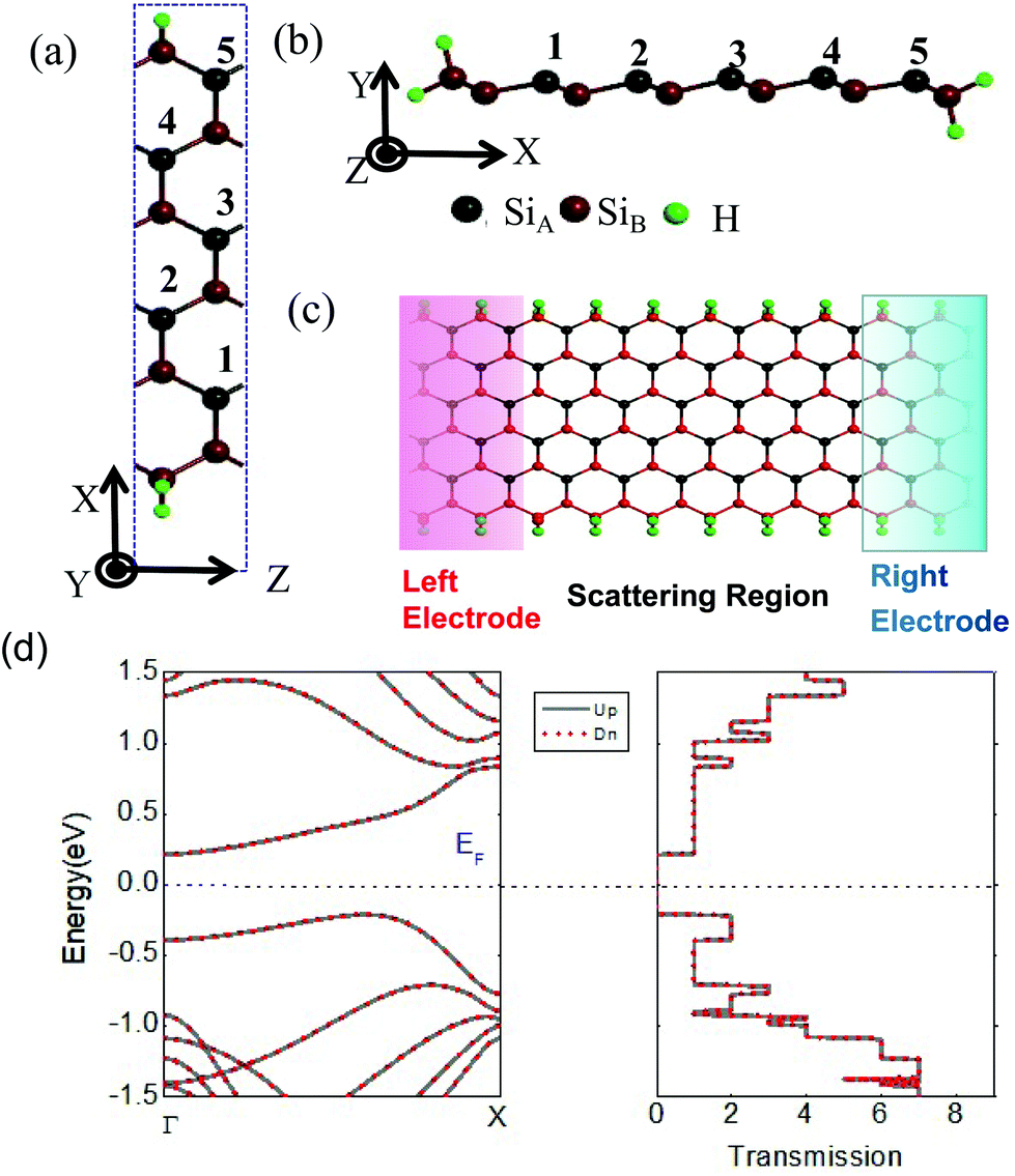
The silicene-based device is constructed by using the N-ZSiNR, which includes three regions: the left electrode, the scattering region and the right electrode. The capital N denotes the width of the ZSiNR, characterized by the number of Si atoms along the x axis. Top and side views of the 6-ZSiNR unit cell are plotted in Fig. 1(a) and (b), respectively. In order to improve the stability of devices, each Si atom in the edges of the 6-ZSiNR is terminated by two hydrogen atoms. In Fig. 1(c), as an example, we depict a silicene-based device, which is built using the 6-ZSiNR. Geometric optimization is performed by using the Vienna Ab initio Simulation Package (VASP),54,55 and the nanodcal package is used to realize the calculations for the energy band structures and transport properties.56 For these density functional calculations, the exchange correlation potential is described by the spin generalized gradient approximation (GGA) with Perdew–Burke–Ernzerhof (PBE).57 We choose a vacuum layer of larger than 15 Å thickness to avoid the interaction between periodic images along the x and y axes. Here the wave functions are expanded in a basis set of double-ξ orbitals plus one polarization orbital (DZP). The energy cutoff is 150 Ry, and the mesh grids in k-space are chosen to be 1 × 1 × 21 and 1 × 1 × 100 for the calculations of the band structure and transport properties, respectively. Within the nonequilibrium Green's function methods, one can calculate the spin-dependent current under the spin-dependent bias voltage (ΔV↑(↓)) and temperature difference (ΔT) by using the Landauer–Büttiker formula,58| | 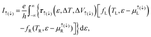 | (1) |
where e is the electronic charge and h is the Planck constant. fL(R) is the Fermi–Dirac distribution for the left (right) electrode, and μ↑(↓)L(R) = EF + (−)ΔV↑(↓)/2 and TL(R) = T + (−)ΔT/2 indicate the electrochemical potential and the temperature of the left (right) electrode, respectively. τ↑(↓) = Tr[Γ↑(↓), LGR↑(↓)Γ↑(↓), RGA↑(↓)] is the spin-up (spin-down) electronic transmission function through the two-probe device, where Γ↑(↓), L and Γ↑(↓), R are the spin-dependent electronic coupling matrixes between the scattering region and left and right electrodes, respectively, and GR(A)↑(↓) is the spin-dependent electronic retarded (advanced) Green's function of the scattering region.
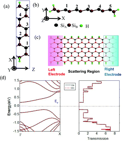 |
| | Fig. 1 (a) Top and side (b) views of the pristine 6-ZSiNR, and the edge Si atoms are terminated with two hydrogen atoms. The numbers 1, 2, 3, 4 and 5 indicate the five different adsorption positions. (c) Two-probe device based on the pristine 6-ZSiNR. (d) Spin-resolved band structure and transmission function of the pristine 6-ZSiNR. The Fermi energy EF is fixed at zero energy. | |
Under a linear response regime (ΔT → 0), we can derive the spin-dependent Seebeck coefficient S↑(↓) (defined as S↑(↓) = ΔV↑(↓)/ΔT) by letting ΔI↑(↓) = 0. After expanding the Fermi–Dirac distribution function to the first order in ΔT and ΔV↑(↓), we can obtain59,60
| |  | (2) |
where the intermediate function
Lν, ↑(↓)(
ν = 0, 1, 2) is calculated by using
with
μL =
μR =
μ and
TL =
TR =
T (in this case
fL =
fR =
f). Since the electron–phonon coupling in silicene is weak, we here ignore its contributions to the electronic and phononic transports. Thus the spin-dependent thermal conductance
κel,↑(↓) from the electron's contribution is obtained by using,
61| | 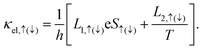 | (3) |
Similar to the computational processes for the electronic transport, the thermal conductance from the phonon's contribution can be calculated by using,39
| | 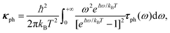 | (4) |
where
ω is the phonon frequency and
τph(
ω) denotes the phonon transmission function.
τph(
ω) can be calculated by using the Caroli formula
τph(
ω) =
Tr[
Γph, LGRphΓph, RGAph], where
Γph, L(R) are the phononic broadening functions that describe the coupling between the left (right) electrode and the scattering region, and
GR(A)ph represent the phononic retarded (advanced) Green's function of the scattering region.
62 The spin-dependent electrical conductance can be obtained by using
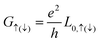
, and the spin and charge electrical conductance are defined by
GS =
G↑−
G↓ and
GC =
G↑ +
G↓,
38 respectively. By using the transport parameters defined above, the charge (spin) thermoelectric efficiency is characterized by the charge (spin) FOM
ZC(S)T =
S2CGC(S)T/(
κel, ↑ +
κel, ↓ +
κph),
38 where
SC =
S↑ +
S↓ and
SS =
S↑−
S↓ are the charge and spin Seebeck coefficients, respectively.
III. Results and discussion
In this paper, the edge Si atoms are terminated with two hydrogen atoms, and the previous research has also indicated that the dihydrogenated edges can enhance the stabilization of the AFM semiconducting ground state of ZSiNRs.63 We first consider the ZSiNRs with the ribbon width of N = 6. The top and side views of the 6-ZSiNR are depicted in Fig. 1(a) and (b), respectively, and the numbers 1, 2, 3, 4, and 5 denote the adsorption position of the single hydrogen atom. In order to explore the transport properties, we construct a two-probe system based on the 6-ZSiNR (see Fig. 1(c)). The corresponding spin-resolved band structure and spin-resolved transmission function in the ground state are presented in Fig. 1(d). The figure clearly shows that the 6-ZSiNR is a nonmagnetic semiconductor with an indirect bandgap of about 0.4 eV. The gap is also well visible in the transmission spectrum, and the spin-resolved transmission function can also be obtained by a band-counting method.64 Therefore, we observe some steps with integers in the spin-resolved transmission spectrum (see Fig. 1(d)), and these results are also in good agreement with the previous study.65
In order to extend their applications in spintronics, the spin degeneracy could be opened by introducing a single hydrogen atom adsorption in the 6-ZSiNR unit cell. Five different hydrogen adsorption sites on the 6-ZSiNR are shown in Fig. 1(b), and the 6-ZSiNR under the hydrogen atom adsorption is labelled as 6-ZSiNR1, 6-ZSiNR2, 6-ZSiNR3, 6-ZSiNR4, and 6-ZSiNR5, respectively. In the following, we first calculate the adsorption energy of the hydrogen atom on the 6-ZSiNR unit cell by using,
| | 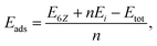 | (5) |
where
Etot is the total energy of the 6-ZSiNR after the hydrogen atom adsorption and
E6Z stands for the energy of the 6-ZSiNR in the absence of the hydrogen adsorption.
n is the number of adatoms, and
Ei represents the energy of the isolated adatoms. Since only one hydrogen atom is adsorbed on the 6-ZSiNR, we here take
n = 1. The larger positive
Eads means the stronger adsorption of the single hydrogen atom on the 6-ZSiNR, indicating that the geometry structure is more stable.
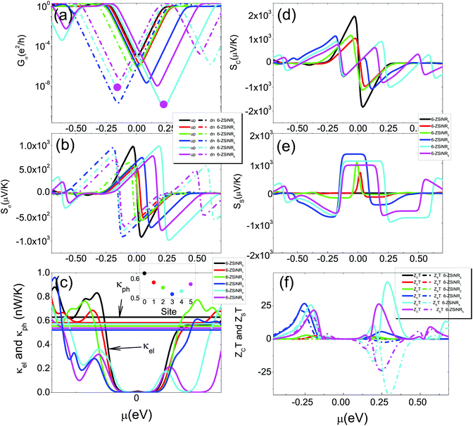
Eads at five different sites is shown in
Fig. 2(a). It is discovered that the single hydrogen atom prefers to adsorb at site 5. In addition, we also calculate the energy difference Δ
E between the FM and AFM states for the five 6-ZSiNRs under hydrogen atom adsorption, which is obtained by using,
| | | ΔE = EFM, i − EAFM, i, | (6) |
where
EFM, i(
EAFM, i) is the energy of 6-ZSiNR
i in the FM (AFM) state, and
i(= 1, 2, 3, 4, and 5) is the adsorption site.
i = 0 represents the pristine 6-ZSiNR in the absence of hydrogen adsorption. The numerical results are shown in
Fig. 2(b). For the pristine 6-ZSiNR
0, the ground state is the AFM state due to Δ
E0 > 0. As
i increases, the ground spin state is changed from the AFM state to the FM state. For example, for 6-ZSiNR
5, the energy of the FM state is about 20 meV smaller than that of the AFM state, indicating that the FM state is in its ground state. A larger energy difference between the FM and AFM states appears at site 4 (Δ
E ≈ 38 meV). The spin density distributions of these ZSiNRs in the ground state are shown in
Fig. 2(c). As per the above descriptions, the ground state of the pristine 6-ZSiNR is the AFM state with zero net spin, where the polarized spins are mainly localized at the interedge Si atoms and the spins at the two interedges are antiparallel. As the distance from the interedge increases, the spin density is rapidly suppressed. After one hydrogen atom is adsorbed, the magnetic moment of the Si atom at the adsorption site is completely suppressed. Moreover, the polarized spins mainly appear in the one side of the adsorption site (see
Fig. 2(c)), which can be well explained by Lieb's theorem.
66 It should be noted that the number difference of Si atoms in the A sites (Si
A in
Fig. 1(b)) and B sites (Si
B in
Fig. 1(b)) in the left side of the adsorption site is one, while the number difference of Si atoms in the A sites and B sites in the right side of the adsorption site is zero. Therefore, the spin densities mainly distribute in the left side of the adsorption site, and the spins in the region are arranged in a FM structure. Particularly, when the hydrogen atom is adsorbed at sites 4 and 5, a stable FM state is achieved.
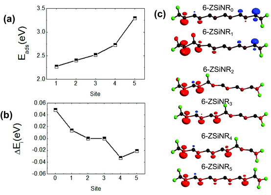 |
| | Fig. 2 (a) The adsorption energy of the 6-ZSiNR unit cell with a single hydrogen atom at five different sites. (b) The energy difference between the 6-ZSiNRi(=0, 1, 2, 3, 4, 5) in the FM and AFM states. (c) Spin densities of 6-ZSiNRi(=0, 1, 2, 3, 4, 5) in the ground states. The isosurface is 0.003 e Å−1. Red and blue surfaces represent the spin-up and spin-down components, respectively. Here 6-ZSiNR0 denotes the pristine 6-ZSiNR in the absence of hydrogen adsorption. | |
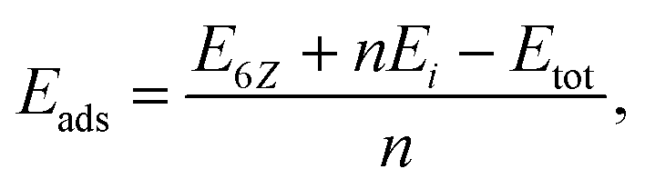
The spin-resolved band structures of 6-ZSiNRi=(1–5) in their spin ground states are presented in Fig. 3(a1–a5), and these figures clearly show that 6-ZSiNRi under hydrogen adsorption behaves like a magnetic semiconductor with a spin-resolved band gap near the Fermi level. As i changes from 1 to 5, the spin-dependent band gap is opened and enlarged. For 6-ZSiNR4 and 6-ZSiNR5, the first electronic state below the Fermi level is contributed by one narrow spin-up channel, while the first electronic state above the Fermi level is dominated by one narrow spin-down channel. With a further decrease (increase) in energy, the second electronic state below (above) the Fermi level is contributed by the spin-down (spin-up) channel. From higher energies to lower energies, these bands around the Fermi level can be called the spin-up conduction band (CB), spin-down CB, spin-up valence band (VB) and spin-down VB, respectively. In Fig. 3(c), we plot the energy positions of spin-up (spin-down) CB minimum (CBM) and VB maximum (VBM). Obviously, these bands are spin-dependent, and a spin band gap ES appears in 6-ZSiNRi=(1–5). Here ES is measured by the energy difference between the spin-up VBM and spin-down CBM, as shown in Fig. 3(d). The figure shows that all 6-ZSiNRs under hydrogen adsorption exhibit spin-semiconducting properties with a band gap of about 0.4 eV. These spectral band distributions near the Fermi level will bring interesting spin-resolved thermoelectric transport properties of the two-probe system based on 6-ZSiNRi. The corresponding spin-resolved transmission function versus E−EF is plotted in Fig. 3(b1–b5). Since the periodicity of 6-ZSiNRi is well maintained in the two-probe system, the spin-resolved transmission function can be obtained by counting the number of bands. For example, at E–EF = 0.24 eV in 6-ZSiNR5, τ↓ = 3 means that three spin-down channels are opened, and in this case the spin-down CB goes through the energy three times [see green line in Fig. 3(a5)]. These spin-dependent band gaps strongly influence the spin-dependent transport properties, and the large thermoelectric effects can be predicted.
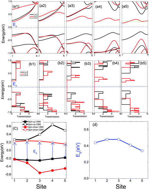 |
| | Fig. 3 (a) Spin-resolved band structures of 6-ZSiNRi(=1, 2, 3, 4, 5) in the ground states. (b) Corresponding spin-resolved transmission functions of the two-probe devices based on 6-ZSiNRi(=1, 2, 3, 4, 5). Black and red lines denote spin-up and spin-down components, respectively; from left to right, i is taken to be 1, 2, 3, 4 and 5. (c) The energy positions of the spin-up and spin-down VBM and CBM versus the adsorption site. (d) Spin gap versus the adsorption site. | |
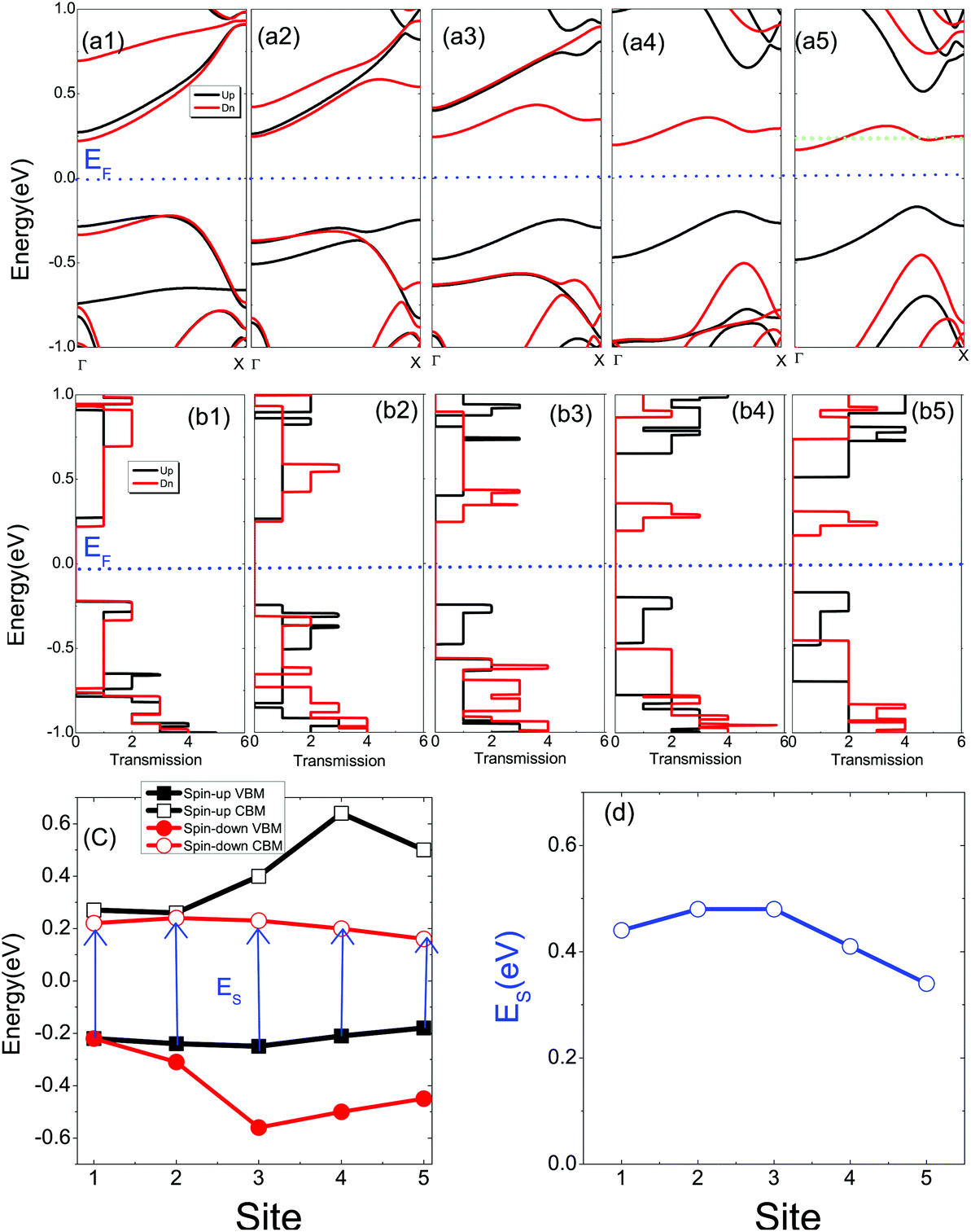
The room-temperature spin-resolved conductance G↑(↓) for 6-ZSiNRi=0, 1, 2, 3, 4, 5versus the chemical potential μ is plotted in Fig. 4(a), which can be calculated by using G↑(↓) = e2/hL0, ↑(↓). From this figure, we note that these spin-dependent band gaps result in the minimum of G↑(↓) in the middle region of these band gaps, forming the spin-resolved conductance dips. For the positive μ region, just above the Fermi level, the spin-up conductance dips are observed, while the spin-down conductance dips appear in the negative μ region, just below the Fermi level. In the low temperature region, using Sommerfeld expansion,67 one can simply write eqn (2) as
| | 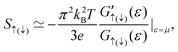 | (7) |
which clearly shows that the sign of
S↑(↓) is determined by the slope of
G↑(↓) at
μ, and its magnitude is inversely proportional to
G↑(↓) at
μ. As a result, in the vicinity of these spin-dependent conductance dips,
S↑(↓) is strongly enhanced, as shown in
Fig. 4(b). A huge positive value of
S↑(↓) appears on the left side of the spin-up (spin-down) conductance dips due to
G′
↑(↓) < 0, and a huge negative value of
S↑(↓) appears on the right side of the spin-up (spin-down) conductance dip due to
G′
↑(↓) > 0. The maximum values of |
S↑(↓)| are far larger than those reported in single-molecule heterojunctions.
68 For 6-ZSiNR
4, a huge value of |
S↑|, close to 980 μV K
−1, is achieved near the spin-up conductance dip (marked by the solid magenta dot in
Fig. 4(a)) above the Fermi level, while a huge value of |
S↓|, close to 800 μV K
−1, appears near the spin-down conductance dip below the Fermi level (marked by the solid magenta dot in
Fig. 4(a)). More interestingly, in the region close to
μ = 0,
S↑(>0) and
Sw(<0) keep the opposite sign, implying that a larger spin Seebeck coefficient than the corresponding charge Seebeck coefficient is achieved. This feature can be seen in
Fig. 4(d) (
SCversus μ) and
Fig. 4(e) (
SSversus μ). In the absence of hydrogen atom adsorption, only charge Seebeck effects can occur due to the equivalent spin channels (see black in
Fig. 4(e), here
SS = 0). When the hydrogen atom is adsorbed on the 6-ZSiNR, the spin Seebeck effect is obviously enhanced. Especially for 6-ZSiNR
3, 6-ZSiNR
4 and 6-ZSiNR
5,
SS in the transport gap near
μ = 0 remains nearly unchanged, and then a flat is observed, as shown in
Fig. 4(e). This phenomenon results mainly from a constant difference between
S↑ and
S↓ near the Fermi level. The width of the flat is closely related to the spin-up and spin-down band gaps. As seen in
Fig. 3(c), the spin-up and spin-down gaps for 6-ZSiNR
3, 6-ZSiNR
4 and 6-ZSiNR
5 are obviously larger than those for 6-ZSiNR
1 and 6-ZSiNR
2. As a result, wider flats are observed in 6-ZSiNR
3, 6-ZSiNR
4 and 6-ZSiNR
5. The thermal conductances from the electron's and phonon's contributions are presented in
Fig. 4(c). It should be noted that the thermal conductance from the electron's contribution,
κel(=
κel, ↑ +
κel, ↓), has a similar behavior to the charge conductance
GC(=
G↑ +
G↓). Therefore,
κel is strongly suppressed near the regions
μ = 0 due to the existence of the spin band gap
ES. As
μ changes,
κel is increased in the chemical region and
GC is enhanced. The above results can be well understood by a simple formula κ
el,↑(↓) ∝
G↑(↓).
69 The thermal conductance
κph from the phonon's contribution is calculated by using
eqn (4), and the results are presented in
Fig. 4(c). As can be seen,
κph is suppressed under hydrogen atom adsorption. In addition, we also plot
κph at room temperature
versus the adsorption sites in the inset of
Fig. 4(c). Obviously, it is observed that the
κph of 6-ZSiNR
3 has a smallest value among the five adsorption sites. This is mainly because an obvious distortion occurs in 6-ZSiNR
3 (see
Fig. 2(c)), which reduces more phonon modes in site 3 than those in other adsorption sites.
ZCT and
ZST versus the chemical potential
μ are shown in
Fig. 4(f). The results show that the hydrogen adsorption gives rise to a large enhancement for
ZCT and
ZST. In the absence of hydrogen adsorption, the maximum values of
ZCT near the edges of transport gaps are about 0.5 below the Fermi level and 0.3 above the Fermi level.
65 After hydrogen adsorption, the maximum values of
ZCT are increased dozens of times. Meanwhile, the spin FOM is also significantly increased. For example, the maximum value of
ZCT near the spin-up VB for 6-ZSiNR
3 is about 25, and near the spin-down CB,
ZCT approaches 30. In the same
μ regions, the absolute value of
ZST is comparable to that of
ZCT. Therefore, these results suggest that the 6-ZSiNRs under hydrogen adsorption can be applied in designing high-performance spin caloritronic devices.
 |
| | Fig. 4 (a) Spin-resolved conductance, (b) spin-resolved Seebeck coefficient, (c) thermal conductance from electron's and phonon's contributions, (d) charge Seebeck coefficient, (e) spin Seebeck coefficient, and (f) charge and spin FOMs as functions of the chemical potential at room temperature. The inset in (c) shows the room-temperature thermal conductance from phonon's contribution at different adsorption sites. | |
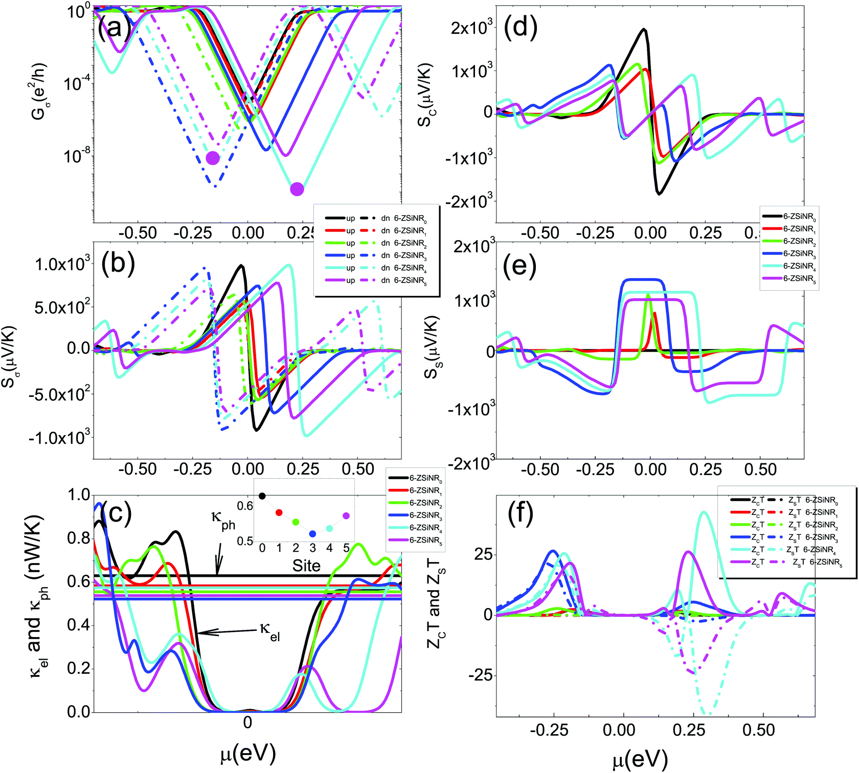
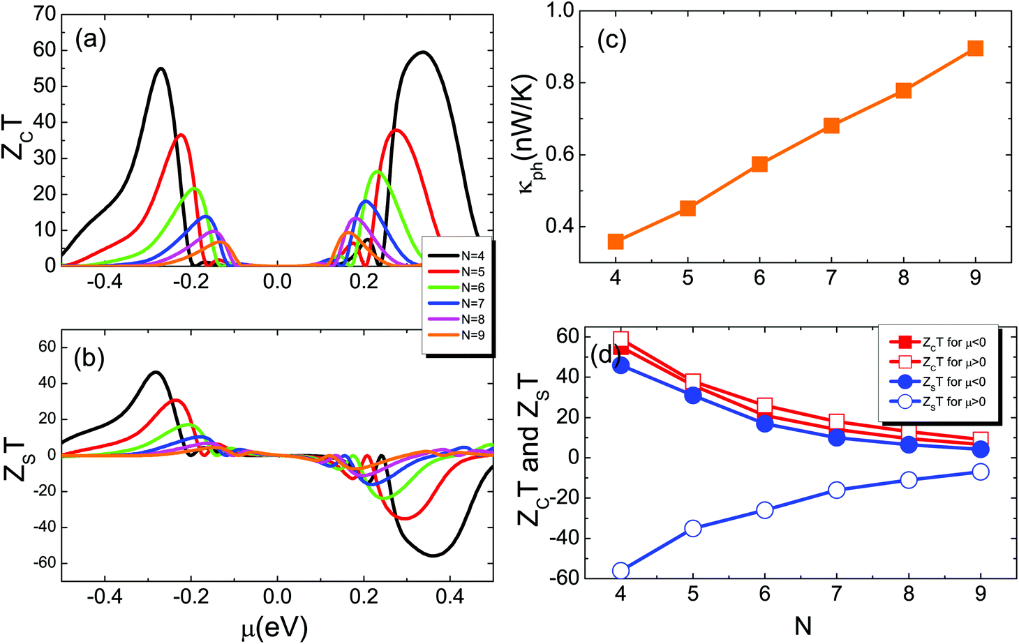
To investigate the effects of magnetic couplings between the edges on transport properties in ZSiNRs under hydrogen atom adsorption, we first examine the spin-resolved band structures of ZSiNRs with different widths, and hereafter these configurations are labelled as N-ZSiNRN−1 (here N from 4 to 9). The single hydrogen atom is adsorbed at the interedge Si atom, as shown in Fig. 5(a). The energy difference of N-ZSiNRN−1 in between the FM and AFM states is shown in Fig. 5(b). From this figure, we clearly see that though ΔEN gradually becomes smaller, it always maintains a negative value. Therefore, the FM ground state can be well maintained with the ribbon width. The energy positions of the spin-up (spin-down) CBM and spin-up (spin-down) VBM are gradually shifted towards the Fermi level as the width increases, resulting in the decrease of the spin band gap ES. These results are shown in Fig. 5(c) and (d), respectively. The spin-dependent conductance, spin-dependent Seebeck coefficient, and spin and charge Seebeck coefficients of N-ZSiNRN−1-based two-probe devices at room temperature are shown in Fig. 5. As described above in Fig. 4(a), the conductance dips appear due to the spin-dependent band gaps (see Fig. 6(a) and (b)). In the vicinity of these conductance dips, the Seebeck coefficient is obviously enhanced, as shown in Fig. 6(c) and (d). In the positive μ region close to the Fermi level, the spin-up Seebeck coefficient has a huge value, while a huge value of the spin-down Seebeck coefficient appears in the negative μ region. As a result, the charge Seebeck coefficient is dominated by the spin-up (spin-down) Seebeck coefficient above (below) the Fermi level (see Fig. 6(e)). As the width increases, the transport band gap is compressed, and the conductance dips are shifted towards the Fermi level. We also find that the peak value of the spin-dependent Seebeck coefficient decreases as the width increases, which is mainly because the conductance near the dips is enhanced with the width. The flat of SS near the Fermi level becomes narrow, and its magnitude is decreased as the ribbon increases (see Fig. 6(f)). The corresponding charge and spin thermoelectric FOMs ZCT and ZST at room temperature as a function of chemical potential are presented in Fig. 7(a) and (b), respectively. Obviously, ZCT has two positive high peaks in the vicinity of zero chemical potential. One is located above μ = 0, and the other is located below μ = 0. Similar results for ZST are also observed in Fig. 7(b), and the main difference is that one negative peak of ZST appears above μ = 0 because G↓ plays a dominant role in the chemical potential region. In addition, we also find that the maximum values of ZCT and ZST are reduced and shifted towards μ = 0, and they are also shown in Fig. 7(d). Obviously, the narrower ribbons have better thermoelectric effects than the wider ribbons. When N = 4, the maximum values of ZCT and ZST can approach 60, which is much larger than the results reported in the ZSiNRs of 2H–1H type without hydrogen adsorption.65 Here the 2H–1H type means that one edge is dihydrogenated and the other edge is monohydrogenated. In Fig. 7(c), the thermal conductance from phonon's contribution κph is plotted as a function of the width N. The results show that κph has a linear increase behavior with the width, and this is mainly because more phonon modes take part in the photonic heat transport as the width increases.
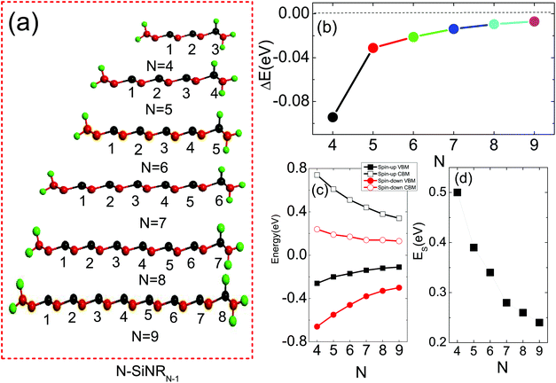 |
| | Fig. 5 (a) Atomic geometries of ZSiNRs with different widths under hydrogen adsorption. (b) The energy difference of these ZSiNRs in between the FM and AFM states versus the width. (c) The energy positions of the spin-up (spin-down) CBM and spin-up (spin-down) VBM versus the width. (d) The spin band gap versus the width. | |
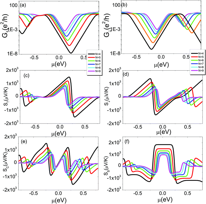 |
| | Fig. 6 (a) Spin-up conductance and (b) spin-down conductance of N-ZSiNRN−1 (N = 4, 5, 6, 7, 8, 9) versus the chemical potential. The corresponding spin-up Seebeck coefficient (c), spin-down Seebeck coefficient (d), charge Seebeck coefficient (e) and spin Seebeck coefficient versus the chemical potential at room temperature. | |
 |
| | Fig. 7 (a) ZCT and (b) ZST versus the chemical potential at room temperature. (c) The thermal conductance from phonon's contribution and (d) the maximum values of ZCT and ZST versus the width N at room temperature. | |
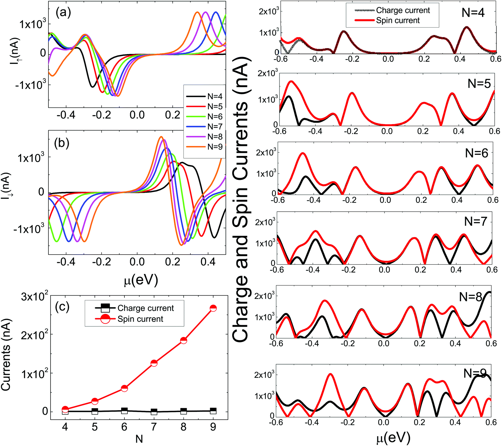
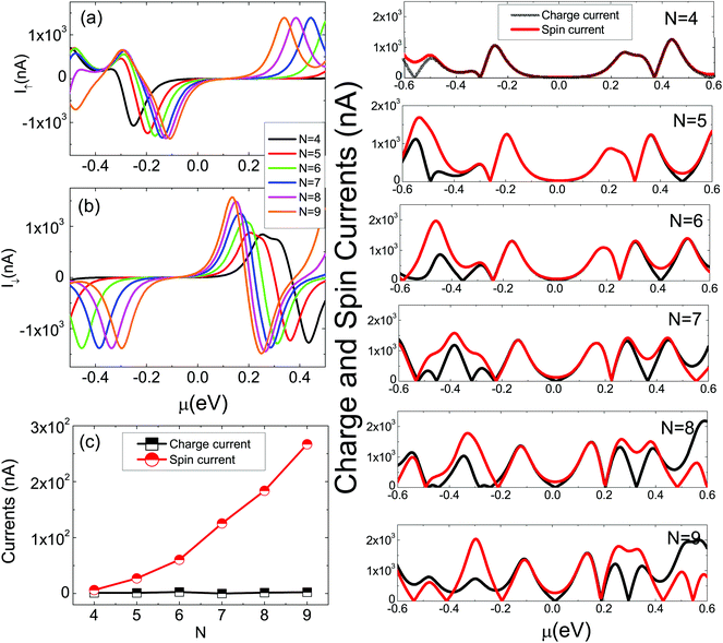
When a temperature difference ΔT is applied across the two-probe system, a thermal charge current can be generated because fL–fR is not zero. For a spin-polarized system, the thermally spin-dependent current I↑(↓) can be obtained by using eqn (1). In the linear temperature response region, the current I↑(↓) can be approximated as,70
| |  | (8) |
which clearly shows that
Iσ at
μ is determined by the spin-dependent Seebeck coefficient
Sσ and spin-dependent linear conductance
Gσ at
μ when the temperature parameters are fixed. In
Fig. 8(a) and (b), we show
I↑ and
I↓ as a function of the chemical potential
μ for Δ
T = 300 K and
T = 300 K (namely
TL = 450 K and
TR = 150 K). It is observed that the current is obviously enhanced when
μ is near the edges of transport gaps. For the spin-up current, its sign is changed from positive to negative as
μ increases in the vicinity of
μ = −0.2 V. Similar results for the spin-down current also appear in the vicinity of
μ = 0.2 V. These results can be well explained by using a simple formula
I↑, ↓ ∝
G′
↑(↓), therefore the different signs of
I↑(↓) appear in two sides of the spin-up (spin-down) conductance dips. As the width increases, the current peak values are slightly increased. In addition, the absolute values of the spin and charge currents as a function of the chemical potential
μ are shown in the right panel of
Fig. 8. From top to bottom,
N is taken from 4 to 9. As can be seen, in more
μ regions, the magnitude of
IS is nearly equal to that of
IC, which implies that the single-spin channel dominates the transport properties. In other
μ regions, we also find that
IS is larger than
IC, indicating that
I↑ and
I↓ have the opposite signs. And always,
IC is zero while
IS has a finite value in some spectral
μ points. In this case, the silicene-based device can be used to generate the pure spin current. However, since the researchers are largely concerned with the spin transport properties at the zero chemical potential, we plot
IC and
IS as a function of the width
N at
μ = 0 in
Fig. 8(c). It is interesting that
IS is gradually increased while
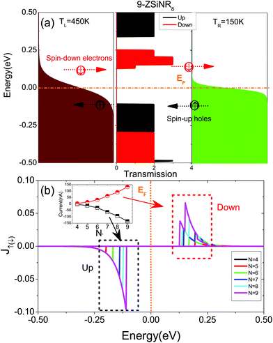
IC maintains a very low value. To reveal the underlying physical mechanism of the pure spin current, we present a theoretical model in
Fig. 9(a). As an example, the spin-resolved transmission function of 9-ZSiNR
8 is inserted in between the Fermi–Dirac distribution of the left and right electrodes. Since the temperature of the left electrode (
T = 450 K) is larger than that of the right electrode (
T = 150 K), more electrons below the Fermi level are excited to above the Fermi level in the left electrode compared with the excited electrons in the right electrodes. Such a non-equilibrium feature tends to produce the charge transport in the two-probe system. As shown in
Fig. 9(a), the spin-down thermal electrons above the Fermi level are transmitted from the left electrode to the right electrode with the help of the spin-down CB. Moreover, the spin-up thermal holes move from the right electrode to the left electrode through the spin-up VB. Thus a positive spin-down current and a negative spin-up current are generated as shown in the inset of
Fig. 9(b). The current density
J↑(↓) = (
fL −
fR)
τ↑(↓) is presented in
Fig. 9(b). Obviously, the negative spin-up current mainly comes from the peaks of
J↑ below the Fermi level, while the positive spin-down current is dominated by the spin-down peaks of
J↓ above the Fermi level. As
N increases, the width and height of these peaks of
J↑(↓) are enhanced, and then
I↑ and
I↓ are gradually increased as
N increases (see the inset of
Fig. 9(b)). Meanwhile, their magnitudes are always nearly equal, thus a nearly pure spin current is achieved at
μ = 0 in the absence of the gate voltage.
 |
| | Fig. 8 The left panel: (a) Thermally-induced spin-up current and (b) spin-down current versus the chemical potential for ΔT = 300 K and T = 300 K. (c) Spin and charge currents as a function of the width N. The right panel: The corresponding spin and charge currents versus the chemical potential at different widths. | |
 |
| | Fig. 9 (a) The theoretical model used to explain the physical mechanisms of the pure spin current. (b) The current density as a function of energy at different widths. The inset in (b) shows I↑ and I↓versus the width N. | |
4. Conclusions
In summary, we investigate the magnetic properties and spin Seebeck effects of the silicene-based devices with using first-principles methods. It is found that the ground state of ZSiNRs varies from a AFM state to a FM state by tuning the hydrogen atom adsorption site. Meanwhile a spin-degenerate semiconductor evolves into a spin semiconductor. In the narrow ZSiNRs, the spin and charge thermoelectric FOMs become almost equal, and their values approach 60, indicating that excellent spin thermoelectric properties are obtained. Using a temperature difference, a nearly pure spin current is generated, and its magnitude is gradually increased with the ribbon width.
Conflicts of interest
There are no conflicts to declare.
Acknowledgements
The authors thank the support of the National Natural Science Foundation of China (NSFC) (Grant No. 61674022), the Natural Science Foundation of Jiangsu Province (Grant No. BK20171243) and the Key Project of Natural Science Research in Colleges and Universities (Grant No. 17KJA480001). X. F. Yang and Y. S. Liu also thank the support of the Qing Lan Project of Jiangsu Province. This work is also supported by the Outstanding Scientific and Technological Innovation Team of Jiangsu Province. X. F. Yang thanks the support of the Enterprise Postdoctoral Foundation of Jiangsu Province.
References
- J. C. Zhuang, X. Xu, H. F. Feng, Z. Li, X. L. Wang and Y. Du, Sci. Bull., 2015, 60, 1551 CrossRef CAS.
- A. Gupta, T. Sakthivel and S. Seal, Prog. Mater. Sci., 2015, 73, 44 CrossRef CAS.
- J. J. Zhao, H. S. Liu, Z. M. Yu, R. G. Quhe, S. Zhou, Y. Y. Wang, C. C. Liu, H. X. Zhong, N. N. Han, J. Lu, Y. G. Yao and K. H. Wu, Prog. Mater. Sci., 2016, 83, 24 CrossRef CAS.
- S. Cahangirov, M. Topsakal, E. Aktürk, H. Sahin and S. Ciraci, Phys. Rev. Lett., 2009, 102, 236804 CrossRef CAS PubMed.
- Y. Du, J. Zhuang, J. Wang, Z. Li, H. Liu, J. Zhao, X. Xu, H. Feng, L. Chen, K. Wu, X. Wang and S. X. Dou, Sci. Adv., 2016, 2, e1600067 CrossRef PubMed.
- A. Fleurence, R. Friedlein, T. Ozaki, H. Kawai, Y. Wang and Y. Yamada-Takamura, Phys. Rev. Lett., 2012, 108, 245501 CrossRef PubMed.
- L. Meng, Y. Wang, L. Zhang, S. Du, R. Wu, L. Li, Y. Zhang, G. Li, H. Zhou, W. A. Hofer and H. J. Gao, Nano Lett., 2013, 13, 685 CrossRef CAS PubMed.
- C. C. Liu, W. Feng and Y. Yao, Phys. Rev. Lett., 2011, 107, 076802 CrossRef PubMed.
- Q. Tang and Z. Zhou, Prog. Mater. Sci., 2013, 58, 1244 CrossRef CAS.
- X. Wang, Y. Cui, T. Li, M. Lei, J. Li and Z. Wei, Adv. Opt. Mater., 2019, 7, 1801274 CrossRef.
- R. Quhe, J. Liu, J. Wu, J. Yang, Y. Wang, Q. Li, T. Li, Y. Guo, J. Yang, H. Peng, M. Lei and J. Lu, Nanoscale, 2019, 11, 532 RSC.
- S. Lin, H. Wang, X. Zhang, D. Wang, D. Zu, J. Song, Z. Liu, Y. Huang, K. Huang, N. Tao, Z. Li, X. Bai, B. Li, M. Lei, Z. Yu and H. Wu, Nano Energy, 2019, 62, 111 CrossRef CAS.
- S. Lin, H. Wang, F. Wu, Q. Wang, X. Bai, D. Zu, J. Song, D. Wang, Z. Liu, Z. Li, N. Tao, K. Huang, M. Lei, B. Li and H. Wu, npj Flexible Electron., 2019, 3, 6 CrossRef.
- S. Lin, J. C. Liu, W. Z. Li, D. Wang, Y. Huang, C. Jia, Z. W. Li, H. Y. Wang, J. N. Song, Z. L. Liu, K. Huang, Z. Zu, M. Lei, B. Hong and H. Wu, Nano Lett., 2019, 19, 6853 CrossRef CAS PubMed.
- S. Lin, X. P. Bai, H. Y. Wang, H. L. Wang, J. N. Song, K. Huang, C. Wang, N. Wang, B. Li, M. Lei and H. Wu, Adv. Mater., 2017, 29, 1703238 CrossRef PubMed.
- W. Y. Kim and Kwang S. Kim, Nat. Nanotechnol., 2008, 3, 408 CrossRef CAS PubMed.
- J. Baringhaus, M. Ruan, F. Edler, A. Tejeda, M. Sicot, A. Taleb-Ibrahimi, A. P. Li, Z. G. Jiang, E. H. Conrad, C. Berger, C. Tegenkamp and W. A. de Heer, Nature, 2014, 506, 349 CrossRef CAS PubMed.
- G. Z. Magda, X. Z. Jin, I. Hagymási, P. Vancsó, Z. Osváth, P. Nemes-Incze, C. Y. Hwang, L. P. Biró and L. Tapasztó, Nature, 2014, 514, 608 CrossRef CAS PubMed.
- C. Léandri, H. Oughaddou, B. Aufray, J. M. Gay, G. Le Lay and A. Ranguis,
et al.
, Surf. Sci., 2007, 601, 262 CrossRef.
- B. Aufray, A. Kara, S. Vizzini, H. Oughaddou, C. Léandri, B. Ealet and G. L. Lay, Appl. Phys. Lett., 2010, 96, 183102 CrossRef.
- Y. Ding and J. Ni, Appl. Phys. Lett., 2009, 95, 083115 CrossRef.
- J. Kang, F. M. Wu and J. B. Li, Appl. Phys. Lett., 2012, 100, 233122 CrossRef.
- S. Cahangirov, M. Topsakal and S. Ciraci, Phys. Rev. B: Condens. Matter Mater. Phys., 2010, 81, 195120 CrossRef.
- Y.-W. Son, M. L. Cohen and S. G. Louie, Phys. Rev. Lett., 2006, 97, 216803 CrossRef PubMed.
- H. X. Luan, C. W. Zhang, F. B. Zheng and P. J. Wang, J. Phys. Chem. C, 2013, 117, 13620 CrossRef CAS.
- Y. J. Dong, X. F. Wang, P. Vasilopoulos, M. X. Zhai and X. M. Wu, J. Phys. D: Appl. Phys., 2014, 47, 105304 CrossRef.
- X. F. Yang, X. Zhang, X. K. Hong, Y. S. Liu, J. F. Feng, X. F. Wang and C. W. Zhang, RSC Adv., 2014, 4, 48539 RSC.
- D. Zhang, M. Q. Long, L. Cui, J. Xiao and C. N. Pan, Org. Electron., 2018, 62, 253 CrossRef CAS.
- X. Q. Deng, Z. H. Zhang, G. P. Tang, Z. Q. Fan, L. Sun, C. X. Li and H. L. Zhan, Org. Electron., 2016, 37, 245 CrossRef CAS.
- Y. S. Liu, X. S. Chen and X. F. Yang, Phys. Lett. A, 2019, 383, 2492 CrossRef CAS.
- L. Pan, H. J. Liu, X. J. Tan, H. Y. Lv, J. Shi, X. F. Tang and G. Zheng, Phys. Chem. Chem. Phys., 2012, 14, 13588 RSC.
- H. Zheng, H. J. Liu, X. J. Tan, H. Y. Lv, L. Pan, J. Shi and X. F. Tang, Appl. Phys. Lett., 2012, 100, 093104 CrossRef.
- G. E. W. Bauer, E. Saitoh and B. J. van Wees, Nat. Mater., 2012, 11, 391 CrossRef CAS PubMed.
- K. Uchida, S. Takahashi, K. Harii, J. Ieda, W. Koshibae, K. Ando, S. Maekawa and E. Saitoh, Nature, 2008, 455, 778 CrossRef CAS PubMed.
- D. S. Hong, C. J. Liu, J. E. Pearson, A. Hoffmann, D. D. Fong and A. Bhattacharyaa, Appl. Phys. Lett., 2019, 114, 242403 CrossRef.
- C. Liu, S. M. Wu, J. E. Pearson, J. S. Jiang, N. d'Ambrumenil and A. Bhattacharya, Phys. Rev. B, 2018, 98, 060415(R) CrossRef.
- D. Hirobe, M. Sato, T. Kawamata, Y. Shiomi, K. Uchida, R. Iguchi, Y. Koike, S. Maekawa and E. Saitoh, Nat. Phys., 2017, 13, 30 Search PubMed.
- M. Shirdel-Havar and R. Farghadan, Phys. Rev. B, 2018, 97, 235421 CrossRef CAS.
- X. Chen, Y. Liu, B. L. Gu, W. Duan and F. Liu, Phys. Rev. B: Condens. Matter Mater. Phys., 2014, 90, 121403 CrossRef.
- Q. B. Liu, D. D. Wu and H. H. Fu, Phys. Chem. Chem. Phys., 2017, 19, 27132 RSC.
- X. F. Yang, H. L. Wang, Y. S. Chen, Y. W. Kuang, X. K. Hong, Y. S. Liu, J. F. Feng and X. F. Wang, Phys. Chem. Chem. Phys., 2015, 17, 22815 RSC.
- Y. S. Liu, X. Y. Shao, T. Shao, J. Y. Zhang, Y. W. Kuang, D. B. Zhang, Z. G. Shao, H. L. Yu, X. K. Hong, J. F. Feng, X. F. Yang, X. S. Chen and X. F. Wang, Carbon, 2016, 109, 411 CrossRef CAS.
- M. Wierzbicki, R. Swirkowicz and J. Barnaś, Phys. Rev. B: Condens. Matter Mater. Phys., 2013, 88, 235434 CrossRef.
- M. Zeng, Y. Feng and G. Liang, Nano Lett., 2011, 11, 1369 CrossRef CAS PubMed.
- Y. S. Liu, X. F. Wang and F. Chi, J. Mater. Chem. C, 2013, 1, 8046 RSC.
- M. X. Zhai, X. F. Wang, P. Vasilopoulos, Y. S. Liu, Y. J. Dong, L. Zhou, Y. J. Jiang and W. L. You, Nanoscale, 2014, 6, 11121 RSC.
- D. D. Wu, Q. B. Liu, H. H. Fu and R. Wu, Nanoscale, 2017, 9, 18334 RSC.
- H. H. Fu, D. D. Wu, L. Gu, W. Wu and R. Wu, Phys. Rev. B: Condens. Matter Mater. Phys., 2015, 92, 045418 CrossRef.
- Y. S. Liu, Y. J. Dong, J. Zhang, H. L. Yu, J. F. Feng and X. F. Yang, Nanotechnology, 2018, 29, 125201 CrossRef CAS PubMed.
- Z. F. Wang, S. Jin and F. Liu, Phys. Rev. Lett., 2013, 111, 096803 CrossRef CAS PubMed.
- Y. C. Zhao and J. Ni, Phys. Chem. Chem. Phys., 2014, 16, 15477 RSC.
- N. Gao, G. Y. Lu, Z. Wen and Q. Jiang, J. Mater. Chem. C, 2017, 5, 627 RSC.
- J. L. Qiu, H. X. Fu, Y. Xu, Q. Zhou, S. Meng, H. Li, L. Chen and K. H. Wu, ACS Nano, 2015, 9, 11192 CrossRef CAS PubMed.
- G. Kresse and J. Furthmöller, Phys. Rev. B: Condens. Matter Mater. Phys., 1999, 54, 11169 CrossRef PubMed.
- G. Kresse, Phys. Rev. B: Condens. Matter Mater. Phys., 1999, 59, 1758 CrossRef CAS.
- T. Taylor, H. Guo and J. Wang, Phys. Rev. B: Condens. Matter Mater. Phys., 2001, 63, 245407 CrossRef.
- J. Perdew, K. Burke and M. Ernerhof, Phys. Rev. Lett., 1996, 77, 3865 CrossRef CAS PubMed.
-
S. Datta, Electronic Transport in Mesoscopic Systems, Cambridge studies in semiconductor physics and microelectronic engineering, Cambridge University Press, New York, 1997 Search PubMed.
- Y. S. Liu and Y. C. Chen, Phys. Rev. B: Condens. Matter Mater. Phys., 2009, 79, 193101 CrossRef.
- B. H. Zhou, B. L. Zhou, Y. S. Zeng, M. Y. Duan and G. H. Zhou, Front. Phys., 2018, 13, 137304 CrossRef.
- B. H. Zhou, Y. F. Gao, B. L. Zhou, Y. G. Yao, G. H. Zhou and M. Hu, Phys. Lett. A, 2017, 381, 3766 CrossRef CAS.
- Y. Xu, X. B. Chen, J. S. Wang, B. L. Gu and W. H. Duan, Phys. Rev. B: Condens. Matter Mater. Phys., 2010, 81, 195425 CrossRef.
- D. Q. Fang, S. L. Zhang and H. Xu, RSC Adv., 2013, 3, 24075 RSC.
- C. Jeong, R. Kim, M. Luisier, S. Data and M. Lundstrom, J. Appl. Phys., 2010, 107, 023707 CrossRef.
- K. Zberecki, R. Swirkowicz, M. Wierzbickia and J. Barnaś, Phys. Chem. Chem. Phys., 2014, 16, 12900 RSC.
- E. H. Lieb, Phys. Rev. Lett., 1989, 62, 1201 CrossRef PubMed.
-
N. W. Ashcroft and N. D. Mermin, Solid State Physics, Saunders College, Philadelphia, 1976 Search PubMed.
- J. P. Bergfield and C. A. Stafford, Nano Lett., 2009, 9, 3072 CrossRef CAS PubMed.
- Y. S. Liu, Y. R. Chen and Y. C. Chen, ACS Nano, 2009, 3, 3497 CrossRef CAS PubMed.
- Y. S. Liu and X. F. Yang, J. Appl. Phys., 2010, 108, 023710 CrossRef.
Footnote |
| † These authors have same contributions to the paper. |
|
| This journal is © The Royal Society of Chemistry 2020 |
Click here to see how this site uses Cookies. View our privacy policy here. 
 *a
*a

 with μL = μR = μ and TL = TR = T (in this case fL = fR = f). Since the electron–phonon coupling in silicene is weak, we here ignore its contributions to the electronic and phononic transports. Thus the spin-dependent thermal conductance κel,↑(↓) from the electron's contribution is obtained by using,61

 , and the spin and charge electrical conductance are defined by GS = G↑−G↓ and GC = G↑ + G↓,38 respectively. By using the transport parameters defined above, the charge (spin) thermoelectric efficiency is characterized by the charge (spin) FOM ZC(S)T = S2CGC(S)T/(κel, ↑ + κel, ↓ + κph),38 where SC = S↑ + S↓ and SS = S↑−S↓ are the charge and spin Seebeck coefficients, respectively.