
 Open Access Article
 This Open Access Article is licensed under a Creative Commons Attribution-Non Commercial 3.0 Unported Licence
Effect of guanidinium chloride in eliminating O2− electron extraction barrier on a SnO2 surface to enhance the efficiency of perovskite solar cells†
Miao Yuab,
Lijia Chenc,
Guannan Liab,
Cunyun Xuab,
Chuanyao Luoab,
Meng Wangab,
Gang Wang ab,
Yanqing Yaoab,
Liping Liaoab,
Sam Zhangab and
Qunliang Song*ab
ab,
Yanqing Yaoab,
Liping Liaoab,
Sam Zhangab and
Qunliang Song*ab
aInstitute for Clean Energy and Advanced Materials, School of Materials and Energy, Southwest University, Chongqing 400715, P. R. China. E-mail: qlsong@swu.edu.cn
bChongqing Key Laboratory for Advanced Materials and Technologies of Clean Energy, Chongqing 400715, P. R. China
cCollege of Physics and Electronics Engineering, Chongqing Normal University, Chongqing 401331, P. R. China
First published on 21st May 2020
Abstract
Owing to their low cost, easy fabrication and excellent chemical stability properties, tin dioxide (SnO2) nanoparticles have been widely employed as an electron transfer material in many high-efficiency perovskite solar cells (PeSCs). However, the adsorbed oxygen species (i.e. O2−) on the surface of the SnO2 layer, which are induced by the annealing process under ambient environment, have always been overlooked. In general, the adsorption of oxygen creates an energy barrier at the SnO2/perovskite interface, impairing the efficiency of PeSCs. In this work, by using guanidinium (GA) chloride to modify the SnO2 surface, we have successfully improved the power conversion efficiency (PCE) of PeSCs from 15.33% (no GA-modification) to 18.46%, with a maximum fill factor of 80%. The performance enhancement is mainly attributed to the reduced energy barrier at the SnO2/perovskite interface due to the strong coupling between the GA and the adsorbed oxygen, which has been supported by the FTIR and XPS results. The strategy of reducing the charge extraction barrier by GA modification has been demonstrated to be an efficient approach to improve both the PCE and stability.
1. Introduction
The efficiency of perovskite solar cells has grown rapidly, which is inseparable from the excellent optoelectronic properties of the perovskite and the sandwich structure of the hole transport layer (HTL)/hybrid perovskite layer/electron transport layer (ETL). The ETL plays an important role.1,2 Traditionally, titanium dioxide (TiO2),3,4 zinc oxide (ZnO),5 fullerene derivatives,6 and other organic conducting materials7,8 have been employed in planar perovskite solar cells (PeSCs) as ETL, because of their wide band-gap, high transparency and large electron mobility9–11 and are thus able to effectively extract the photo-generated electrons from the perovskite layer and prevent the hole from reaching the cathode.12 Compared to these materials, tin dioxide (SnO2) is considered as a more promising ETL material owing to its even higher mobility (240 cm−2 V−1 s−1), wider bandgap (3.6–4.0 eV), better band alignment with perovskites and excellent chemical stability.13,14 However, a uniform and compact SnO2 layer obtained through atomic layer deposition (ALD),15,16 chemical bath deposition (CBD),17 pulsed laser deposition (PLD),18 etc. involves high production cost or difficulty in composition control (as in the CBD process). Solution-processed SnO2 only involves simply spin-coating of SnO2 colloidal dispersion to form an ETL on indium tin oxide (ITO) conducting glass thus attracting great interest for its simple fabrication process with superior performance.19–21However, solution-processed SnO2 requires post-sintering treatment at about (150–180 °C).22,23 Because post-sintering in oxygen-insulated glove box may cause the oxygen vacancies or defects of SnO2 due to annealing stoichiometrically balanced colloidal SnO2 in a non-oxygen environment, this sintering treatment is usually done in ambient air which inevitably leads to oxygen adsorption24,25 on the nanocrystalline SnO2 film. These ambient oxygen molecules are converted from physical adsorption to chemisorption during the annealing process by effectively extracting intrinsic electrons from SnO2 conduction band to form O2− at surface.26 Thus, a band bending and an electronic barrier between the perovskite and SnO2 interface is formed, leading to significantly reduce the conductivity of SnO2.27 Due to the negative charge of these adsorbed O2−, the transportation of photo-generated electrons in the perovskite layer to SnO2 would be hindered with more interfacial charge recombination and then the efficiency of the device will be reduced.28
In the area of SnO2− based gas sensors, surface adsorbed O2− is reduced by CO29,30, H2 (ref. 31 and 32) and C2H5OH33 etc. to gaseous O2 which can diffuse out from SnO2 surface into air. Thus, the effect of O2− can be removed by these reductions. Considering the method of chemical reduction may generate by-products of H2O34 or SnO35 on the interface of SnO2 and perovskite, the water may cause the decomposition of perovskites36–38 and SnO can acts as a p-type material.39 All these by-products will hinder charge transfer or accelerate carrier recombination. Herein, we propose and anticipate that the strong coupling of positive and negative charges can release O2− caused charge transfer barrier without impairing the crystallization of perovskite film if the cation is properly chosen.40
It is widely reported that replacing the A-site ion in perovskite by multifunctional guanidinium (GA) can improve device stability and enhance its efficiency at the same time.41–43 As a large organic cation,44 the positive charge of GA would form strong coupling with O2−, while ammonium in GA can form strong hydrogen bonds with iodide in perovskite. Consequently, GA is chosen as an interface linker, which has not been explored before, in this work to reduce O2− caused charge transfer barrier between SnO2 and perovskite.
As expected, with an interlayer of GA atop SnO2, the PCE increased from 15.33% (no GA-modification device) to 18.46%, with maximum fill factor (FF) of 80%. The characteristic absorption peak of GA and additional split peak of ammonium peak in FTIR directly confirmed that the existence of GA and the coupling effect. The XPS further revealed the chemisorbed oxygen O2− layer on the surface of SnO2 film and the interaction between GA and O2−. UPS shows that the introduction of GA onto SnO2 realigns the energy band for less charge recombination. Finally, both the conversion efficiency and the stability of PeSCs are improved. The simple GA modification in this work which was adopted to eliminate O2− caused charge transfer barrier at SnO2/perovskite interface can also be used in other area beside photovoltaic devices.
2. Experimental section
2.1. Materials
The perovskite materials, including methylammonium iodide (CH3NH3I, >99.99%), lead(II) iodide (PbI2, >99.99%) and lead(II) chloride (PbCl2, >99.99%), and hole transport materials, containing Spiro-OMeTAD, tert-butylpyridine and bis(trifluoromethane)sulfonimide lithium salt were purchased from Xi'an Polymer Light Technology Corp (China) and used without further purification. The solvent used in this work, such as N,N-dimethylformide (DMF), chlorobenzene (CB) and dimethyl sulfoxide (DMSO) were brought from Sigma-Aldrich. SnO2 colloid precursor was purchased from Alfa Aesar (tin(IV) oxide, 15% in H2O colloidal dispersion). Guanidinium (GA) chloride was obtained from Adamas (>99.5%). Perovskite precursor was prepared according to our previous report by dissolving 1.4 M CH3NH3I, 1.26 M PbI2, 0.14 M PbCl2 in a co-solvent of DMSO and DMF (vol. ratio = 9![[thin space (1/6-em)]](https://www.rsc.org/images/entities/char_2009.gif) :1) in a glove box followed by stirring overnight at room temperature.
:1) in a glove box followed by stirring overnight at room temperature.
2.2. Device fabrication
The glass/ITO substrate was firstly cleaned by deionized water with 5% detergent (Decon 90) and then washed by pure deionized water for three times in an ultrasonic cleaning machine (KQ3200DV). The SnO2 precursor prepared by diluting SnO2 (200 μL) colloid dispersion into water (1.4 mL). Then, the SnO2 precursor was spin coated on the ITO substrate at 4000 rpm for 30 s followed by annealing at 150 °C for 30 min in ambient environment. For the GA-treated device, after cooling SnO2 layer down to room temperature, the GA aqueous solution (30 mg mL−1) was spin coated on the pre-formed SnO2 layer at 6000 rpm for 30 s and annealed at 80 °C for 30 min, and then immediately transferred to nitrogen glove box. The perovskite film was prepared by two sequential spin-coatings with 400 rpm for 3 s and then 5000 rpm for 30 s. During the second step, the chlorobenzene (200 μL) was dropped on the spinning substrate for 10 s before the end of the second step. After that, the perovskite film was annealed at 50 °C for 2 min and then 85 °C for 25 min. The HTL was obtained by spin-coating the Spiro-OMeTAD solution (Spiro-OMeTAD 72.5 mg mL−1, tert-butylpyridine 28 μL mL−1 and bis(trifluoromethane)sulfonimide lithium salt 17.5 μL mL−1, 520 mg mL−1 in acetonitrile) at 5000 rpm for 30 s. Finally, 100 nm Ag electrode was thermally evaporated on top of Spiro-OMeTAD film at ≈10−6 Torr to complete the device fabrication.To prepare the SnO2/GA/wash device, all the above mentioned fabrication procedure was kept excepting the following step. In order to remove the un-binding GA molecules, the GA-treated SnO2 layer was firstly rinsed three time with deionized water followed by spin-coating of deionized water (∼80 μL) on the cleaned SnO2 film with the parameter used in perovskite film preparation. After the washing procedure, the film was dried under low temperature with nitrogen stream. In addition, to prepare the SnO2/oxygen-plasma device, the pre-formed SnO2 film was treated with oxygen plasma (30 W and 100 mTorr) for 5 minutes.
2.3. Characterization
The J–V characteristics measurement were performed by a Keithley 2400 source meter. The device was illuminated by a solar simulator Newport simulator (model 94043A) under AM 1.5 (100 mW cm−2). During the test, the J–V curves were recorded by scanning the voltage from +1.2 to −0.2 V with a voltage step of 10 mV with no delay time. External quantum efficiency (EQE) was conducted by using a lock-in amplifier (SR-830) to record the photocurrent generated from the modulated monochromatic light. The EQE of devices was calculated from the measured photocurrent and the light intensity. XPS and UPS analyses were carried out by Thermo Fisher ESCALAB 250Xi. FTIR measurements were carried out with Thermo Scientific Nicolet 6700 FTIR spectrometer, in which the wavenumber ranges from 4000 to 400 cm−1. The crystallization of the perovskite film was investigated by an XRD-7000 X-ray diffractometer from SHIMADZU, Japan with 4° min−1. The surface morphology and grain size of the perovskite films were characterized by field-emission scanning electron microscopy (SEM, JSM-6700F), UV-vis absorption spectra was tested by Shimadzu UV-2550 spectrometer.3. Results and discussion
In this work, the planar n–i–p PeSCs with structure of glass/ITO/SnO2 (or GA-modified SnO2)/MAPbI3−xClx/Spiro-OMeTAD/Ag were fabricated, as shown in Fig. 1a. The preparation of GA-modified SnO2 layer (hereafter abbreviated as SnO2/GA) was conducted by directly spin-coating the GA aqueous solution onto the pre-annealed SnO2 layer. In order to check if GA is indeed linked to SnO2 surface, Fourier transform infrared (FTIR) spectroscopy was firstly performed. As shown in Fig. 1b, no difference of absorption peaks before 1500 cm−1 are observed in both bare SnO2 and SnO2/GA films because the characteristic absorption of GA is not located in this range.45 In addition, there is no obvious absorption peak in the bare SnO2 film between 1500 and 4000 cm−1, whereas two absorption peaks are noted in the SnO2/GA film in the same wavenumber range. By zooming in and equally amplifying the absorption peaks of SnO2 and SnO2/GA films from 1500 to 4000 cm−1 (see Fig. 1c), the two main absorption peaks of SnO2/GA film are similar to that of pure guanidinium chloride film. As displayed in Fig. 1d, the absorption peaks at 1600 and 3500 cm−1 are ascribed to N–H vibrational mode and the N–H stretching mode, respectively.46 These characteristic absorption peaks observed in SnO2/GA film demonstrate that GA is indeed adsorbed on the surface of SnO2 film.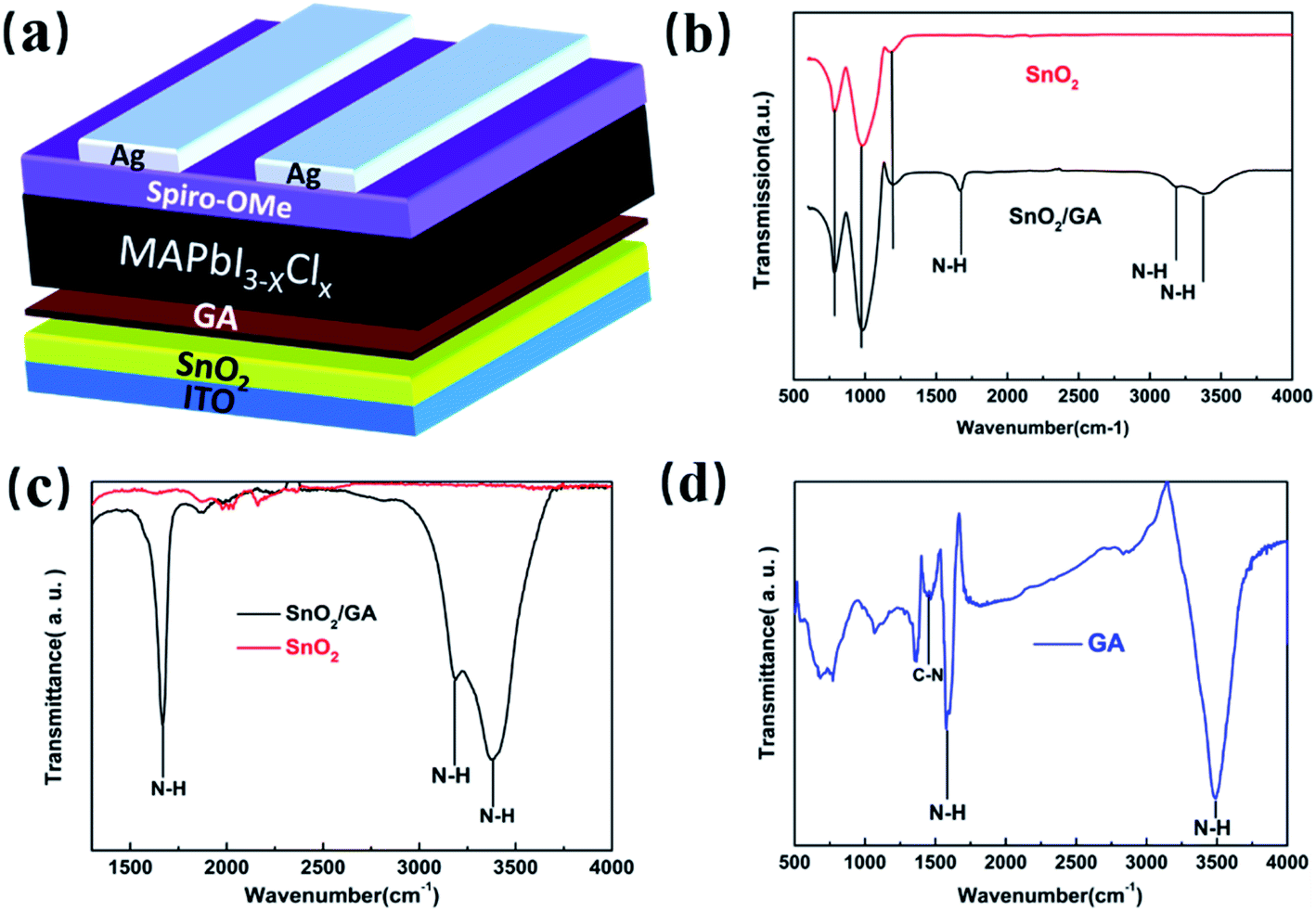 | ||
| Fig. 1 (a) Schematic device structure used in this work. (b) Fourier transform infrared (FTIR) spectroscopy of SnO2 and SnO2/GA (c) the absorption peaks of SnO2 and SnO2/GA from 1250 to 4000 cm−1 (d) FTIR spectroscopy of pure GA. | ||
However, a splitting and shifting of the absorption peak at 3500 cm−1 is observed in the SnO2/GA film when compared to that of bare SnO2 film. As evidenced in Fig. 1c, two absorption peaks are observed at 3190 and 3370 cm−1 in SnO2/GA film, respectively. Such a behaviour is mainly related to the strong coupling between GA and chemisorbed oxygen O2− on SnO2 surface. In the pure guanidinium chloride film, the positive charges are dispersed on the three nitrogen atoms and the central carbon atom,47 therefore, only one obviously stretching mode is recorded due to the conjugation of the three nitrogen atoms. However, the chemical environment of one nitrogen atom (positive charged nitrogen) in the SnO2/GA film is changed due to the coupling between GA and chemisorbed oxygen O2− on SnO2 surface. As a result, two absorption peaks are recorded in this film due to the splitting and shifting the N–H stretching mode.
To explore the influence of coupling between GA and chemisorbed oxygen O2− on the electrical performance, the planar n–i–p architecture PeSCs (see Fig. 1a) based on bare SnO2 and SnO2/GA layer with different GA-modification concentrations were fabricated and measured under 1.5 AM solar illumination. The J–V characteristics of devices with different GA-modification concentrations are depicted in Fig. S1† and their corresponding performances are listed in Table S1.† Clearly, the optimized GA-modification concentration is 0.3 mmol L−1. For clarity, the J–V characteristics of the devices based on bare SnO2 and the optimized SnO2/GA (hereafter named as bare SnO2 device and SnO2/GA device, respectively) are highlighted in Fig. 2a. For reproducibility and reliability of the results, PCE distribution histogram of 20 individual devices based on bare SnO2 and SnO2/GA is shown in Fig. S2.† Without GA modification, the devices PCE distribution was more discrete. In contrast, a narrow PCE distribution was achieved and the average efficiency increased to 18% in SnO2/GA device. The bare SnO2 device exhibits the PCE of 15.48% with an open-circuit voltage (VOC) of 1.13 V, a short-circuit current (JSC) of 19.00 mA cm−2 and a FF of 72.13%. Remarkably, the JSC and FF sharply increase in the device based on SnO2/GA ETL, with a VOC of 1.14 V, a JSC of 20.16 mA cm−2 and a FF of 80.00%, achieving a PCE of 18.46%. The enhancement of JSC is further supported by its EQE and integrated JSC. As evidenced in Fig. 2b, the integrated JSC value increases from 18.2 mA cm−2 of bare SnO2 device to 19.3 mA cm−2 of SnO2/GA device within 5% deviation in EQE. In addition, it is necessary to mention that one of SnO2/GA devices achieves a FF of 80.87% with a PCE of 18.16% (data are not shown). Up to date, it is difficult to achieve such high FF in SnO2 based PeSCs. The above results indicate that GA-modification of SnO2 film is beneficial to improve the device performance.
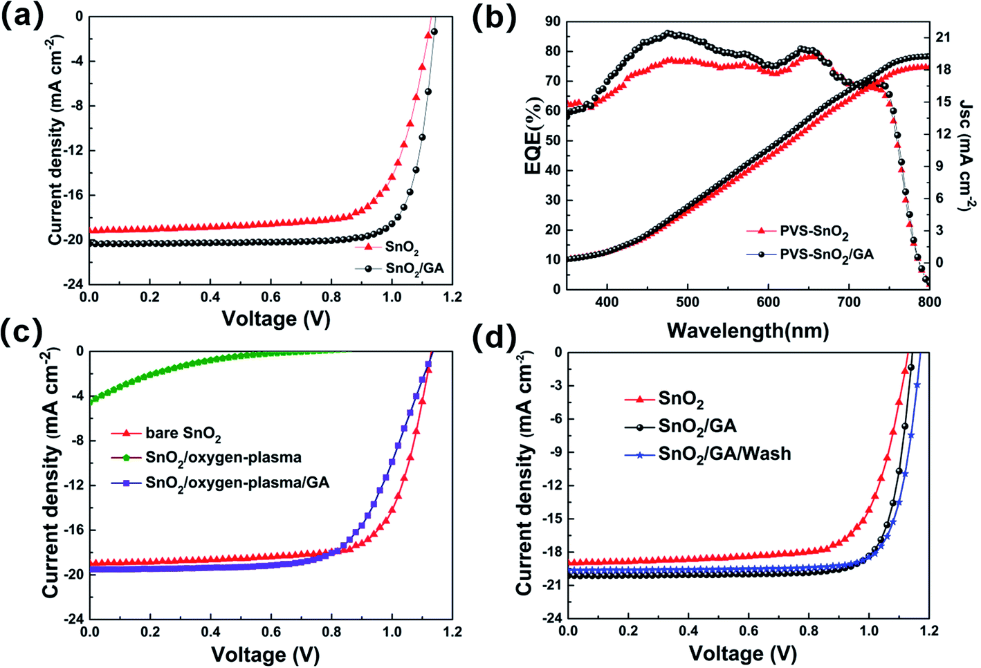 | ||
| Fig. 2 (a) J–V characteristics and (b) external quantum efficiency (EQE) spectra of device based on SnO2 and SnO2/GA ETL. (c) The comparison of J–V characteristics based on the bare SnO2 device, SnO2/oxygen device and SnO2/oxygen/GA device, respectively. (d) The J–V characteristics of bare SnO2 device, SnO2/GA device and SnO2/GA/wash device, respectively. | ||
Furthermore, a control experiment has been designed and performed aiming to further understand the influence of GA coupling with adsorption oxygen species on SnO2 surface. Three kinds of PeSCs based on different SnO2− treated ETLs have been fabricated and compared (experimental details are described in Experiment section). All other active layers are the same excepting the SnO2 layer in these three kinds of devices. The SnO2− treated methods include: (1) bare SnO2 layer (hereafter named as bare SnO2 device), (2) treating the SnO2 surface with oxygen plasma (hereafter referred to as SnO2/oxygen-plasma device) and (3) firstly treating the SnO2 surface with oxygen plasma followed by covering the oxygen plasma treated SnO2 surface with GA (hereafter abbreviated as SnO2/oxygen-plasma/GA device). The J–V characteristics of 6 independent SnO2/oxygen-plasma device and 6 independent SnO2/oxygen-plasma/GA devices are displayed in Fig. S3.† For clarity, the typical J–V curves of PeSCs based on SnO2 with different treated methods are extracted and highlighted in Fig. 2c. As anticipated, the shape of J–V curve significantly deteriorates with simultaneously decreasing of VOC, JSC and FF in the SnO2/oxygen-plasma device, and then sharply declines its PCE (the measured efficiency is only 0.3–0.6%) compared to what observed in the bare SnO2 counterpart. The above phenomenon indicates that the adsorbed oxygen species on SnO2 surface would damage the efficiency of PeSCs. In sharp contrast, the electrical performance of SnO2/oxygen-plasma device significantly increases once covering with GA layer in the SnO2/oxygen-plasma/GA device. The J–V curve changes to be plump and smooth (the purple curve in Fig. 2c). Despite its performance does not completely recover the value obtained in bare SnO2 device, the final PCE of the SnO2/oxygen-plasma/GA device reaches to ∼14%, which is far more than that of SnO2/oxygen-plasma device. Again, this finding strongly confirmed that GA-modification of SnO2 surface is beneficial to improve the device performance by coupling between GA and chemisorbed oxygen O2− on SnO2 surface.
To rule out the possible migration of GA into perovskite film during preparation, a careful cleaned procedure (details are described in Experimental section) is implemented after GA coating, which can be defined as SnO2/GA/wash device.
For comparison, the J–V characteristics of three devices, including the bare SnO2 device, SnO2/GA device and SnO2/GA/wash device, are extracted and reported in Fig. 2d. Clearly, a similar J–V curves have been observed in the last two devices, which are better than that of bare SnO2 device. In particular, the SnO2/GA/wash device exhibits a PCE of 18.72% with a VOC of 1.171 V, a JSC of 19.87 mA cm−2 and a FF of 80.47%.
Compared to the SnO2/GA device, a comparable PCE but a little increase of VOC and decrease of JSC are obtained in the SnO2/GA/wash device. Such comparable PCE in both two devices demonstrates that GA migration or doping into the perovskite film during the perovskite film preparation is insignificant. In addition, the physical origin for the increase of VOC in the SnO2/GA/wash device is not clear at this time but could be related to the better alignment of GA interlayer on top of SnO2 surface in this device.
Aiming at exploring the mechanism behind the above findings, a series of cross-checks, including contact angle measurement, scanning electron microscope (SEM), X-ray diffraction (XRD) spectra and UV-vis absorption spectra, have been carried out. First of all, the surface wettability of SnO2 layer has been significantly improved after covering GA on SnO2 surface. As shown in Fig. 3a, the contact angle of bare SnO2 layer and SnO2/GA layer are 20.09° and 4.26°, respectively. A possible explanation for the wettability improvement is the formation of strong hydrogen bonding (N–H⋯I−)37 between the amino groups of GA interlayer and iodide ions of perovskite precursor, as depicted in Fig. 3b.
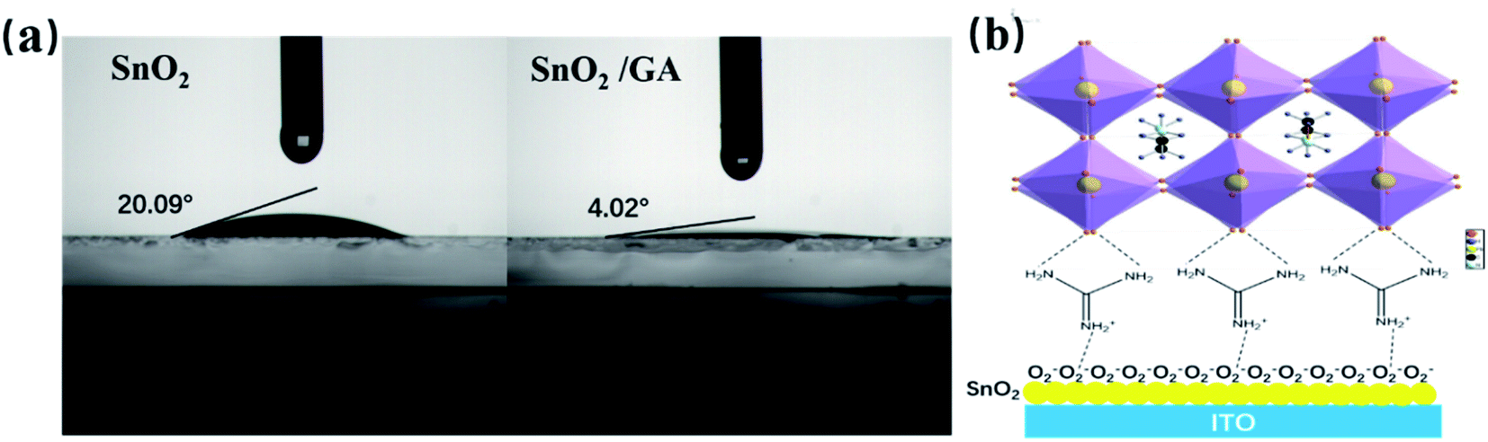 | ||
| Fig. 3 (a) Contact angle measurement of perovskite precursor on bare SnO2 layer and SnO2/GA layer, (b) schematic illustration of the covering GA on SnO2 layer. The coupling of positive charges in GA and negative charges of chemisorbed oxygen O2−, remaining two amino groups in GA interact with iodide anion in the perovskite layer. | ||
Within this context, the SEM images of perovskite films on bare SnO2 and SnO2/GA layer has been subsequently checked and the cross-sectional SEM images of perovskite films on SnO2/GA is shown in Fig. S4.† As shown in Fig. 4a, no obvious morphology differences are observed between the two kinds of perovskite films. In addition, no apparent discrepancies have been obtained in the XRD and UV-vis absorption spectra between the above two perovskite films, as evidenced in Fig. 4b and c. All the above results suggest that the covering GA interlayer on SnO2 surface has a negligible effect on the crystallization of top perovskite film and their corresponding absorption ability.
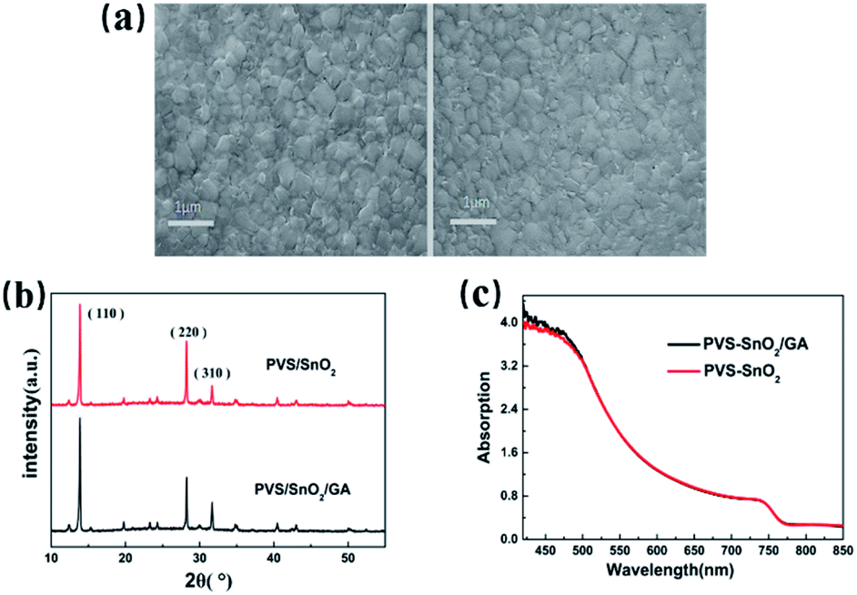 | ||
| Fig. 4 (a) SEM top-view images of perovskite active layers on (left) bare SnO2 layer and (right) SnO2/GA layer, respectively. (b) XRD spectra and (c) UV-vis absorption spectra of perovskite film on bare SnO2 layer (red curve) and SnO2/GA layer (black curve). | ||
Subsequently, X-ray photoelectron spectra (XPS) measurement has been employed to explore the accurate role of GA interlayer on the electrical performance of PeSCs. Fig. 5a and b display the asymmetric O 1s peak and their corresponding fitting curves of SnO2 film and SnO2/GA film, respectively. Clearly, after the curve-fitting procedure, the main peak (red curve) around 530.5 eV is attributed to lattice oxygen (Olatt), whereas the shoulder (blue curve) around 532.1 eV is ascribed to chemisorbed oxygen O2− related species (Ochem) at the SnO2 surface.48 Intuitively, the intensity ratio of Olatt/Ochem is slightly reduced from 1:0.39 to 1:0.30 after covering the GA interlayer on SnO2 surface due to the shielding effect of GA. In addition, the Ochem peak shifts to high binding energy after covering GA on SnO2 surface. Furthermore, a similar but small blue shift is noticed in the Sn 3d curves in SnO2/GA film when compared to that of bare SnO2 film, as shown in Fig. 5c. The two peaks at ∼486.8 and ∼495.2 eV are assigned to Sn 3d5/2 and Sn 3d3/2 in bare SnO2 film, respectively. However, the above two peaks are shifted to ∼487.1 and ∼495.5 eV in the SnO2/GA film. Again, all the above results confirm not only the presence of adsorbed oxygen on SnO2 film, but also demonstrate the interaction between GA and adsorbed oxygen on SnO2 film.
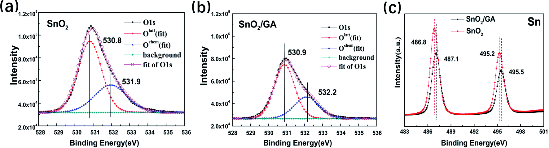 | ||
| Fig. 5 XPS spectra of the bare SnO2 film and the SnO2/GA film. O 1s spectra and its corresponding fitting curve of (a) bare SnO2 film and (b) SnO2/GA film. (c) Sn 3d spectra of bare SnO2 and SnO2/GA films. | ||
Thanks to the interaction between GA and adsorbed oxygen on SnO2 surface, the reduced of electron extraction energy barrier is expected at the SnO2/perovskite interface. Therefore, the UPS spectra has been systematically carried out on the bare SnO2, the SnO2/GA and SnO2/oxygen films. As displayed in Fig. 6a and b (the full spectra in Fig. S5†), the Fermi edge (EF,edge) are 3.49, 3.61, and 3.10 eV for SnO2, SnO2/GA, and SnO2/oxygen film, respectively. On the other hand, there is no obvious change of cut-off binding energy (Ecut-off) in the above three films. According to the following equations:
| EF = 21.22 eV − Ecut-off | (1) |
| EVB = EF − EF,edge | (2) |
| ECB = EVB + Eg | (3) |
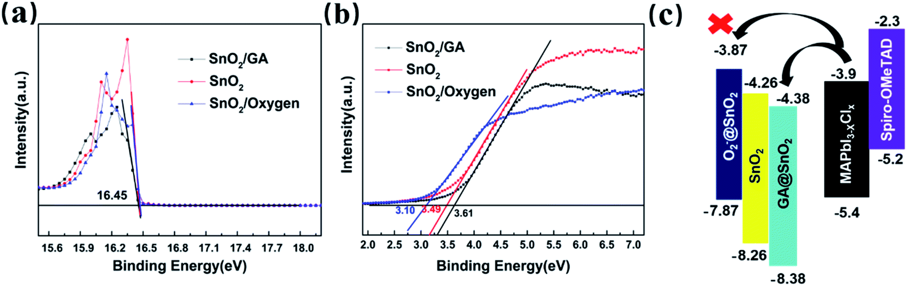 | ||
| Fig. 6 UPS spectra of the SnO2, the SnO2/GA and SnO2/oxygen film. (a) Cut-off binding energy (Ecut-off) and (b) the spectra of Fermi edge (EF,edge). (c) Schematic illustration of energy band diagram relative vacuum level of the above three kinds of SnO2-treated films. | ||
Taking this into account, we should expect to observe the increased conductivity in the SnO2/GA film. Thus, a series of samples, glass/ITO/SnO2/Au, glass/ITO/SnO2/GA/Au, glass/ITO/SnO2/oxygen-plasma/Au and glass/ITO/SnO2/oxygen-plasma/GA/Au, have been fabricated and their corresponding conductivities have been recorded and compared. As shown in Fig. 7a, the J–V curves show that the SnO2/GA samples exhibits a higher current at the same voltage than that of bare SnO2 samples. In addition, the current decreases in the SnO2/oxygen-plasma device while the current re-increases in the SnO2/oxygen-plasma/GA device. Thus, the covering of GA can obviously weaken SnO2 surface defects and improve the conductivity of SnO2. These results are consistent with the photoluminescence (PL) results based on perovskite film deposited on bare SnO2 and SnO2/GA film. As shown in Fig. 7b, the decrease of the PL intensity is observed in SnO2/GA film when compared to that of bare SnO2 film, which is attributed to the fast extraction of the carrier in the SnO2/GA case.
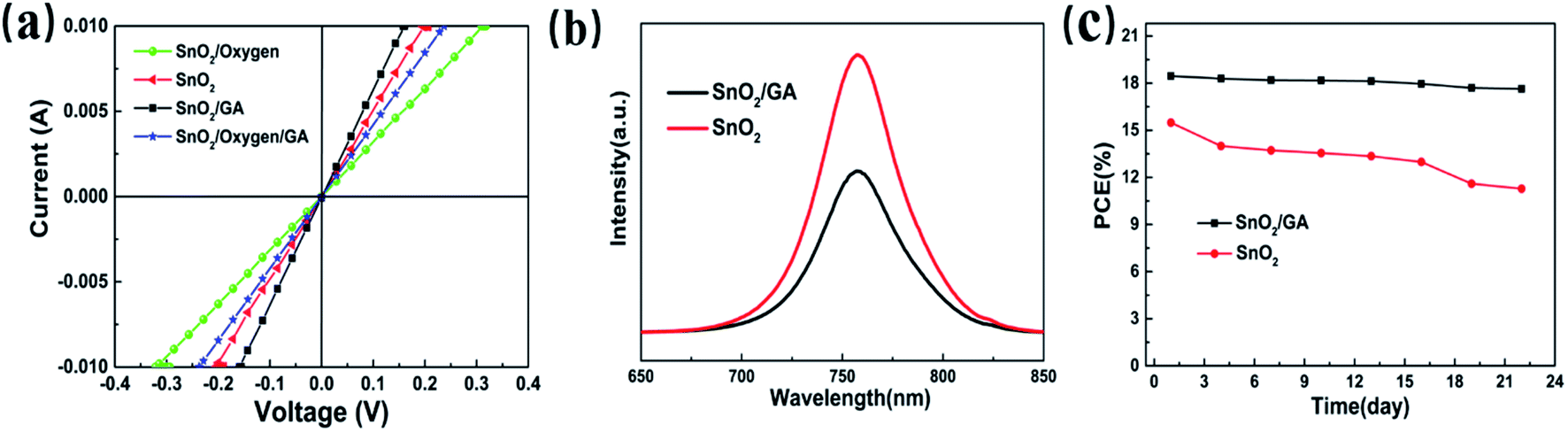 | ||
| Fig. 7 (a) J–V characteristics of SnO2 films with different surface treatments. (b) Steady-state PL of the perovskite films deposited on SnO2 and SnO2/GA film, respectively. (c) The PCE decay curve of device based on SnO2 and SnO2/GA PeSCs stored in a nitrogen-filled glovebox for 22 days. | ||
As stated before, the hydrogen bonding between GA ions and iodine ions in perovskite precursor leads to better wettability after covering GA on SnO2 surface. As anticipated, the iodine ion vacancies are inhibited, which would improve device stability. Therefore, we have investigated the shelf stability of PeSCs based on SnO2 and SnO2/GA film. The evolution of the PCE versus time of two devices is given in Fig. 7c. The SnO2/GA device maintains 95.56% of its initial value after storing 22 days in a glovebox, whereas the bare SnO2 device exhibits a relative fast degradation with ∼28% decrease of PCE in the same period. Considering this, we can safely conclude that the stability of SnO2/GA device slightly improves due to the hydrogen bonding between GA ions and iodine ions in the perovskite film.
4. Conclusion
In summary, we have systematically studied the influence of GA interlayer on the electrical performances. By covering GA interlayer on SnO2 film, the PCE of device increases from 15.33% of reference device to 18.46% of SnO2/GA device, with maximum FF of 80%. With the help of FTIR, XPS, contact angle and UPS, the roles of GA interlayer have been addressed. The GA interlayer is beneficial to reduce the energy barrier at SnO2/perovskite interface due to strong coupling between the GA and the adsorbed oxygen. Furthermore, the stability slightly increases in the SnO2/GA device caused by the suppression of iodine ion vacancies due to the strong hydrogen bonding of GA and iodide ions in perovskite precursor. This work provides a simple approach to reduce the energy barrier caused by adsorbed oxygen species for fabricating efficient and stable PeSCs.Conflicts of interest
There are no conflicts to declare.Acknowledgements
This work was supported by the National Natural Science Foundation of China (Grant No. 11774293), Chongqing Key Laboratory for Advanced Materials & Technologies of Clean Energies (JJNY201905).Notes and references
- C. Y. Xu, W. Hu, G. Wang, L. Niu, A. M. Elseman, L. Liao, Y. Yao, G. Xu, L. Luo, D. Liu, G. Zhou, P. Li and Q. L. Song, ACS Nano, 2020, 14(1), 196–203 CrossRef CAS PubMed.
- G. Wang, L. Liao, L. Niu, L. Chen, W. Li, C. Y. Xu, E. Mbeng, Y. Yao, D. Liu and Q. L. Song, Nanoscale, 2019, 11, 12108–12115 RSC.
- J. Ma, X. Guo, L. Zhou, Z. Lin, C. Zhang, Z. Yang, G. Lu, J. Chang and Y. Hao, ACS Appl. Energy Mater., 2018, 1, 3826–3834 CrossRef CAS.
- F. Giordano, A. Abate, J. P. Correa Baena, M. Saliba, T. Matsui, S. H. Im, S. M. Zakeeruddin, M. K. Nazeeruddin, A. Hagfeldt and M. Graetzel, Nat. Commun., 2016, 7, 10379 CrossRef CAS PubMed.
- J. Cao, B. Wu, R. Chen, Y. Wu, Y. Hui, B. W. Mao and N. Zheng, Adv. Mater., 2018, 30, 1705596 CrossRef PubMed.
- F. Zhang, W. Shi, J. Luo, N. Pellet, C. Yi, X. Li, X. Zhao, T. J. S. Dennis, X. Li, S. Wang, Y. Xiao, S. M. Zakeeruddin, D. Bi and M. Grätzel, Adv. Mater., 2017, 29, 1606806 CrossRef PubMed.
- C. Sun, Z. Wu, H.-L. Yip, H. Zhang, X.-F. Jiang, Q. Xue, Z. Hu, Z. Hu, Y. Shen, M. Wang, F. Huang and Y. Cao, Adv. Energy Mater., 2016, 6, 1501534 CrossRef.
- C.-Y. Chang, B.-C. Tsai, M.-Z. Lin, Y.-C. Huang and C.-S. Tsao, J. Mater. Chem. A, 2017, 5, 22824–22833 RSC.
- L. Huang and Z. Ge, Adv. Energy Mater., 2019, 9, 1900248 CrossRef.
- Z. Zhu, Y. Bai, X. Liu, C. C. Chueh, S. Yang and A. K. Jen, Adv. Mater., 2016, 28, 6478–6484 CrossRef CAS PubMed.
- Y. C. Kim, H. J. Jeong, S. T. Kim, Y. H. Song, B. Y. Kim, J. P. Kim, B. K. Kang, J. H. Yun and J. H. Jang, Nanoscale, 2020, 12, 558–562 RSC.
- W. Ke, G. Fang, Q. Liu, L. Xiong, P. Qin, H. Tao, J. Wang, H. Lei, B. Li, J. Wan, G. Yang and Y. Yan, J. Am. Chem. Soc., 2015, 137, 6730–6733 CrossRef CAS PubMed.
- H.-S. Rao, B.-X. Chen, W.-G. Li, Y.-F. Xu, H.-Y. Chen, D.-B. Kuang and C.-Y. Su, Adv. Funct. Mater., 2015, 25, 7200–7207 CrossRef CAS.
- Q. Jiang, X. Zhang and J. You, Small, 2018, 14, 1801154 CrossRef PubMed.
- S. Jeong, S. Seo, H. Park and H. Shin, Chem. Commun., 2019, 55, 2433–2436 RSC.
- Y. Lee, S. Lee, G. Seo, S. Paek, K. T. Cho, A. J. Huckaba, M. Calizzi, D. W. Choi, J. S. Park, D. Lee, H. J. Lee, A. M. Asiri and M. K. Nazeeruddin, Adv. Sci., 2018, 5, 1800130 CrossRef PubMed.
- J. Barbe, M. L. Tietze, M. Neophytou, B. Murali, E. Alarousu, A. E. Labban, M. Abulikemu, W. Yue, O. F. Mohammed, I. McCulloch, A. Amassian and S. Del Gobbo, ACS Appl. Mater. Interfaces, 2017, 9, 11828–11836 CrossRef CAS PubMed.
- N. M. Nguyen, M. Q. Luu, M. H. Nguyen, D. T. Nguyen, V. D. Bui, T. T. Truong, V. T. Pham and T. Nguyen-Tran, J. Electron. Mater., 2017, 46, 3667–3673 CrossRef CAS.
- J. Chen, X. Zhao, S. G. Kim and N. G. Park, Adv. Mater., 2019, 31, 1902902 CrossRef PubMed.
- Q. Jiang, L. Zhang, H. Wang, X. Yang, J. Meng, H. Liu, Z. Yin, J. Wu, X. Zhang and J. You, Nat. Energy, 2016, 2, 16177 CrossRef.
- J. Wei, F. Guo, X. Wang, K. Xu, M. Lei, Y. Liang, Y. Zhao and D. Xu, Adv. Mater., 2018, 30, 1805153 CrossRef PubMed.
- W. Ke, D. Zhao, A. J. Cimaroli, C. R. Grice, P. Qin, Q. Liu, L. Xiong, Y. Yan and G. Fang, J. Mater. Chem. A, 2015, 3, 24163–24168 RSC.
- A. J. Yun, J. Kim, T. Hwang and B. Park, ACS Appl. Energy Mater., 2019, 2, 3554–3560 CrossRef CAS.
- C. Wang, L. Yin, L. Zhang, D. Xiang and R. Gao, Sensors, 2010, 10, 2088–2106 CrossRef CAS PubMed.
- A. Gurlo, ChemPhysChem, 2006, 7, 2041–2052 CrossRef CAS PubMed.
- Y. F. Sun, S. B. Liu, F. L. Meng, J. Y. Liu, Z. Jin, L. T. Kong and J. H. Liu, Sensors, 2012, 12, 2610–2631 CrossRef CAS PubMed.
- M. A. Kozhushner, V. L. Bodneva, I. I. Oleynik, T. V. Belysheva, M. I. Ikim and L. I. Trakhtenberg, J. Phys. Chem. C, 2017, 121, 6940–6945 CrossRef CAS.
- J. Jiménez-López and E. Palomares, Nanoscale, 2019, 11, 20024–20029 RSC.
- Z. Lu, D. Ma, L. Yang, X. Wang, G. Xu and Z. Yang, Phys. Chem. Chem. Phys., 2014, 16, 12488–12494 RSC.
- X. Wang, H. Qin, Y. Chen and J. Hu, J. Phys. Chem. C, 2014, 118, 28548–28561 CrossRef CAS.
- G. Liu, Z. Wang, Z. Chen, S. Yang, X. Fu, R. Huang, X. Li, J. Xiong, Y. Hu and H. Gu, Sensors, 2018, 18, 949 CrossRef PubMed.
- P. G. Choi, N. Izu, N. Shirahata and Y. Masuda, ACS Omega, 2018, 3, 14592–14596 CrossRef CAS PubMed.
- T. M. Ngoc, N. Van Duy, N. Duc Hoa, C. Manh Hung, H. Nguyen and N. Van Hieu, Sens. Actuators, B, 2019, 295, 144–152 CrossRef CAS.
- M. Li, H. Zhu, G. Wei, A. He and Y. Liu, J. Mater. Sci.: Mater. Electron., 2019, 30, 19625–19638 CrossRef CAS.
- B.-E. Park, J. Park, S. Lee, S. Lee, W.-H. Kim and H. Kim, Appl. Surf. Sci., 2019, 480, 472–477 CrossRef CAS.
- A. Guerrero, J. You, C. Aranda, Y. S. Kang, G. Garcia-Belmonte, H. Zhou, J. Bisquert and Y. Yang, ACS Nano, 2016, 10, 218–224 CrossRef CAS PubMed.
- D. Wei, H. Huang, P. Cui, J. Ji, S. Dou, E. Jia, S. Sajid, M. Cui, L. Chu, Y. Li, B. Jiang and M. Li, Nanoscale, 2019, 11, 1228–1235 RSC.
- Z. Yi, N. H. Ladi, X. Shai, H. Li, Y. Shen and M. Wang, Nanoscale Adv., 2019, 1, 1276–1289 RSC.
- X. Guan, Z. Wang, M. K. Hota, H. N. Alshareef and T. Wu, Adv. Electron. Mater., 2019, 5, 1800538 CrossRef.
- Y. Ma, P. M. Hangoma, W. I. Park, J. H. Lim, Y. K. Jung, J. H. Jeong, S. H. Park and K. H. Kim, Nanoscale, 2019, 11, 170–177 RSC.
- X. Li, M. I. Dar, C. Yi, J. Luo, M. Tschumi, S. M. Zakeeruddin, M. K. Nazeeruddin, H. Han and M. Grätzel, Nat. Chem., 2015, 7, 703–711 CrossRef CAS PubMed.
- M. Long, T. Zhang, D. Chen, M. Qin, Z. Chen, L. Gong, X. Lu, F. Xie, W. Xie, J. Chen and J. Xu, ACS Energy Lett., 2019, 4, 1025–1033 CrossRef CAS.
- E. W.-G. Diau, E. Jokar and M. Rameez, ACS Energy Lett., 2019, 4, 1930–1937 CrossRef CAS.
- A. D. Jodlowski, C. Roldán-Carmona, G. Grancini, M. Salado, M. Ralaiarisoa, S. Ahmad, N. Koch, L. Camacho, G. de Miguel and M. K. Nazeeruddin, Nat. Energy, 2017, 2, 972–979 CrossRef CAS.
- D. Yang, R. Yang, K. Wang, C. Wu, X. Zhu, J. Feng, X. Ren, G. Fang, S. Priya and S. F. Liu, Nat. Commun., 2018, 9, 3239 CrossRef PubMed.
- S. Nandhini, K. Sudhakar, S. Muniyappan and P. Murugakoothan, Opt. Laser Technol., 2018, 105, 249–256 CrossRef CAS.
- N. Wang, Q. Wang, W. Lu, M. Ru and Y. Yang, J. Mol. Liq., 2019, 293, 111040 CrossRef CAS.
- B. Roose and R. H. Friend, Adv. Mater. Interfaces, 2019, 6, 1801788 CrossRef.
Footnote |
| † Electronic supplementary information (ESI) available: The J–V characteristics of devices with different GA-modification concentrations; the corresponding performance values such as VOC, JSC, FF of devices with different GA-modification concentrations; the PCE histogram of 20 bare SnO2 devices and 20 SnO2/GA devices; the J–V characteristics of 6 independent SnO2/oxygen-plasma device and 6 independent SnO2/oxygen-plasma/GA device. The full UPS spectra of the SnO2, the SnO2/GA and SnO2/oxygen film. See DOI: 10.1039/d0ra01501f |
| This journal is © The Royal Society of Chemistry 2020 |