
 Open Access Article
 This Open Access Article is licensed under a Creative Commons Attribution-Non Commercial 3.0 Unported Licence
Bandgap engineering of few-layered MoS2 with low concentrations of S vacancies†
Wen Heab,
Jia Shicd,
Hongkang Zhaoa,
Hui Wang *b,
Xinfeng Liu*c and
Xinghua Shi*bd
*b,
Xinfeng Liu*c and
Xinghua Shi*bd
aSchool of Physics, Beijing Institute of Technology, Beijing 100081, China
bLaboratory of Theoretical and Computational Nanoscience, CAS Key Laboratory for Nanosystem and Hierarchy Fabrication, CAS Center for Excellence in Nanoscience, National Center for Nanoscience and Technology, Chinese Academy of Sciences, Beijing 100190, China. E-mail: wangh@nanoctr.cn; shixh@nanoctr.cn
cCAS Key Laboratory of Standardization and Measurement for Nanotechnology, CAS Center for Excellence in Nanoscience, National Center for Nanoscience and Technology, Chinese Academy of Sciences, Beijing 100190, China. E-mail: liuxf@nanoctr.cn
dUniversity of Chinese Academy of Sciences, No. 19A Yuquan Road, Beijing 100049, China
First published on 21st April 2020
Abstract
Band-gap engineering of molybdenum disulfide (MoS2) by introducing vacancies is of particular interest owing to the potential optoelectronic applications. In this work, systematic density functional theory (DFT) calculations were carried out for few-layered 3R-MoS2 with different concentrations of S vacancies. All results revealed that the defect energy levels introduced on both sides of the Fermi level formed an intermediate band in the band gap. Both the edges of the intrinsic and intermediate bands of the structures with the same type of vacancies were generally closer to the Fermi level, and the gaps decreased as the number of layers increased from 2 to 4. The preferentially formed S vacancies at the top layer and the transition of defect types from point to line led to similar indirect band gaps for 2- and 4-layered 3R-MoS2 with a low bulk concentration (around 5%) of S vacancies. This is different from most reported results about transition metal dichalcogenide (TMD) materials that the indirect band gap decreases as the number of layers increases and the low concentrations of vacancies show negligible influence on the band gap value.
1 Introduction
Since the discovery of graphene, numerous two-dimensional (2D) materials have been synthesized and investigated. Molybdenum disulfide (MoS2), a transition metal dichalcogenide (TMD) existing mainly in 1T (tetragonal, AA stacking), 2H (hexagonal, ABAB stacking), and 3R (rhombohedral, ABCABC stacking) polymorphs, is one of the most prominent 2D materials owing to its wide potential optoelectronic applications, such as phototransistors,1 solar cells,2 light-emitting devices3 and catalysis.4–6Many experiments show that monolayer MoS2 is a direct band gap semiconductor with an optical gap of 1.9 eV3 and strong photoluminescence (PL), while multilayers exhibit much weaker PL due to their indirect band gap.7 The band gap of MoS2 decreases as the number of layers increases.7–9 The properties of MoS2 are commonly optimized by strain, doping and defect engineering.10–15 For example, both doping and defects have been reported as effective ways for the band-gap engineering of MoS2 to significantly strengthen the optical absorption.16–22 It has also been shown that low concentrations of vacancies may induce shallow and deep energy levels with negligible influence on the band gap value.23,24
Theoretically, the direct band gap is calculated to be 1.68 eV for monolayered MoS2.25 It becomes indirect and decreases as the number of layers increases.9,26,27 The optical direct band gap (at the K point) stays almost unchanged and is close to the value of the optical direct band gap of a bulk system.28 Dopants and defects can not only modulate the band gap and energy level, but also modify the compositions of the band edges.29–35 For example, point and line S vacancies can form deep or shallow gaps, induce a reduction in the band gap and even alter the electronic properties from semiconductors to metals.10,19,36
Different from the unit cell of the 1T and 2H phases, the unit cell of the 3R phase comprises triple-layer (ABC) stacking. In this way, the periodic symmetry is broken for structures with incomplete ABC stacking such as AB, ABCA, and ABCAB.37 Therefore, it is expected that 3R-type few-layered MoS2 should have different properties from the other types of MoS2.38,39 Here, considering the different distributions and concentrations of S vacancies, systemic density functional theory (DFT) calculations were carried out to study the band structure engineering of few-layered (2 to 4) 3R MoS2.
2 Computational details
All DFT calculations were performed within the generalized gradient approximation of the Perdew–Burke–Ernzerhof (PBE) functional using the Vienna ab initio simulation package (VASP).40,41 van der Waals corrections were considered for all calculations.42 An energy cut off of 500 eV for the plane-wave expansion was used and the force on the relaxed atoms was less than 0.01 eV Å−1. In the supercell, the vacuum region of 15 Å was contained in the z-direction. In the band structure calculations, the Brillouin zone was sampled using a (18 × 18 × 1) Γ-centered mesh for the unit cell,37 which has been proved to be useful in describing layered structures. The calculated values of the lattice constants for 3R bulk MoS2 were a = 3.191 Å and c = 18.530 Å, close to the experimental values (3.163 Å and 18.370 Å, respectively).43 The calculated band gap of pristine bulk 3R MoS2 was 0.80 eV, and those for 1-, 2-, 3- and 4-layered (ABCA) structures were 1.81, 1.33, 0.97 and 0.91 eV, respectively; these were in agreement with the reported experimental (1.96 and 1.55 eV for 1- and 2-layered structures, respectively)44 and calculated (1.68, 1.11, 0.93, and 0.88 eV for 1-, 2-, 3- and 4-layered structures, respectively)25,37 results. Band structure calculations with and without spin polarization were carried out for 3R MoS2 with S point vacancies, which revealed that the spin polarization had a negligible influence on the band structures. Thus, the spin polarization was not considered in this study.3 Results and discussion
To analyse the structure of 3R MoS2, the first, second and third layers of S atoms were denoted with superscripts 1, 2, and 3, and the row and column of the S atoms were denoted with subscripts i and j, respectively, as shown in Fig. 1 (e.g., nSij represents the S atom at i row and j column on the nth S layer). To study the effect of defects on the band structure of 3R MoS2, the formation energies of neutral and charged S point vacancies were calculated based on the following functions:| Ef[S] = Etot[S] − Etot[pure] − ∑nμ | (1) |
| Ef[Sq] = Etot[Sq] − Etot[pure] − ∑nμ + q[EF + Eυ + ΔV] | (2) |
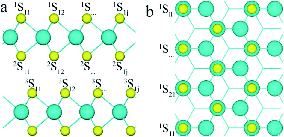 | ||
| Fig. 1 The (a) side and (b) top views of the 2-layered 3R MoS2 (the number of superscripts represents the layer of S atoms, and the first and second subscripts represent the row and column of S atoms, respectively). | ||
The formation energy of one S point defect was calculated by adopting a (6 × 6) supercell, which was large enough to avoid the influence of adjacent periodicity (dS–S = 19.15 Å), and the result (2.89 eV per S vacancy) was consistent with the reported value (2.57 eV).46 The formation energies of the negatively charged (−0.3, −1, −2e) S vacancies were calculated for 2-layered structures by the second formula. The results showed that the formation energies of the charged vacancies became larger (by 0.15, 0.64, and 1.61 eV) than that of the neutral ones and increased with the charge carried by the S vacancies; thus, they were not considered here. It should be noted that a constant chemical potential was adopted here,47,48 and the case may be different when the chemical potentials corresponding to the S (or Mo)-rich conditions were changed.49–51
For simplicity, two S point vacancies with different combinations were considered to understand the influence of the interval of S point vacancies. All models can be classified into two groups: (i) two S vacancies at the same S layer (labeled as 1S11/1Sij or 2S11/2Sij); (ii) two S vacancies at different S layers (labeled as 1S11/2Sij or 2S11/3Sij). Here, 1S11 and 2Sij were at the same Mo layer, while 2S11 and 3Sij were within different Mo layers. Different cases were considered for each group; for example, for the group (i), the 1S11 atom was combined with other 1Sij atoms in the same layer (see Fig. 1). Also, a smaller (4 × 3) (AB)-layered supercell was built to compare the tendency of the formation energies of S point vacancies in different concentrations. The formation energies are shown in Table 1.
| 1S11/1Sij (2S11/2Sij) | 1S11/2Sij | 2S11/3Sij | ||||||||||
|---|---|---|---|---|---|---|---|---|---|---|---|---|
| Distance (Å) | 3.191 | 5.527 | 6.382 | 8.882 | 9.573 | 3.115 | 4.457 | 6.343 | 3.576 | 4.793 | 5.578 | 8.595 |
| Eform (eV) | 5.75 | 5.80 | 5.83 | 5.81 | 5.81 | 5.75 | 5.88 | 5.82 | 5.85 | 5.87 | 5.87 | 5.87 |
| 5.85 | 5.91 | 5.93 (6.00) | 5.88 | 5.94 | 5.88 | 5.90 | 5.91 | 5.92 | 5.92 | |||
It was clear that the formation energy of two S point vacancies at the top layer was smaller than that for the ones with a similar distance at inner layers (5.78 vs. 5.84 eV; 5.93 vs. 6.00 eV), indicating that the structure with vacancies at the surface was more stable in energy. This was consistent with the reported results.49,50 When two vacancies were at the top layer and interacted with each other, the formation energy increased with the S–S distance (5.75 and 5.83 eV for 1S11/1S12 and 1S11/1S13, respectively), implying that the structure with the second S point vacancy closer to the first S point vacancy was more stable. When two S point vacancies were located at both sides of the Mo layer, the formation energy was regulated by their distance and sites. We noted that the formation of S point vacancies from the pristine structure inside the layers should be difficult because the S atoms needed much higher energy to get rid of the other atoms to reach the surface. However, to investigate the influence of S vacancies on the band structure of 3R MoS2 systemically, all cases were considered here.
First, the band structures of MoS2 with one S point vacancy were studied. The (3 × 3) supercell models with one S point vacancy were built for 2-, 3- and 4-layered MoS2 by removing one S atom from the model, and the point vacancies at different layers were considered. Compared with the band structure of pristine 2-layered MoS2 with an indirect band gap of 1.33 eV, the S point vacancy has a slight influence on the intrinsic band gap, while some states are introduced into the forbidden band region as the S atom is removed (see Fig. 2a). They are located on both sides of the Fermi level. One shallow occupied state around VBM and two deep unoccupied states located below CB led to an intermediate band with a gap (Eg) of 0.73 eV in the band gap. Our tests showed that S point vacancies at different layers had a slight influence on the results.
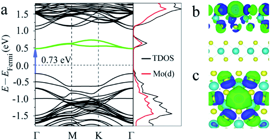 | ||
| Fig. 2 (a) Band structure, partial density of states (PDOS) and (b and c) charge-density difference for 2-layered MoS2 with one S point defect at the top S layer (side and top views). The charge density difference was calculated according to Δρdiff = ρ[MoS2] − ρ[MoS2_defect] − ρ[S]. The isosurfaces were calculated at 0.005 e Å−3. The blue and green isosurfaces represent charge depletion and accumulation regions, respectively. | ||
To obtain more insights into the influence of vacancies on the band structure of MoS2, we also calculated the partial density of states (PDOS) and charge density difference. The results showed that the states introduced into the forbidden region of the band structure were mainly contributed from the d orbitals of its neighboring Mo atoms (Fig. 2a). The charge density difference (see Fig. 2b and c) showed that charge redistributed over the whole layer with S vacancies, especially over the atoms adjacent to the defects. The free electrons provided by the S vacancies were trapped by the surrounding Mo atoms, indicating that the defect levels were spatially localized at the defect sites.
The band structure of 2-layered MoS2 with two S point vacancies was then considered. A (4 × 3) supercell was used to consider two S vacancies with different distances. The band structures for some special structures (1S11/1S12, 1S11/2S11, 1S11/2S12, and 2S11/3S11) are shown in Fig. 3a and S1.† The results were similar to that obtained with one S point vacancy. The values of the intrinsic band gaps of MoS2 showed little disturbance after the introduction of two S point vacancies, while an intermediate band with a smaller intermediate gap was introduced in the band gap.
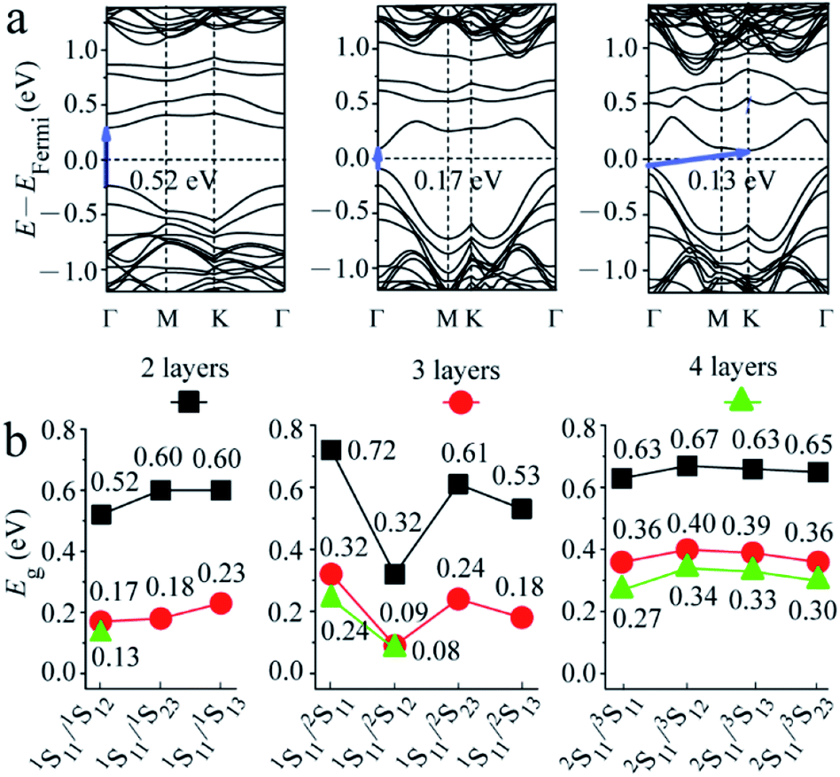 | ||
| Fig. 3 (a) Band structures for 2-, 3-, and 4-layered MoS2 with 1S11/1S12 combinational vacancies as an example and (b) the gaps of the intermediate band in the band gap (Eg) for 2-, 3-, and 4-layered MoS2 with two S vacancies at 4% bulk concentrations. | ||
The gaps of the intermediate band in the band gap for all structures are shown in Fig. 3b. It was seen that when two S atoms were removed from the top S layer of 2-layered structures, Eg increased with the S–S distance, i.e., 0.52 < 0.60 = 0.60 eV, corresponding to the distances of 3.191 (1S11/1S12), 5.527 (1S11/1S23) and 6.382 (1S11/1S13) Å. It was noted that the distance from 1S13 to 1S11 was the same as that inferred from the image of 1S11 in adjacent periodicity, i.e., the defects of 1S11/1S13 were equally distributed along one line. In summary, the smaller gap of the intermediate band in the band gap can be obtained by introducing defect levels. When the interval of two S vacancies was larger than 9.489 Å (corresponding to the 3 × 3 supercells with one S vacancy, as mentioned above), the defect levels introduced by the two S vacancies were almost at the same position. We proposed that the defect levels could be introduced at special energy positions by adjusting the distribution of vacancies.
The case becomes complicated when two S atoms are removed from the first and second S layers. There are the largest (0.72 eV (1S11/2S11)) and the smallest (0.32 eV (1S11/2S12)) (Fig. S1†) gaps of the intermediate band in 2-layered structures, corresponding to the model with two adjacent and diagonal S atoms removed from the same Mo atom. The Eg values for the model with the larger distances of 6.343 Å (1S11/2S23) and 7.100 Å (1S11/2S13) were 0.61 and 0.53 eV, respectively. It was noted that the 1S11/2S13 vacancies were evenly distributed along the a direction. In comparison, Eg for the structures with two S point vacancies at the second and third S layers showed a slight difference in values.
3- and 4-layered MoS2 materials with two S point vacancies at the same concentration were also considered for comparison by using (4 × 2) and (3 × 2) supercell models, respectively. The results (Fig. 3 and S1†) were similar to that observed for one S point defect. The intrinsic band gap of MoS2 showed little disturbance after the introduction of two S vacancies, while a smaller gap of the intermediate band in the band gap was introduced. Both gaps of the intrinsic and intermediate bands became smaller as the number of layers increased from 2 to 4 owing to the downward shift in the unoccupied energy levels and the upward shift in the occupied energy levels. However, the difference between the 3- and 4-layered structures was much smaller than that between the 2- and 3-layered structures due to the different stacking sequences (AB, ABC, and ABCA), which was similar to the tendency of pristine structures.37
As mentioned above, the point vacancies preferred to form at the top S layer and accumulated along one line, which indicated that in the experiment, the distribution of S vacancies was not homogeneous, i.e., the surface concentration of the S vacancies was much higher than that in the inner layer. Since the data obtained from experiments are generally average densities, the schematics for 2-layered MoS2 with 4S vacancies on average and at the top layer are shown in Fig. 4a and b, respectively. In this case, the surface concentration of the S vacancies was much larger (4 times). Here, we constructed n × n (n = 2, 3, …, 6) supercells for 2-layered MoS2 with one and two adjacent point vacancies and line vacancies at the top layer to investigate the effect of S vacancies on the band structures on increasing the surface concentration (0 to 50%, corresponding to the concentration from 0 to 12.5%).
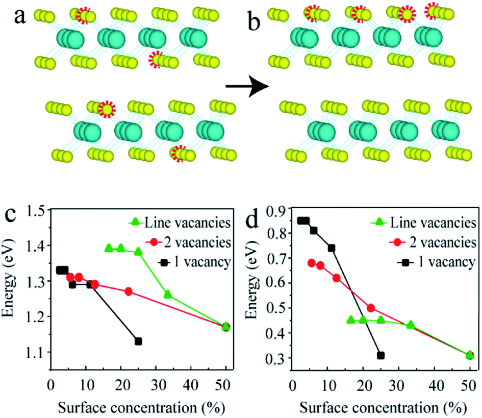 | ||
| Fig. 4 (a) Schematic diagram of vacancies on average. (b) Schematic diagram of vacancies on the top S layer. (c) The gaps of intrinsic and (d) intermediate bands in the band gaps for n × n (n = 2, 3, …, 6) supercells with one (black) and two (red) adjacent point vacancies and line (green) vacancies. | ||
The black, red and green lines in Fig. 4c and d represent the gaps of the intrinsic and intermediate bands for the models with one, two point and line vacancies, respectively. It is clear that the slopes of black, red and green lines are different, indicating that the vacancy type has a substantial influence on the band gap on increasing the vacancy concentrations. This means that the band gap decreases as the number of layers increases for few-layered structures and the difference in the structures with n and n + 1 layers becomes smaller. The phenomenon observed in our recent experiments supported this conclusion: the band gap for a 4-layered structure is equal to the value of a 2-layered structure and larger than that of a 3-layered structure.52 In addition, these results offer a variety of benefits for MoS2 material design with a tunable band gap in almost the full range between 0.08 eV and 1.8 eV.
4 Conclusions
As a typical 2D material, MoS2 has attracted significant attention due to its potential applications in electronic and optoelectronic devices. It is of particular interest that vacancies usually play an important role in tuning and modifying its various properties. In this work, we revealed the regulation of the gaps of the intrinsic and intermediate bands for 3R MoS2 with different concentrations of S point vacancies. All results showed that the gaps of both intrinsic and intermediate bands in the band gap of MoS2 decreased as the number of layers increased, while the difference for the 3- and 4-layered structures was much smaller than that for the 2- and 3-layered structures due to the different stacking sequences, which was consistent with the results for the pristine ones. For the structures with the same type and concentration of S vacancies, the band gap increased with the distance of S vacancies. As the concentration of the surface vacancies increased, the type of vacancy defects changed from point to line accordingly. These regulations of the gaps of the intrinsic and intermediate bands by S point vacancies reveal an effective way for the band-gap engineering of MoS2, opening up a direction for modulating band gaps for 2D material applications.Conflicts of interest
There are no conflicts to declare.Acknowledgements
The authors acknowledge the financial support from the National Science Foundation of Beijing (2184130) and the National Natural Science Foundation of China (11672079, 11975045).Notes and references
- Z. Yin, H. Li, H. Li, L. Jiang, Y. Shi, Y. Sun and G. Lu, ACS Nano, 2012, 6, 74–80 CrossRef CAS PubMed.
- J. Feng, X. F. Qian, C.-W. Huang and J. Li, Nat. Photonics, 2012, 6, 865–871 CrossRef.
- R. S. Sundaram, M. Engel, A. Lombardo, R. Krupke, A. C. Ferrari, P. Avouris and M. Steiner, Nano Lett., 2013, 13, 1416–1421 CrossRef CAS PubMed.
- J. Xie, H. Zhang, S. Li, R. Wang, X. Sun, M. Zhou, J. Zhou, X. W. Lou and Y. Xie, Adv. Mater., 2013, 25, 02685 Search PubMed.
- Y. Li, Y.-L. Li, C. M. Araujo, W. Luo and R. Ahuja, Catal. Sci. Technol., 2013, 3, 2214–2220 RSC.
- J. Deng, H. Li, J. Xiao, Y. Tu, D. Deng, H. Yang, H. Tian, J. Li, P. Ren and X. Bao, Energy Environ. Sci., 2015, 8, 1594–1601 RSC.
- H. S. Lee, S. W. Min, Y. G. Chang, M. K. Park, T. Nam, H. Kim, J. H. Kim, S. Ryu and S. Im, Nano Lett., 2012, 12, 3695–3700 CrossRef CAS.
- K. F. Mak, C. Lee, J. Hone, J. Shan and T. F. Heinz, Phys. Rev. Lett., 2010, 105, 136805 CrossRef PubMed.
- T. Heine, Acc. Chem. Res., 2015, 48, 65–72 CrossRef CAS PubMed.
- A. N. Enyashin, M. Bar-Sadan, L. Houben and G. Seifert, J. Phys. Chem. C, 2013, 117, 10842–10848 CrossRef CAS.
- S. B. Desai, G. Seol, J. S. Kang, H. Fang, C. Battaglia, R. Kapadia, J. W. Ager, J. Guo and A. Javey, Nano Lett., 2014, 14, 4592–4597 CrossRef CAS PubMed.
- A. P. Nayak, T. Pandey, D. Voiry, J. Liu, S. T. Moran, A. Sharma, C. Tan, C. H. Chen, L. J. Li, M. Chhowalla, J. F. Lin, A. K. Singh and D. Akinwande, Nano Lett., 2015, 15, 346–353 CrossRef CAS PubMed.
- E. Aydin, M. D. Bastiani and S. D. Wolf, Adv. Mater., 2019, 31, 1900428 CrossRef PubMed.
- O.-M. Josue, Z. Wang, C.-S. Rodolfo, M.-G. Aaron, F. Wang, X. Yao, M. Terrones and M. Endo, Adv. Mater., 2019, 31, 1805717 CrossRef PubMed.
- S. B. Ogale, Adv. Mater., 2010, 22, 3125–3155 CrossRef CAS.
- W. Zhou, X. Zou, S. Najmaei, Z. Liu, Y. Shi, J. Kong, J. Lou, P. M. Ajayan, B. I. Yakobson and J. C. Idrobo, Nano Lett., 2013, 13, 2615 CrossRef CAS PubMed.
- D. M. Sim, M. Kim, S. Yim, M.-J. Choi, J. Choi, S. Yoo and Y. S. Jung, ACS Nano, 2015, 9, 12115–12123 CrossRef CAS PubMed.
- H. Shu, Y. Li, X. Niu and J. Wang, ACS Appl. Mater. Interfaces, 2016, 8, 13150–13156 CrossRef CAS PubMed.
- S. Wang, G. D. Lee, S. Lee, E. Yoon and J. H. Warner, ACS Nano, 2016, 10, 5419–5430 CrossRef CAS.
- J. Lin, S. T. Pantelides and W. Zhou, ACS Nano, 2019, 9, 5189–5197 CrossRef PubMed.
- Y. Chen, S. Huang, X. Ji, K. Adepalli, K. Yin, X. Ling, X. Wang, J. Xue, M. Dresselhaus, J. Kong and B. Yildiz, ACS Nano, 2018, 12, 2569–2579 CrossRef CAS PubMed.
- C. Kastl, R. J. Koch, C. T. Chen, J. Eichhorn, S. Ulstrup, A. Bostwick, C. Jozwiak, T. R. Kuykendall, N. J. Borys, F. M. Toma, S. Aloni, W.-B. Alexander, R. Eli and M. S. Adam, ACS Nano, 2019, 13, 1284–1291 CAS.
- J. Jiang, C. Ling, T. Xu, W. Wang, X. Niu, A. Zafar, Z. Yan, X. Wang, Y. You, L. Sun, J. Lu, J. Wang and Z. Ni, Adv. Mater., 2018, 30, 1804332 CrossRef PubMed.
- H. Xu, X. Han, X. Dai, W. Liu, J. Wu, J. Zhu, D. Kim, G. Zou, K. A. Sablon, A. Sergeev, Z. Guo and H. Liu, Adv. Mater., 2018, 30, 1706561 CrossRef PubMed.
- P. Johari and V. B. Shenoy, ACS Nano, 2012, 6, 5449–5456 CrossRef CAS PubMed.
- J. K. Ellis, M. J. Lucero and G. E. Scuseria, Appl. Phys. Lett., 2011, 99, 261908 CrossRef.
- M.-S. Alejandro, K. Hummer and L. Wirtz, Surf. Sci. Rep., 2015, 70, 554–586 CrossRef.
- A. Kuc, N. Zibouche and T. Heine, Phys. Rev. B: Condens. Matter Mater. Phys., 2011, 83, 245213 CrossRef.
- L.-p. Feng, J. Su and Z.-t. Liu, J. Alloys Compd., 2014, 613, 122–127 CrossRef CAS.
- V. Wang, Y. Kawazoe and W. T. Geng, Phys. Rev. B: Condens. Matter Mater. Phys., 2015, 91, 045433 CrossRef.
- M. Pandey, F. A. Rasmussen, K. Kuhar, T. Olsen, K. W. Jacobsen and K. S. Thygesen, Nano Lett., 2016, 16, 2234 CrossRef CAS.
- D. Wang, W. Ju, T. Li, Q. Zhou, Z. Gao, Y. Zhang and H. Li, J. Phys. Chem. Solids, 2019, 131, 119–124 CrossRef CAS.
- S. Chen, P. Narang, H. A. Atwater and L. Wang, Adv. Mater., 2014, 26, 311–315 CrossRef CAS PubMed.
- S. Haldar, H. Vovusha, M. K. Yadav, O. Eriksson and B. Sanyal, Phys. Rev. B: Condens. Matter Mater. Phys., 2015, 92, 235408 CrossRef.
- L. Ao, H. Y. Xiao, X. Xiang, S. Li, K. Z. Liu, H. Huang and X. T. Zu, Phys. Chem. Chem. Phys., 2015, 17, 10737 RSC.
- Y. Han, T. Hu, R. Li, J. Zhou and J. Dong, Phys. Chem. Chem. Phys., 2015, 17, 3813–3819 RSC.
- X. Fan, W. T. Zheng, J. L. Kuo, D. J. Singh, C. Q. Sun and W. Zhu, Sci. Rep., 2016, 6, 24140–24148 CrossRef CAS PubMed.
- T. Cusati, A. Fortunelli, G. Fiori and G. Iannaccone, Phys. Rev. B, 2018, 98, 115403 CrossRef CAS.
- J. Park, I. W. Yeu, G. Han, C. Jang, J. Y. Kwak, C. S. Hwang and J. H. Choi, J. Phys.: Condens. Matter, 2019, 31, 315502 CrossRef CAS PubMed.
- J. P. Perdew, K. Burke and M. Ernzerhof, Phys. Rev. Lett., 1996, 77, 3865–3868 CrossRef CAS PubMed.
- G. Kresse and J. Furthmüller, Phys. Rev. B: Condens. Matter Mater. Phys., 1996, 54, 11169–11186 CrossRef CAS PubMed.
- S. Grimme, J. Comput. Chem., 2006, 27, 1787–1799 CrossRef CAS PubMed.
- B. B. Schonfeld, J. J. Huangt and S. C. Moss, Acta Crystallogr., Sect. B: Struct. Sci., 1983, 39, 404–407 CrossRef.
- K. He, C. Poole, K. F. Mak and J. Shan, Nano Lett., 2013, 13, 2931 CrossRef CAS PubMed.
- C. G. Van de Walle and J. Neugebauer, J. Appl. Phys., 2004, 2004(95), 3851–3879 CrossRef.
- S. KC, R. C. Longo, R. Addou, R. M. Wallace and K. Cho, Nanotechnology, 2014, 25, 375703 CrossRef PubMed.
- Y. Liu, K. Palotas, X. Yuan, T. j. Hou, H. p. Lin, Y. y. Li and S.-T. Lee, ACS Nano, 2017, 11, 2060–2065 CrossRef CAS PubMed.
- K. Yang, Y. Dai, B. Huang and M.-H. Whangbo, Chem. Mater., 2008, 20, 6528–6534 CrossRef CAS.
- S. Urasaki and H. Kageshima, Jpn. J. Appl. Phys., 2018, 57, 125202 CrossRef.
- L. Feng, J. Su, S. Chen and Z. Liu, Mater. Chem. Phys., 2014, 148, 5–9 CrossRef CAS.
- N. Kodama, T. Hasegawa, Y. Okawa, T. Tsuruoka, C. Joachim and M. Aono, Jpn. J. Appl. Phys., 2010, 49, 08LB01 CrossRef.
- J. Shi and X. Liu, unpublished work.
Footnote |
| † Electronic supplementary information (ESI) available: Band structures for different layered MoS2 with combinational vacancies. See DOI: 10.1039/d0ra01676d |
| This journal is © The Royal Society of Chemistry 2020 |