 Open Access Article
Effects of electrodeposition time on a manganese dioxide supercapacitor
Xiaoli Dai†
a,
Ming Zhang†a,
Jitao Li*b and
Dingyu Yang *a
*a
aCollege of Optoelectronic Technology, Chengdu University of Information Technology, Chengdu 610225, China. E-mail: jtlee@tju.edu.cn
bSchool of Precision Instruments and Optoelectronics Engineering, Tianjin University, Tianjin, 300072, China. E-mail: yangdingyu@cuit.edu.cn
First published on 21st April 2020
Abstract
As is well known that the specific capacitance of supercapacitors cannot be improved by increasing the mass of the deposited MnO2 films, which means an appropriate deposition duration is important. In this study, nanobelt-structured MnO2 films were prepared by the electrochemical deposition method under different deposition time to explore the effects of electrodeposition time change on the microstructure and electrochemical properties of this material. Benefiting from the microstructure of the MnO2 films, the transfer properties of the charged electrons and ions were promoted. Meanwhile, a 3D porous nickel foam was chosen as the deposition substrate, which rendered an enhancement of the MnO2 conductivity and the mass of the active material. The enhanced specific capacitance and specific surface area attributed to synergistic reactions. Subsequently, the electrochemical performances of the as-prepared materials were analyzed via cyclic voltammetry (CV), galvanostatic charge–discharge (GCD) and electrochemical impedance spectroscopy (EIS) tests. Results show that the optimum sample deposited for 50 s has a specific capacitance of 291.9 F g−1 at the current density of 1 A g−1 and lowest Rct. However, its electrochemical stability cannot come up to the level of the 300 s sample due to the microstructure change.
1. Introduction
As a cutting-edge technology to promote energy development in the future, the energy storage industry will play a prominent role in renewable power integration, electric vehicles, microgrids, household energy storage systems, grid support services, etc. Therefore, the energy storage technology1,2 plays a key role in the industry and its development is very meaningful. In the recent years, scientists have been paying more and more emphasis to supercapacitors, which are regarded as renewable energy storage devices due to the advantages of rapid charging and discharging, high energy density, power density, outstanding rate performance, and long-term cycling stability performance.3–6 Meanwhile, their applications in numerous fields have promising prospects, particularly in hybrid vehicles and military equipment.7,8In general, supercapacitors can be classified into two categories depending on the mechanism of energy storage – pseudocapacitors (PCs) and electric double-layer capacitors (EDLCs). However, EDLCs always show much lower specific capacitance and energy density than PCs owing to the fact that EDLCs mainly rely on the charge storage on the interface between the electrode material and the electrolyte ions.9–11 However, PCs depend on the rapid and reversible faradaic reactions that occur on the surface of the electrode material.12,13 The key to pseudocapacitors is the preparation of electrode materials. Transition metal oxides are commonly used as pseudo-capacitive materials. An electrode of hydrous RuO2 nanoparticles dispersed on the Co3O4 nanosheets with an excellent specific capacitance of 905 F g−1 at 1 A g−1 was obtained.14 However, as an electrode material, RuO2 cannot be widely used due to its high cost and rarity. In recent years, tremendous efforts have been devoted to studies on MnO2 due to its low cost, abundant natural reserve, wide potential window15,16 and green non-polluting characteristics. That shows researchers the possibility of replacing RuO2 with MnO2. However, MnO2 cannot satisfy large-scale commercial applications due to its poor conductivity17,18 and small specific surface area.19 Therefore, numerous approaches are undertaken to improve the specific capacitance of MnO2 as an electrode, such as forming a composite electrode with conductive substrates,20,21 making atomic defects22,23 and modifications.24,25 Besides, among the various methods of synthesizing MnO2, electrochemical deposition is considered to be the simplest and relatively rapid preparation method. Moreover, it is suitable for preparing nanomaterials and MnO2 with nanostructures greatly shortens the diffusion path of the electrolyte ions during the process of charging and discharging, which can effectively improve the specific capacitance of supercapacitors.26 S. S. Xiong et al. just used the MOF structure to obtain good results according to this principle.27 For instance, a granular MnO2/graphene composite was obtained via the electrochemical deposition. The specific capacitance of the best performing composite is 378 F g−1 at a scan rate of 1 mV s−1.28 Also, a flowery MnO2/graphene complex was prepared using GO and MnSO4 as the raw material via electrochemical deposition, and in a three-electrode system, the specific capacitance can reach 595.7 F g−1 at the current density of 1 A g−1.29 Previously, MnO2 with different microstructures has been successfully prepared and tested,30–35 and the results show that different structures of the same materials demonstrate different electrochemical properties. Zhu et al.36 reported a core branch heterostructure nano array of α-MnO2 nanowires and β-MnO2 ultra-thin nanosheets that combined the mass load of the active substance with enhanced pseudocapacitance. It can be seen that the performance of the material is greatly affected by the appearance of the surface, so it is very meaningful to study the microstructure of the material.
The microstructure and surface morphology of the materials are important factors affecting the properties of the material. Therefore, in this study, the changing trend of the morphology and microstructure of manganese dioxide electrode materials with time is studied. In the three-electrode system, electrochemical deposition at a constant voltage of 0.6 V is used to prepare films with different deposition time. Finally, the obtained samples were systematically tested and analyzed to decide a more appropriate deposition time. Moreover, it also contributed in laying the foundation for the subsequent improvement of experiments and the preparation of capacitors with better performance.
2. Experimental
2.1 Preparation of MnO2
The sedimentary substrate is 1.2 × 3.5 cm2 of foam nickel (110 PPI, 350 g m−2, 1 mm thick). At first, we cleaned the foam nickel (to remove the oxides that may exist on the surface) with hydrochloric acid, waterless ethanol and deionized water under ultrasonic. Then, the mass of the blank substrate was weighed after drying. Before experimenting, a mixed solution of 0.06 mol L−1 Mn(CH3COO)2 and Na2SO4 was prepared as a precursor. In a three-electrode cell, we used the as-prepared material as the working electrode, Ag/AgCl as the reference electrode and the platinum plate as the counter electrode. During the whole process, to make sure that the results are due to variation in deposition time, other parameters were kept constant and deposition time was controlled ranging from 30 s to 500 s. After the preparation, all the samples were washed with deionized water and dried in a blower box at 60 °C for 12 h. Finally, the dried samples were taken out for weighing. Both the pre-deposition and post-deposition mass was weighed with a high-precision electronic balance. The difference between the two was recorded as the quality of the MnO2 obtained from the deposition.2.2 Characterization of materials
The microstructure and surface morphology of the MnO2 films were observed via scanning electron microscopy (SEM, Zeiss ULTRA 55 SEM). The microstructure was examined via transmission electron microscopy (TEM, FEI Tecnai G2 F20) and high-resolution transmission electron microscopy (HRTEM). The chemical components on the surface were characterized via X-ray photoelectron spectroscopy (XPS) (Thermo Fisher K-Alpha 250xi).2.3 Electrochemical measurements
At room temperature, the electrochemical properties of the MnO2 films were measured on the electrochemical workstation CS350 (Wuhan Corr Test Instrument Co., Ltd.) using a 1 M Na2SO4 solution as an electrolyte.The main reaction of MnO2 during charge and discharge is
| MnO2 + Na+ + e− = MnOONa | (1) |
The mass specific capacitance of the material is calculated based on the GCD curve using the following formula:
 | (2) |
The area specific capacitance of the material is calculated via cyclic voltammetry (CV) using the following equation:
 | (3) |
 is the symbol of half of the integral area of the whole CV curve, S represents the area of the MnO2 film, Δv means the sweep rate, dV is the scan interval (potential window).
3. Results and discussion
3.1 TEM and XPS analysis
In this part, we use transmission electron microscopy to measure the crystal structure. Also, the sample with a deposition time of 50 s was selected for observation, which is sufficient to characterize other samples. As shown in Fig. 1(a and b), the crystals are composed of interlaced nanobelts with the size of about 400 nm long and 20–50 nm in diameter; the structure effectively enhanced the specific surface area for electrochemical reactions. Besides, in the HR-TEM images, we noticed two inter-planar spacings of 0.233 nm and 0.248 nm, corresponding to the (002) and (202) planes, which indicate that the crystal belongs to the orthogonal crystal system (Fig. 1(c and d)).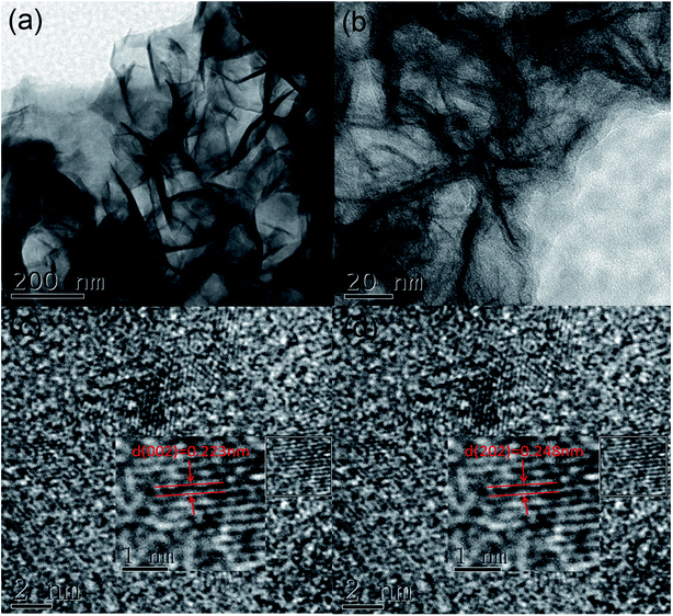 | ||
| Fig. 1 (a and b) TEM images with different magnifications; (c and d) HR-TEM images of the nanobelts of the 50 s sample. | ||
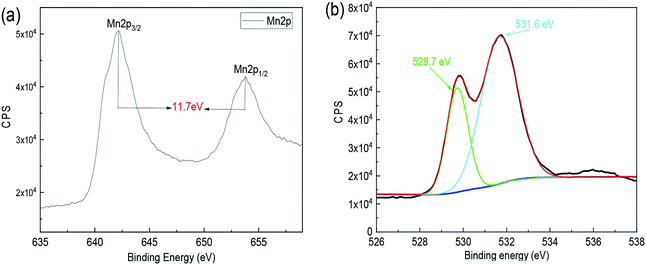
In order to investigate the oxidation states of manganese, samples were observed via X-ray photoelectron spectroscopy (XPS). Based on Fig. 2(a), two prominent peaks appeared in the Mn 2p orbit. The value of Mn 2p3/2 and Mn 2p1/2 represents Mn3+ and Mn4+, respectively. In general, the higher the chemical valence of the element Mn, the more favorable the chemical reaction is. Also, the separation value is 11.7 eV, and the result is consistent with the previous research.37 Results reveal that the element Mn is in the +4 valence state. As shown in Fig. 2(b), the O 1s spectrum was fitted, consisting mainly of two components, one is 529.7 eV (Mn–O–Mn) and the other is 531.6 eV (Mn–OH), which is in good agreement with the ref. 38–40. Hence, after comprehensive analysis, we could conclude that the deposited film is MnO2·nH2O.
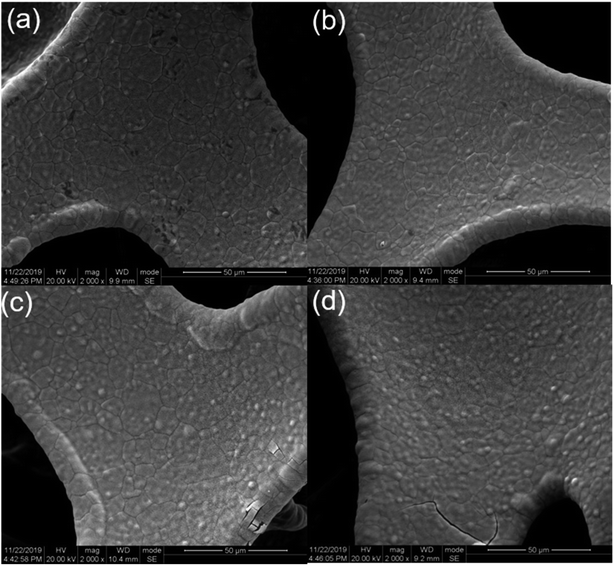
The surface topography of the electrode was observed using a scanning electron microscope. As shown in Fig. 3(b), since the continuous three-dimensional porous foam nickel substrate provided a high specific surface area for the deposition of manganese dioxide, the MnO2 films were evenly deposited on the surface of the porous nickel foam. When the deposition time increased to 300 s, as shown in Fig. 3(c), it can be seen clearly that the film has a small area of cracks, which is caused by the excessive mass load of the deposited MnO2 and the weakened bonding of the film between the substrates as the duration was extended. When the deposition time was constantly increased to 500 s, as shown in Fig. 3(d), the fracture area was dramatically increased, indicating a sustained increase in the deposited MnO2.
As shown in Fig. 3(a), 4(a and f), the MnO2 film with a deposition time of 30 s has not grown completely yet. Thus, there are still numerous small areas of the exposed substrate. As shown in Fig. 4(b–e), MnO2 with a deposition time of 50 s and 150 s grew more uniformly and the film is more complete. The MnO2 film presents a structure of similar flocs when the deposition time is increased to 300 s. However, when the deposition time increased to 500 s, the growth of MnO2 tends to be spherical with a tendency to protrude and gather. From the higher magnified scanning electron images Fig. 4(f–j), it can be observed that the manganese dioxide film with a deposition time of 30 s has a porous structure consisting of many nano-branches, and the deposited MnO2 is a single-layer structure but incomplete. MnO2 with a deposition time of 50 s still grew uniformly and completely that formed a thin and porous structure. The utilization rate of MnO2 is higher with thin and porous structures due to the electrochemical reaction occurring mainly on the surface of the substance. MnO2 with a deposition time of 150 s grew more uniformly, but the film is denser. When the deposition time increased to 300 s, MnO2 exhibits a crystallization trend. Meanwhile, the crystal volume became larger, increasing the specific surface area. Nevertheless, compared with the increase in specific surface area, the reduction in porosity and the increase in thickness have a greater impact on the decrease in mass. When the deposition time increases to 500 s, MnO2 with the nano-branches structure has a convergence trend, and the crystal volume became smaller. Therefore, the porosity and the specific surface area are reduced, which is not conducive to the transfer of electrons and ions between the active material phase and the collector interface.
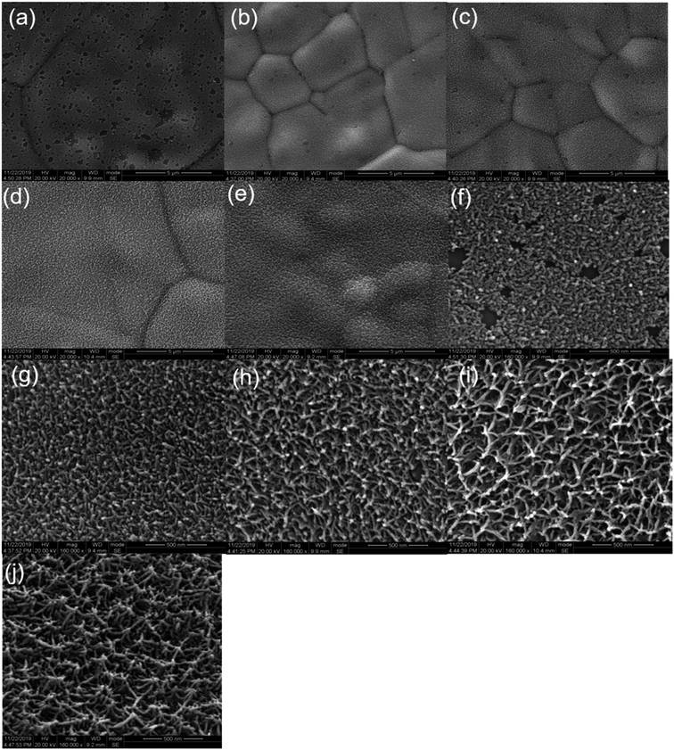 | ||
| Fig. 4 SEM images of (a) 30 s, (b) 50 s, (c) 150 s, (d) 300 s, (e) 500 s, (f) 30 s, (g) 50 s, (h) 150 s, (i) 300 s, (j) 500 s deposition time, respectively. | ||
On the basis of SEM images with different deposition time, we can find the deposition regulation of manganese dioxide during the electrochemical deposition process. At a certain potential, MnO2 is oxidized from Mn(CH3COO)2 and deposits on the substrate. The initial formation of manganese dioxide grains is very small, as deposition time increases, the grains grow up and begin to accumulate closely. Gradually, a single layer is formed by joining the local planes, which grow and spread around the points on the surface of the substrate. Also, the continuous application of voltage keeps manganese dioxide growing on its original basis. Finally, when its volume reaches a certain value, its shape changes.
3.2 Electrochemical performance
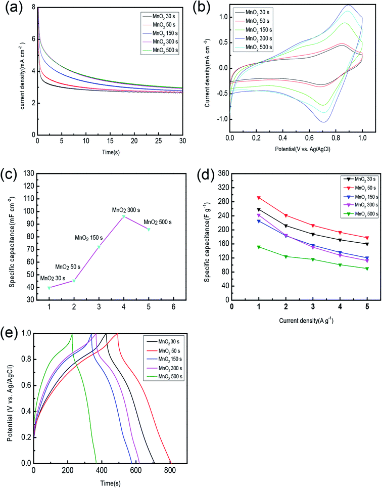
As shown in Fig. 5(a), the chronoamperometric method is used to compare the stability and electrochemical performance of the samples prepared at different deposition time. It can be seen from the diagram that the current density of all the samples at the beginning of the period is decreasing, and the drop rate in the earlier period is large, whereas in the later stage it is basically stable, in which the samples with deposition time of 300 s and 500 s decline slower, indicating that they have a more sensitive electrochemical response and more stable electrochemical properties.Fig. 5(b) shows a CV graph of different samples at a scan rate of 5 mV s−1. The CV curve shows the symmetrical curve shape of an approximate rectangle, indicating that the process is dynamically reversible. In addition, the electrode shows the pseudo capacitor characteristic of a pair of redox-reduced peaks, which is contributed by the fast and reversible reaction on the surface of the active substance. The area of the closed curve corresponding to the sample with a deposition time of 300 s is the largest, indicating that it has the maximum area specific capacitance. According to Fig. 5(c), it is obvious to see the changing trend of area specific capacitance. It happened because as the deposition time is getting longer, the mass of MnO2 deposited on the substrate is increasing. When the film thickness reached the maximum, the electrode material showed the largest area specific capacitance, whereas the area specific capacitance of the sample with the longest deposition time of 500 s is not comparable to the latter. It is possible that the changes in the microstructure of MnO2 have the opposite effect on the area specific capacitance. The results here can be explained by the SEM images.
Fig. 5(d) shows that the samples prepared by different deposition time vary in specific capacitance at different current densities. Both the deposition time and current density will affect the area specific capacitance and mass specific capacitance of the electrode. Through the figure, we can observe that the specific capacitance of the sample prepared for 50 s is the highest at any current density taken all the time. At the current density of 1 A g−1, 2 A g−1, 3 A g−1, 4 A g−1, and 5 A g−1, the specific capacitance is 291.9, 241.5, 212.8,1 92.9, and 177.9 F g−1, respectively. The reason why specific capacitance decreases with the increase in current is that active material cannot fully react at the high current density. When the deposition time is extended to 500 s, the specific capacitance is reduced to 151.5, 124.2, 116.1, 100.7, 90.2 F g−1 at a current density of 1 A g−1, 2 A g−1, 3 A g−1, 4 A g−1, and 5 A g−1, respectively. Although the film thickness increased, electrochemical reactions mainly occur on the surface of the active substance. The covered internal of the active substance cannot come into and react with the electrolyte thus being unable to contribute to the capacitance. Also, as the deposition time increases, the mass of active substance increases as well. Hence, the mass specific capacitance decreases with the increase in the deposition time. Also, the mass utilization ratio will certainly decrease.
The internal resistance of the capacitor has an extremely large effect on its electrochemical performance. If the internal resistance is small, the unnecessary heat generation during the charge and discharge process will be reduced. Fig. 5(e) presents the GCD curves at a current density of 1 A g−1 with MnO2 as the working electrode, which are distributed in a similar isosceles triangle, showing a high degree of reversibility and charge/discharge performance. It also suggests that the method of charge storage is adsorption/desorption in the electrode/electrolytic interface.41 The discharge curves of all the samples have a small voltage drop at the beginning of the output, which indicates a lower equivalent series resistance (ESR). Among all the samples, the charge–discharge performance of the samples with the deposition time of 50 s is obviously better than other samples with different deposition time. According to the GCD curve and formula (3) at a current density of 1 A g−1, the specific capacitance of the sample prepared for 30 s, 50 s, 150 s, 300 s, 500 s is calculated to be 258.4, 291.9, 225.2, 241.9, 151.5 F g−1, respectively. Compared with the CV results, it seems that we got contradictory results. However, the result calculated by the GCD method is the mass specific capacitance of the active material, while the result calculated by the CV method is the area specific capacitance of the material. Because the sample deposited in a shorter time (50 s) has less active material per unit area, it exhibits a lower area specific capacitance. The structure of the sample deposited in a short time is looser, which is conducive to the transport of electrons and ions and has a slightly smaller mass than the sample deposited for a long time. The performance of the samples with a deposition time of 30 s is inferior to that of 50 s. Here, although both of them are monolayer structures, the former deposition time is too short, which results in the insufficient quality of the deposited active material. With the extension of the deposition time, the quality of MnO2 deposited increased; the thickness of the film increased and the structure changed observably, and all the changes led to the insufficient utilization of the active material during the chemical reaction, thus its discharge time is shortened.
To further investigate the electrochemical properties of the electrode, the electrochemical impedance spectroscopy (EIS) was used to study the charge transfer dynamics and mechanisms of the supercapacitor electrode material, as shown in Fig. 6(a and b). Moreover, the equivalent circuit diagram in Fig. 6(b) is used to fit the impedance values of Rct. Obviously, as the frequency increases, the resistance R increases, and when the frequency decreases, the capacitance C strengthens. The electrochemical processes are mainly divided into dual capacitance processes and Faraday processes, which correspond to the Cdl (dual-layer capacitance) and Faraday impedance. In the high-frequency region, that is to say the arc curve, mainly charge transfer is carried out that results in Rct (charge transfer resistance). However, in the low-frequency region, mainly material transfer is carried out;36 it is shown as the approximate linear curve on the right side of the arc. The Warburg (Zw)42 impedance in this process is reflected by the slope of the curve. Furthermore, the approximate capacitance of the electrode can also be calculated by the data of the region. The electrode resistance is mainly composed of Rs (solution resistance) and Rct (charge transfer resistance). Rs is reflected by the intercept on the real axis in Fig. 6(b),42,43 including inherent resistance, ionic resistance and contact resistance of the active material to the current collector interface. The Rs of 30 s, 50 s, 150 s, 300 s and 500 s are 1.71, 1.81, 1.82, 1.80, and 1.86 Ω, respectively. The Rs of the samples with deposition time of 30 s is the lowest because the mass of the active substance is not enough to evenly distribute on the support. Besides, lower Rs also shows in the sample deposited for 50 s. While Rct can be reflected by the diameter of the semicircle in Fig. 6(b) and compared with other samples, the sample of 50 s has the smallest diameter revealing that this sample with the lowest Rct is favorable for electron and ion transport, more consistent with electrode mechanism.
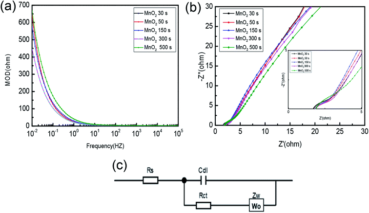 | ||
| Fig. 6 (a) Variation of impedance modulus with frequency; (b) electrochemical impedance spectroscopy; (c) equivalent model of the fitting circuit. | ||
4. Conclusion
In summary, electrochemical deposition at a constant voltage of 0.6 V was employed to prepare the composite electrodes in the form of interlaced connected tree-like nanobelts. Also, this architecture displays a number of active sites for redox reactions that promote the improvement of electrochemical properties. The microstructure of the nanomaterials was observed by SEM, which shows the changing tendency of the crystal with the extension of deposition time. Chronoamperometric response curve illustrates that the sample with a duration of 300 s has excellent chemical stability over all the as-prepared samples due to structural changes because as the deposition time increases, the accumulation of MnO2 is more compact, and the structural stability also improves. While the sample deposited for 50 s exhibits a noteworthy specific capacitance of 291.9 F g−1 at a current density of 1 A g−1 and the specific capacitance can retain up to 177.9 F g−1 when the current increased to 5 A g−1, which also has the low Rct and Rs suggesting good capacitor behavior based on the EIS analysis. In addition, during the charge and discharge process, the discharge process of this sample also lasted longer than others. Comprehensively, the optimum deposition time is 50 s because the sample shows outstanding electrochemical performances. Moreover, the present work may be a guide for the subsequent work preparing high-performance capacitors.Funding
The work was financed by the National Natural Science Foundation of China (NSFC) No. 11675029 and 51707015, and Foundation from Department of Science and Technology of Sichuan Province, China No. 2018JY0453.Conflicts of interest
There are no conflicts to declare.References
- H. Hou, C. E. Banks, M. Jing, Y. Zhang and X. Ji, Carbon quantum dots and their derivative 3D porous carbon frameworks for sodium-ion batteries with ultralong cycle life, Adv. Mater., 2015, 27, 7861–7866, DOI:10.1002/adma.201503816.
- G. Zou, H. Hou, C. W. Foster, C. E. Banks, T. Guo, Y. Jiang, Y. Zhang and X. Ji, Advanced hierarchical vesicular carbon Co-doped with S, P, N for high-rate sodium storage, Adv. Sci., 2018, 5, 1800241, DOI:10.1002/advs.201800241.
- Y. Han, N. Liu, N. Wang, Z. He and Q. Liu, Assembly of Ni–Al layered double hydroxide and oxide graphene quantum dots for supercapacitors, J. Mater. Res, 2018, 33, 4215–4223, DOI:10.1557/jmr.2018.424.
- Y. Li, Q. Li, S. Zhao, C. Chen, J. Zhou, K. Tao and L. Han, Conductive 2D Metal-Organic Frameworks Decorated on Layered Double Hydroxides Nanoflower Surface for High-Performance Supercapacitor, ChemistrySelect, 2018, 3, 13596–13602, DOI:10.1002/slct.201803150.
- M. Zhang, Y. Chen, D. Y. Yang and J. Li, High performance MnO2 supercapacitor material prepared by modified electrodeposition method with different electrodeposition voltages, J. Energy Storage, 2020, 29 DOI:10.1016/j.est.2020.101363.
- M. Zhang, X. L. Dai, C. X. Zhang, Y. W. Fuan, D. Y. Yang and J. T. Li, High Specific Capacitance of the Electrodeposited MnO2 on Porous Foam Nickel Soaked in Alcohol and its Dependence on Precursor Concentration, Materials, 2020, 13, 181, DOI:10.3390/ma13010181.
- L. L. Zhang and X. S. Zhao, Carbon-based materials as supercapacitor electrodes, Chem. Soc. Rev., 2009, 38, 2520–2531, DOI:10.1002/chin.200947213.
- J. R. Miller and P. Simon, Materials Science: Electrochemical capacitors for energy management, Science, 2008, 321, 651–652, DOI:10.1126/science.1158736.
- D. G. Lee, Y. A. Kim and B.-H. Kim, Capacitive properties of hierarchically structured carbon nanofiber/graphene/MnO2 hybrid electrode with nitrogen and oxygen heteroatoms, Carbon, 2016, 107, 783–791, DOI:10.1016/j.carbon.2016.06.093.
- Y. Xu, J. Wei, L. Tan, J. Yu and Y. Chen, A facile approach to NiCoO2 intimately standing on nitrogen doped graphene sheets by one-step hydrothermal synthesis for supercapacitors, J. Mater. Chem. A, 2015, 3, 7121–7131, 10.1039/c5ta00298b.
- C. Tanggarnjanavalukul, N. Phattharasupakun, K. Kongpatpanich and M. Sawangphruk, Charge storage performances and mechanisms of MnO2 nanospheres, nanorods, nanotubes and nanosheets, Nanoscale, 2017, 9, 13630–13639, 10.1039/c7nr02554h.
- L. Mi, W. Wei, S. Huang, S. Cui, W. Zhang, H. Hou and W. Chen, A nest-like Ni@ Ni1.4Co1.6S2 electrode for flexible high-performance rolling supercapacitor device design, J. Mater. Chem. A, 2015, 3, 20973–20982, 10.1039/c5ta06265a.
- W. Wei, S. Cui, L. Ding, L. Mi, W. Chen and X. Hu, Urchin-like Ni1/3Co2/3(CO3)1/2(OH)·0.11H2O for ultrahigh-rate electrochemical supercapacitors: structural evolution from solid to hollow, ACS Appl. Mater. Interfaces, 2017, 9, 40655–40670, DOI:10.1021/acsami.7b12392.
- R. B. Rakhi, W. Chen, M. N. Hedhili, D. Cha and H. N. Alshareef, Enhanced rate performance of mesoporous Co3O4 nanosheet supercapacitor electrodes by hydrous RuO2 nanoparticle decoration, ACS Appl. Mater. Interfaces, 2014, 6, 4196–4206, DOI:10.1021/am405849n.
- J. Wang, F. Kang and B. Wei, Engineering of MnO2-based nanocomposites for high-performance supercapacitors, Prog. Mater. Sci., 2015, 74, 51–124, DOI:10.1016/j.pmatsci.2015.04.003.
- W. Wei, X. Cui, W. Chen and D. G. Ivey, Manganese oxide-based materials as electrochemical supercapacitor electrodes, Chem. Soc. Rev., 2011, 40, 1697–1721, 10.1039/C0CS00127A.
- Q. Gao, J. Wang, B. Ke, J. Wang and Y. Li, Fe doped δ-MnO2 nanoneedles as advanced supercapacitor electrodes, Ceram. Int., 2018, 44, 18770–18775, DOI:10.1016/j.ceramint.2018.07.108.
- J. Chen, Y. Huang, X. Zhang, X. Chen and C. Li, MnO2 grown in situ on graphene@CNTs as electrode materials for supercapacitors, Ceram. Int., 2015, 41, 12680–12685, DOI:10.1016/j.ceramint.2015.06.099.
- G. P. Ojha, B. Pant, S.-J. Park, M. Park and H.-Y. Kim, Synthesis and characterization of reduced graphene oxide decorated with CeO2-doped MnO2 nanorods for supercapacitor applications, J. Colloid Interface Sci., 2017, 494, 338–344, DOI:10.1016/j.jcis.2017.01.100.
- H. Jia, Y. Cai, X. Zheng, J. Lin, H. Liang, J. Qi, J. Cao, J. Feng and W. Fei, Mesostructured carbon nanotube-on-MnO2 nanosheet composite for high performance supercapacitors, ACS Appl. Mater. Interfaces, 2018, 10, 38963–38969, DOI:10.1021/acsami.8b14109.
- H. Jia, Y. Cai, J. Lin, H. Liang, J. Qi, J. Cao, J. Feng and W. Fei, Heterostructural graphene quantum dot/MnO2 nanosheets toward high-potential window electrodes for high-performance supercapacitors, Adv. Sci., 2018, 5(5), 1700887, DOI:10.1002/advs.201700887.
- M. Khan, M. Erementchouk, J. Hendrickson and M. N. Leuenberger, Electronic and optical properties of vacancy defects in single-layer transition metal dichalcogenides, Phys. Rev. B, 2017, 95, 245435, DOI:10.1103/physrevb.95.245435.
- L. Hu, T. Zhu, X. Liu and X. Zhao, Point defect engineering of high-performance Bismuth-Telluride-based thermoelectric materials, Adv. Funct. Mater., 2014, 24, 5211–5218, DOI:10.1002/adfm.201400474.
- X. W. Sun, M. Y. Gan, L. Ma and H. H. Wang, Fabrication of PANI-coated honeycomb-like MnO2 nanospheres with enhanced electro-chemical performance for energy storage, Electrochim. Acta, 2015, 180, 977–982, DOI:10.1016/j.electacta.2015.09.056.
- L. Benhaddad, M. C. Bernard, C. Deslouis, L. Makhloufi, B. Messaoudi, A. Pailleret and H. Takenouti, Chemical synthesis of hollow sea urchin like nanostructured polypyrrole particles through a core-shell redox mechanism using a MnO2 powder as oxidizing agent and sacrificial nanostructured template, Synth. Met., 2013, 175, 192–199, DOI:10.1016/j.synthmet.2013.05.010.
- M. Kim, Y. Hwang and J. Kim, Graphene/MnO2-based composites reduced via different chemical agents for supercapacitors, Power Sources, 2013, 239, 225, DOI:10.1016/j.jpowsour.2013.03.146.
- S. S. Xiong, S. Y. Jiang, J. Wang, H. J. Lin, M. X. Lin, S. T. Weng, S. Liu, Y. Jiao, Y. C. Xu and J. R. Chen, A high-performance hybrid supercapacitor with NiO derived NiO@Ni-MOF composite electrodes, Electrochim. Acta, 2020, 340, 135956, DOI:10.1016/j.electacta.2020.135956.
- P. Y. Chan, Rusi and S. R. Majid, RGO-wrapped MnO2 composite electrode for supercapacitor application, Solid State Ionics, 2014, 262, 226–229, DOI:10.1016/j.ssi.2013.10.013.
- T. Liu, G. J. Shao, M. Ji and G. J. Wang, Synthesis of MnO2-graphene composites with enhanced supercapacitive performance via pulse electrodeposition under supergravity field, Solid State Chem., 2014, 215, 160, DOI:10.1016/j.jssc.2014.03.043.
- S. Sankar, A. I. Inamdar, H. Im, S. Lee and D. Y. Kim, Template-free rapid sonochemical synthesis of spherical α-MnO2 nanoparticles for high-energy supercapacitor electrode, Ceram. Int., 2018, 44, 17514–17521, DOI:10.1016/j.ceramint.2018.05.207.
- N. Kumar, A. Sen, K. Rajendran, R. Rameshbabu, J. Ragupathi, H. A. Therese and T. Maiyalagan, Morphology and phase tuning of α- and β-MnO2 nanocacti evolved at varying modes of acid count for their well-coordinated energy storage and visible-light-driven photocatalytic behaviour, RSC Adv., 2017, 7, 25041–25053, 10.1039/c7ra02013a.
- E. R. Ezeigwe, M. T. T. Tan, P. S. Khiew and C. W. Siong, Solvothermal synthesis of graphene–MnO2 nanocomposites and their electrochemical behavior, Ceram. Int., 2015, 41, 11418–11427, DOI:10.1016/j.ceramint.2015.05.105.
- A. Soam, K. Parida, R. Kumar, P. Kavle and R. O. Dusane, Silicon-MnO2 core-shell nanowires as electrodes for micro-supercapacitor application, Ceram. Int., 2019, 45, 18914–18923, DOI:10.1016/j.ceramint.2019.06.127.
- M. Sugantha, P. A. Ramakrishnan, A. M. Hermann, C. P. Warmsingh and D. S. Ginley, Nanostructured MnO2 for Li batteries, Int. J. Hydrogen Energy, 2003, 28, 597–600, DOI:10.1016/s0360-3199(02)00148-9.
- H. Z. Chi, H. Zhu and L. Gao, Boron-doped MnO2/carbon fiber composite electrode for supercapacitor, J. Alloys Compd., 2015, 645, 199–205, DOI:10.1016/j.jallcom.2015.05.014.
- X. Liu, G. Du, J. L. Zhu, Z. F. Zeng and X. H. Thu, NiO/LaNiO3 film electrode with binder-free for high performance supercapacitor, Appl. Surf. Sci., 2016, 384, 92–98, DOI:10.1016/j.apsusc.2016.05.005.
- G. H. A. Therese and P. V. Kamath, Electrochemical synthesis of metal oxides and hydroxides, Chem. Mater., 2000, 12, 1195, DOI:10.1021/ar00138a004.
- J. Yan, Z. J. Fan, T. Wei, W. Z. Qian, M. L. Zhang and F. Wei, Fast and reversible surface redox reaction of graphene-MnO2 composites as supercapacitor electrodes, Carbon, 2010, 48, 3825–3833, DOI:10.1016/j.carbon.2010.06.047.
- W. M. Yu, Y. Liu, L. G. Shen, Y. C. Xu, R. J. Li, T. Y. Sun and H. J. Lin, Magnetic field assisted preparation of PES-Ni@MWCNTs membrane with enhanced permeability and antifouling performance, Chemosphere, 2019, 243, 125446, DOI:10.1016/j.chemosphere.2019.125446.
- W. Yu, Y. Liu, Y. Xu, R. Li, J. Chen, B.-Q. Liao, L. Shen and H. Lin, A conductive PVDF-Ni membrane with superior rejection, permeance and antifouling ability via electric assisted in situ aeration for dye separation, J. Membr. Sci., 2019, 581, 401–412, DOI:10.1016/j.memsci.2019.03.083.
- B. J. Yoon, S. H. Jeong, K. H. Lee, H. S. Kim, C. G. Park and J. H. Han, Electrical properties of electrical double layer capacitors with integrated carbon nanotube electrodes, Chem. Phys. Lett., 2004, 388, 170–174, DOI:10.1016/j.cplett.2004.02.071.
- M. D. Stoller, S. J. Park, Y. W. Zhu, J. H. An and R. S. Ruoff, Graphene-Based Ultracapacitors, Nano Lett., 2008, 8, 3498–3502, DOI:10.1021/nl802558y.
- S. Zhao, T. Liu, D. Hou, W. Zeng, B. Miao, S. Hussain, X. Peng and M. S. Javed, Controlled synthesis of hierarchical birnessite-type MnO2 nanoflowers for supercapacitor applications, Appl. Surf. Sci., 2015, 356, 259–265, DOI:10.1016/j.apsusc.2015.08.037.
Footnote |
| † Author have equal contribution to this work. |
| This journal is © The Royal Society of Chemistry 2020 |

