
 Open Access Article
 This Open Access Article is licensed under a Creative Commons Attribution-Non Commercial 3.0 Unported Licence
Enhancing the performance of LARP-synthesized CsPbBr3 nanocrystal LEDs by employing a dual hole injection layer†
Dingyan Xu a,
Qun Wanb,
Siyao Wua,
Yu Zhaoa,
Xinglei Xua,
Liang Lib and
Gufeng He*a
a,
Qun Wanb,
Siyao Wua,
Yu Zhaoa,
Xinglei Xua,
Liang Lib and
Gufeng He*a
aNational Engineering Lab for TFT-LCD Materials and Technologies, Department of Electronic Engineering, Shanghai Jiao Tong University, Shanghai 200240, People's Republic of China. E-mail: gufenghe@sjtu.edu.cn
bSchool of Environmental Science and Engineering, Shanghai Jiao Tong University, Shanghai 200240, People's Republic of China
First published on 6th May 2020
Abstract
Lead halide perovskites have been considered promising materials for optoelectronic applications owing to their superior properties. CsPbBr3 nanocrystals (NCs) with a narrow particle size distribution and a narrow emission spectrum are synthesized by ligand-assisted re-precipitation (LARP), a low-cost and facile process. In inverted CsPbBr3 NC LEDs, a dual hole injection layer (HIL) of 1,4,5,8,9,11-hexaazatriphenylene-hexacarbonitrile (HAT-CN)/MoO3 is introduced to enhance hole injection and transport, because HAT-CN can extract electrons easily from the hole transport layer and leave a large number of holes there. The current and power efficiencies of the optimized device with a dual HIL are 1.5- and 1.8-fold higher than those of the single HIL device. It is believed that the dual HAT-CN/MoO3 HIL effectively promotes hole injection and has promise for application in many other devices.
1. Introduction
Lead halide perovskites have attracted interest for optoelectronic applications such as light-emitting diodes (LEDs),1–3 lasers,4–6 photodetectors,7–9 and solar cells (SCs),10–12 due to their superior properties, including their tunable bandgap,13 high purity color with a narrow full width at half-maximum (FWHM ∼ 20 nm)14 and high photoluminescence quantum yield (PLQY ≥ 90%).15 In recent years, all-inorganic cesium lead halide perovskite nanocrystals (CsPbX3 NCs, where X = Cl−, Br−, or I−) have been reported, which possess some unique properties, like low surface roughness, high ink stability, and high thermal and ambient stability,16–18 making them ideal for the optoelectronic devices. CsPbX3 NCs are typically prepared by a hot-injection method, which requires high temperature and an inert atmosphere. Furthermore, a large-scale hot-injection process is problematic, as it is difficult to localize the reaction.15 On the other hand, ligand-assisted re-precipitation (LARP) provides surface passivation by introducing capping ligands on the surface of NCs.19 Meanwhile, the procedure is carried out at room temperature in an air environment, which reduces costs and simplifies the process.15,20–22The first reported CsPbBr3 NC LED exhibited an external quantum efficiency (EQE) of just 0.12%,23 and the electroluminescence (EL) performance was far below than those of CdSe/ZnS based quantum dot LEDs and organic LEDs. In order to improve the EL performances in perovskite NC LEDs, various strategies have been proposed, including ligand engineering, thin film assemblies engineering, compositional engineering and device structural engineering.24 For example, Yang et al. reported CsPbBr3 NCs with high and versatile stabilities by using a “Br-equivalent” ligand strategy; Lin et al. mixed a CsPbBr3 perovskite with a MABr additive, and the CsPbBr3/MABr quasi-core/shell structure results the device with an external quantum efficiency of 20.3%; Zou et al. reported doping of Mn2+ in CsPbX3 NCs, resulting in significantly improved thermal stability and optical performance of the NCs.25–27 In addition to perovskite NC materials themselves, the injection energy barrier between the NC emitting layer (EML) and the electrodes is another critical issue that strongly affects the device performances.24 To resolve this issue, device structural engineering is also indispensable. For instance, Khan et al. introduced Li-doped TiO2 nanoparticles as the electron transport layer (ETL) to enhance the electron injection, and the current efficiency was improved 2.7 times than that of the device with a pristine TiO2 ETL.28 An inverted device structure is preferable for the integration of n-type thin film transistors (TFTs) with high electron mobility because a direct connection between the bottom cathode and the transistor provides a low and stable driving voltage.29 Among the reported inverted perovskite LEDs, inorganic carrier transport layers (e.g. ZnO for n-type and NiO for p-type) have been adopted widely.22,30 ZnO nanoparticles (NPs) with high electron mobility and high transparency in the visible region can be obtained by a solution process at room temperature.31,32 Owing to facile electron injection in ZnO, electrons can be injected into perovskite EML readily via the ZnO layer, even with high-work-function indium tin oxide (ITO) as the cathode. However, holes are difficult to injected into the perovskite EML due to the relatively low work function of the metallic anode (e.g., Al) in the inverted structure. Therefore, in addition to selecting an appropriate hole transport layer (HTL) to match the valence band (VB) edge of the perovskite EML, hole injection from anode to HTL must be considered as well. Various materials have been reported to enhance hole injection, such as V2O5, MoO3, poly(3,4-ethylene dioxythiophene):poly(styrene sulfonate) (PEDOT:PSS), and 1,4,5,8,9,11-hexaazatriphenylene-hexacarbonitrile (HAT-CN) with its strong electron-withdrawing ability.33–37
In this study, the CsPbBr3 NCs have been synthesized using a facile, modified LARP method. The obtained monoclinic CsPbBr3 NCs have a narrow particle size distribution and a narrow emission spectrum; they are introduced as the EML in inverted LED structures. Based on the single MoO3 HIL, we further inserted a thin film of HAT-CN between MoO3 and 4,4′,4′′-tris(carbazol-9-yl)-triphenylamine (TCTA) layers. The dual HAT-CN/MoO3 HIL enhances hole injection and balances charge carriers. The thickness ratio of HAT-CN and MoO3 has been investigated in detail; the inverted CsPbBr3 NC LED with a HAT-CN (2.5 nm)/MoO3 (7.5 nm) HIL exhibits the best EL performance, with a current efficiency (CE) of 0.23 cd A−1 and power efficiency (PE) of 0.18 lm W−1, 1.5- and 1.8-fold higher than those of the single HIL device, respectively.
2. Experimental
2.1 Materials
CsBr (Aladdin, 99.999%), PbBr2 (Aladdin, 99.999%), oleic acid (OA, Aladdin, 85%), oleylamine (OAm, Aladdin, 90%), N,N-dimethylformamide (DMF, J&K, 99.8%), toluene (Sinopharm Chemical Reagent, ≥99.5%), ethyl acetate (Aladdin, ≥99.5%), tetramethylammonium hydroxide pentahydrate (TMAH, Aladdin, 97%), zinc acetate dihydrate (Aladdin, 99%), dimethyl sulfoxide (DMSO, Aladdin, ≥99.9%), absolute alcohol (Aladdin, ≥99.5%), TCTA (Luminescence Technology, 99%), MoO3 (Alfa Aesar, 99.999%) and HAT-CN (Jiangsu Sunera Technology, 99%) were used as received.2.2 Synthesis of ZnO NPs and CsPbBr3 NCs
ZnO NPs were synthesized according to a previously published procedure.31 TMAH (996.8 mg, 5.5 mmol) dissolved in 10 mL absolute alcohol was added dropwise to a solution containing zinc acetate dihydrate (658.5 mg, 3 mmol) dissolved in 30 mL DMSO. After stirring for 2 h at room temperature, the mixture was washed three times with ethyl acetate. The precipitate (containing ZnO NPs) was finally dispersed in 10 mL butanol (∼40 mg mL−1).![[thin space (1/6-em)]](https://www.rsc.org/images/entities/char_2009.gif) :3 ratio (v/v) and centrifuged for 10 min at 8000 rpm. After centrifugation, the supernatant was discarded, and the precipitate was dispersed in hexane. Stable CsPbBr3 NC ink (∼10 mg mL−1) was obtained by removing larger particles after centrifuging the crude dispersion for 5 min at 8000 rpm.
:3 ratio (v/v) and centrifuged for 10 min at 8000 rpm. After centrifugation, the supernatant was discarded, and the precipitate was dispersed in hexane. Stable CsPbBr3 NC ink (∼10 mg mL−1) was obtained by removing larger particles after centrifuging the crude dispersion for 5 min at 8000 rpm.2.3 Device fabrication
Patterned ITO substrates were cleaned ultrasonically for 15 min each with detergent, deionized water, acetone, and isopropyl alcohol. After being dried under nitrogen flow, the substrates were treated with UV–ozone for 15 min. ZnO NPs were spin-coated at 2000 rpm for 30 s and then annealed at 150 °C for 20 min in air. Next, the CsPbBr3 NC EML was formed by spin-coating at 1500 rpm for 30 s. Finally, the substrates were transferred into a vacuum thermal evaporation chamber to deposit TCTA, HAT-CN, MoO3, and Al anode under a base pressure of 5 × 10⁻⁶ torr. The layer thickness is determined from the quartz crystal microbalance (QCM) during growth. The device area was 9 mm2, defined by the overlapping area of the ITO cathode and Al anode.2.4 Measurements
The voltage–current density–luminance (V–I–L) characteristics and electroluminescence spectra of the devices were evaluated by a computer-controlled Keithley 237 Sourcemeter, Topcon BM-7A Luminance Colorimeter, and Ocean Optics QE65 Pro spectrometer, respectively. The steady-state photoluminescence (PL), time-resolved PL lifetime, and ultraviolet-visible (UV-Vis) absorption of the CsPbBr3 NC films were acquired using an Edinburgh FLS1000 and a Mapada UV-3100PC, respectively. The X-ray diffraction (XRD) and transmitted electron microscopy (TEM) patterns were obtained on a Bruker D8 ADVANCE Da Vinci and a TALOS F200X, respectively.3. Results and discussion
The complete LARP method to synthesize CsPbBr3 NCs is described in the experimental section. The OA ligand prevents NC aggregation, while the OAm ligand controls NC growth and improves the solubility of the precursors in DMF. The XRD pattern of the as-prepared CsPbBr3 NCs is consistent with that of monoclinic-phase CsPbBr3 (PDF#18-0364), as shown in Fig. 1(a). The NCs exhibits pattern with six characteristic peaks, assigned to the (100), (110), (200), (201), (211), and (202) crystal planes.20 Fig. 1(b) shows a low- and high-resolution TEM image of the NCs. Most of the NCs display a similar rectangular shape but differ in size; the details of NCs with a clear lattice (shown in the inset) indicate high-quality single crystallinity. Two types of lattice can be observed, with the interplanar spacing of 0.42 and 0.60 nm, which can be assigned to the (110) and (100) crystal planes, respectively.38 Fig. S1 in the ESI† summarizes the size distribution of approximately 100 NCs measured from two TEM images (adhesive NCs were not counted). The size distribution for all NCs ranges from 5 to 15.5 nm, with the average diameter dimension 7.5 ± 1.8 nm.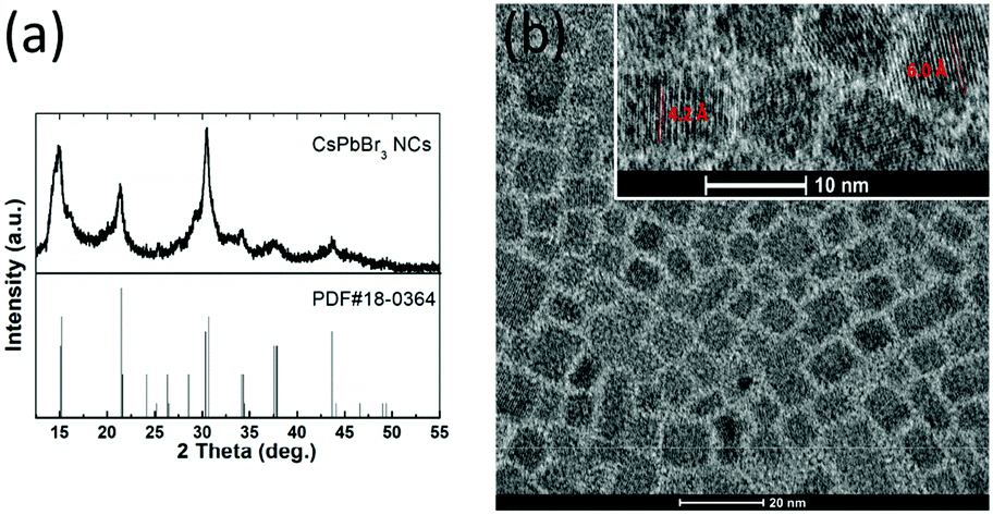 | ||
| Fig. 1 (a) XRD patterns of synthesized CsPbBr3 NCs and a standard monoclinic sample, (b) low- and high-resolution TEM images of CsPbBr3 NCs. | ||
UV-Vis absorption and PL emission spectra of the CsPbBr3 NC thin film are shown in Fig. 2(a). The perovskite thin film produces a narrow emission spectrum under 365 nm excitation with an emission peak at 504 nm; the FWHM of the PL peak is only 22 nm. The narrow emission spectrum indicates superior color purity for display applications. The UV-Vis absorption band at >504 nm suggests the presence of large particles or unreacted precursors.39 Time-resolved PL was performed on the perovskite film to investigate exciton recombination dynamics, as shown in Fig. 2(b). The decay curve is fitted to bi-exponential decay functions, and the fitting results indicate a short-lived PL lifetime (τ1) of 5.1 ns (68.2%), a long-lived PL lifetime (τ2) of 18.3 ns (31.8%), and an average PL lifetime (τave) of 9.3 ns, which indicate a relatively high ratio of radiative to non-radiative transitions.40
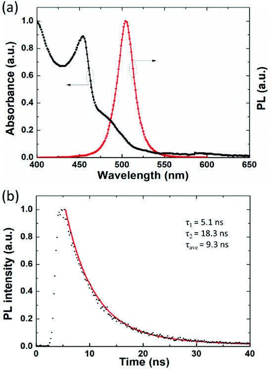 | ||
| Fig. 2 (a) UV-Vis absorption and PL (365 nm excitation) spectra of the CsPbBr3 NC film, (b) PL decay and fitting curve of the CsPbBr3 NC film. | ||
We subsequently employed CsPbBr3 NCs as the emitting material in inverted devices, as described in the Experimental section. Fig. 3 shows the structure of the device and the corresponding energy levels of the materials in the inverted CsPbBr3 NC LEDs.22,31,41,42
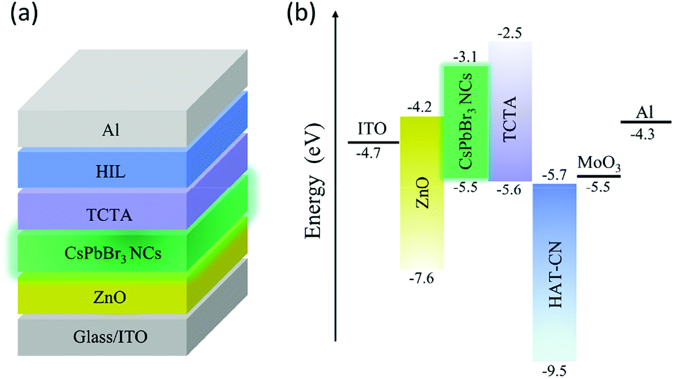 | ||
| Fig. 3 (a) Device structure of the inverted CsPbBr3 NC LEDs, (b) schematic energy level diagram of materials used in the device. | ||
TCTA, with a highest occupied molecular orbital (HOMO) level of −5.6 eV, was selected as the HTL to match the VB edge of the CsPbBr3 NC film. The effectiveness of HAT-CN as a HIL or a dopant in the HTL has been reported previously.33,34 The six carbonitrile units in HAT-CN have a strong electron-withdrawing ability; hence, HAT-CN can be used as electron acceptor (p-doping material), owing to its large electron affinity.43 In most oxides, a particular defect will dominate under atmospheric environment. MoO3 intrinsically behaves as an n-type material because its dominant defect is an oxygen vacancy. As an n-type oxide with wide band gap, MoO3 has also proven effective for hole injection.35 To verify the effectiveness of both HAT-CN and MoO3 for hole injection, inverted CsPbBr3 NC LEDs with no HIL and two types of single HILs were fabricated. Among them, device B and C have single HILs with HAT-CN and MoO3, respectively. The device structures are as follows:
Device A: ITO/ZnO (25 nm)/NCs (30 nm)/TCTA (40 nm)/Al (100 nm).
Device B: ITO/ZnO (25 nm)/NCs (30 nm)/TCTA (40 nm)/HAT-CN (10 nm)/Al (100 nm).
Device C: ITO/ZnO (25 nm)/NCs (30 nm)/TCTA (40 nm)/MoO3 (10 nm)/Al (100 nm).
The EL performances of devices A, B and C are shown in Fig. 4. Firstly, only device C emits light, while devices A (with no HIL) and B (with a HAT-CN HIL) exhibit extremely low currents without any light. Al with a low work function (4.3 eV) was deposited directly on TCTA without HIL in device A; hence, the interface barrier is prohibitively high for effective hole injection. In device B, the high interface barrier between Al and HAT-CN causes electron accumulation in HAT-CN and makes electron extraction from TCTA difficult. In addition, atomic force microscopy (AFM) of the HAT-CN film (Fig. 5(a)) reveals that it has a relatively rough surface with a root-mean-square (RMS) value of 5.25 nm, which may be caused by the complex hexagonal arrangement of the crystalline structure of HAT-CN.34,44 The rough surface renders a smaller contact area between HAT-CN and the Al electrode, which is unfavorable to hole injection. It also has been reported that connecting HAT-CN separately as a single HIL to various HTLs (the HOMO level from −6.22 eV to −5.4 eV) does not provide effective hole injection.45
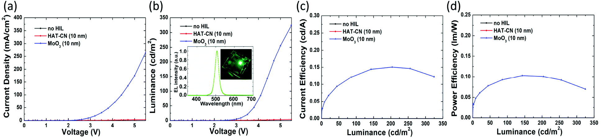 | ||
| Fig. 4 (a) Current density–voltage, (b) luminance–voltage, (c) current efficiency–luminance, and (d) power efficiency–luminance of the inverted CsPbBr3 NC LEDs with no HIL and different single HILs. Inset: device C operating at a voltage of 5 V and its EL spectrum. | ||
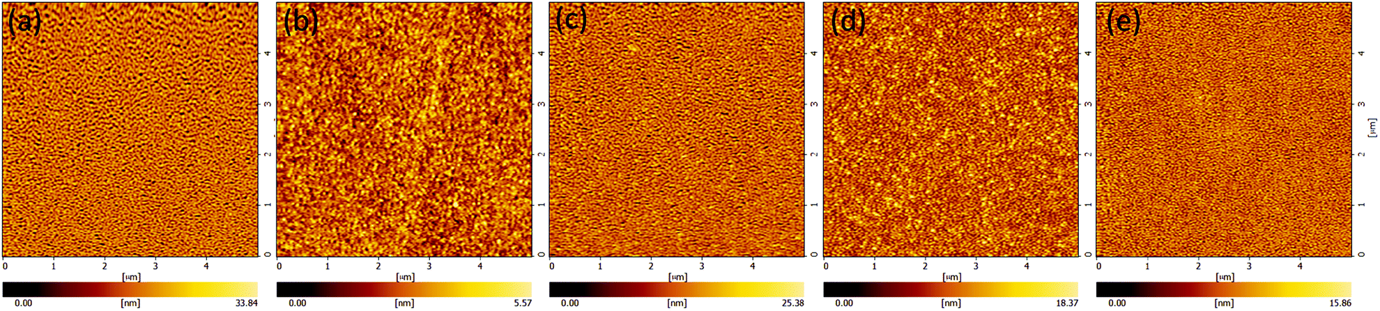 | ||
| Fig. 5 AFM images of (a) HAT-CN (10 nm), (b) MoO3 (10 nm), (c) HAT-CN (7.5 nm)/MoO3 (2.5 nm), (d) HAT-CN (5 nm)/MoO3 (5 nm), and (e) HAT-CN (2.5 nm)/MoO3 (7.5 nm) on TCTA (40 nm) film. | ||
In contrast, the EL performance of device C confirms that the introduction of MoO3 is necessary to the device. As presented in the inset of Fig. 4(b), the emission peak of device C appears at 506 nm with a narrow FWHM of approximately 23 nm. Compared to the PL spectrum of the CsPbBr3 NC film, the EL peak exhibited a 2 nm red-shift, which may be attributed to the electric-field-induced Stark effect.46 The turn-on voltage (defined as the voltage at a luminance of 1 cd m−2), maximum CE, and maximum PE of the device C with a single MoO3 HIL are 2.6 V, 0.15 cd A−1, and 0.1 lm W−1, respectively. A series of interface states generated between MoO3 and the Al anode as a consequence of MoO3 film insertion; these are attributed to a reduced Mo5+ phase by hole injection from Al.47 They are very close to the Fermi level of Al and overlap each other, increasing the work function of Al, and eventually facilitating hole injection and transport. Furthermore, as can be observed in Fig. 5(b), MoO3 (10 nm) is very uniform (RMS = 0.86 nm) over the whole area, contributing to efficient hole injection.
Compared to the electron mobility of ZnO (1.8 × 10⁻³ cm2 V−1 s−1), the hole mobility of TCTA (3 × 10⁻⁴ cm2 V−1 s−1) is much lower,31,48 resulting in unbalanced charge carriers in the EML. To further enhance hole injection to the EML, we tried to insert a thin film of HAT-CN between MoO3 and the HTL. As mentioned, the strong electron-withdrawing properties of HAT-CN may allow it to extract electrons from the hole transport materials with suitable HOMO levels when in contact with them, generating numerous holes to improve hole injection and transport. Three dual HIL devices with different thickness ratios of HAT-CN and MoO3 were fabricated. The HIL thickness was maintained for consistent cavity length; the device structures are as follows:
Device D: ITO/ZnO (25 nm)/NCs (30 nm)/TCTA (40 nm)/HAT-CN (7.5 nm)/MoO3 (2.5 nm)/Al (100 nm).
Device E: ITO/ZnO (25 nm)/NCs (30 nm)/TCTA (40 nm)/HAT-CN (5 nm)/MoO3 (5 nm)/Al (100 nm).
Device F: ITO/ZnO (25 nm)/NCs (30 nm)/TCTA (40 nm)/HAT-CN (2.5 nm)/MoO3 (7.5 nm)/Al (100 nm).
The EL performances of devices D, E and F are shown in Fig. 6. Devices E and F are illuminated, while device D, containing the thinnest MoO3 film, exhibits almost no current under the driving voltages. As mentioned earlier, when used as the HIL, MoO3 can increase the work function of Al and thus decrease the hole injection barrier. It is noteworthy that increasing the work function of Al has a close positive correlation to the thickness of MoO3 in the range of several nanometers, and then the work function plateaus with thicker MoO3 films.47 The MoO3 film in device D is only 2.5 nm; this results in difficulty in hole injection. In another word, the MoO3 film is too thin to increase the work function of Al sufficiently, so that the barrier for hole injection is still too high. Meanwhile, as illustrated in Fig. 5(c), RMS value of the dual HIL surface of device D is 3.74 nm, which may negatively affect hole injection.
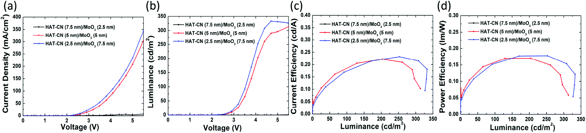 | ||
| Fig. 6 (a) Current density–voltage, (b) luminance–voltage, (c) current efficiency–luminance, and (d) power efficiency–luminance of the inverted CsPbBr3 NC LEDs with different thicknesses of HAT-CN and MoO3. | ||
Table S2† summarizes the performances of CsPbBr3 NC LEDs with different HILs. It is clear that the EL performances are enhanced for devices with dual HILs compared to those with a single HIL. Devices E and F have higher current densities than device C under the same driving voltage, and their turn-on voltages are 2.3 V, lower than that of device C (2.6 V). At 300 cd m−2, the driving voltages for devices C, E, and F are 5.3, 5.2, and 4.4 V, respectively. The maximum CE and PE of device F are 0.23 cd A−1 and 0.18 lm/W respectively, which are 1.5- and 1.8-fold higher than those of device C, which contains a single MoO3 HIL. Meanwhile, device E and F show a current density of 207.6 and 233.2 mA cm−2, over 1.18- and 1.34-fold higher than that of device C (174.6 mA cm−2) at the driving voltage of 5 V. From Fig. 5(d) and (e), device E and F have a rougher surface of the HIL but show higher current densities than those of device C. In view of this, we believe that the extra hole injection paths in device C are not enough to make up for the lack of HAT-CN. In addition, devices with a structure of ITO/TCTA/HIL/Al were fabricated to ensure the hole injection enhancement of the dual-HIL device. As shown in Fig. 7, the current density of the device with a HAT-CN/MoO3 HIL is higher than that of the device with a MoO3 HIL. The results demonstrate that the introduction of a thin HAT-CN film can effectively promote hole injection.
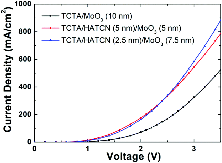 | ||
| Fig. 7 Current density–voltage characteristics of the hole-only devices with different HILs, where the device structure is ITO/TCTA (40 nm)/HIL/Al (100 nm). | ||
In general, the hole injection efficiency depends on the barrier height and the hole mobility of the hole transport layer. In our dual HIL devices, MoO3 and HAT-CN play important and distinct roles for hole injection. MoO3 increases the work function of Al effectively, thus decreasing the barrier for hole injection at the interface; it also provides a smooth surface for adequate contact area with Al, resulting in more hole injection paths. HAT-CN, with high electron mobility and a large electron affinity,41,49 allows the facile transfer of electrons from the HOMO level of TCTA to the LUMO level of it. This electron loss is equivalent to hole injection, as illustrated in Fig. 8. The process, which occurs at the interface between HAT-CN and TCTA, is similar to what occurs at the interface between NPB or TAPC and HAT-CN.43,50–52 Meanwhile, the high electron mobility of HAT-CN makes electron transport quick from HAT-CN to Al/MoO3. The hole mobility would be enhanced due to the coulombic interaction at the charge recombination interface and the high electron mobility of HAT-CN.49 Finally, the introduction of the dual HIL greatly enhances the hole injection efficiency and the EL performances.
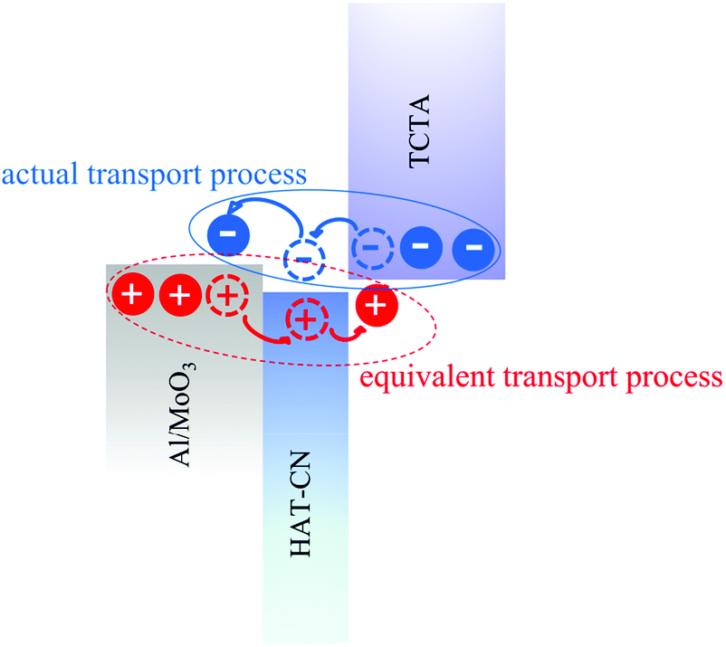 | ||
| Fig. 8 Diagram of charges generation at the interface between TCTA and MoO3. | ||
4. Conclusions
In summary, CsPbBr3 NCs with a narrow particle size distribution and a narrow emission spectrum were synthesized by a LARP method. In inverted CsPbBr3 NC LEDs, a dual HIL comprising HAT-CN and MoO3 is introduced to enhance hole injection. As the dual HIL, HAT-CN generates numerous free holes at the interface while MoO3 increases the work function of the Al anode to improve hole injection. Finally, compared to the single HIL device, the CE and PE were improved 1.5- and 1.8-fold, respectively, with HAT-CN (2.5 nm)/MoO3 (7.5 nm) as a dual HIL. These results demonstrate that a dual HAT-CN/MoO3 HIL, connected to TCTA, can effectively promote hole injection, and has potential for application with many other devices.Conflicts of interest
There are no conflicts to declare.Acknowledgements
This work was supported by the National Key R&D Program of China (2017YFB1002900) and the National Natural Science Foundation of China (61675127, 61975117).References
- J. Pan, L. N. Quan, Y. B. Zhao, W. Peng, B. Murali, S. P. Sarmah, M. J. Yuan, L. Sinatra, N. M. Alyami, J. K. Liu, E. Yassitepe, Z. Y. Yang, O. Voznyy, R. Comin, M. N. Hedhili, O. F. Mohammed, Z. H. Lu, D. H. Kim, E. H. Sargent and O. M. Bakr, Adv. Mater., 2016, 28, 8718–8725 CrossRef CAS PubMed
.
- J. H. Li, L. M. Xu, T. Wang, J. Z. Song, J. W. Chen, J. Xue, Y. H. Dong, B. Cai, Q. S. Shan, B. N. Han and H. B. Zeng, Adv. Mater., 2017, 29, 1603885 CrossRef PubMed
- W. Cai, Z. Chen, D. Chen, S. Su, Q. Xu, H.-L. Yip and Y. Cao, RSC Adv., 2019, 9, 27684–27691 RSC
- K. Wei, Z. J. Xu, R. Z. Chen, X. Zheng, X. G. Cheng and T. Jiang, Opt. Lett., 2016, 41, 3821–3824 CrossRef CAS PubMed
- Y. Wang, X. M. Li, J. Z. Song, L. Xiao, H. B. Zeng and H. D. Sun, Adv. Mater., 2015, 27, 7101–7108 CrossRef CAS PubMed
- C. Y. Huang, C. Zou, C. Y. Mao, K. L. Corp, Y. C. Yao, Y. J. Lee, C. W. Schlenker, A. K. Y. Jen and L. Y. Lin, ACS Photonics, 2017, 4, 2281–2289 CrossRef CAS
- M. G. Gong, R. Sakidja, R. Goul, D. Ewing, M. Casper, A. Stramel, A. Elliot and J. Z. Wu, ACS Nano, 2019, 13, 1772–1783 CrossRef CAS PubMed
- P. Ramasamy, D. H. Lim, B. Kim, S. H. Lee, M. S. Lee and J. S. Lee, Chem. Commun., 2016, 52, 2067–2070 RSC
- X. M. Li, D. J. Yu, F. Cao, Y. Gu, Y. Wei, Y. Wu, J. Z. Song and H. B. Zeng, Adv. Funct. Mater., 2016, 26, 5903–5912 CrossRef CAS
- L. M. Wheeler, E. M. Sanehira, A. R. Marshall, P. Schulz, M. Suri, N. C. Anderson, J. A. Christians, D. Nordlund, D. Sokaras, T. Kroll, S. P. Harvey, J. J. Berry, L. Y. Lin and J. M. Luther, J. Am. Chem. Soc., 2018, 140, 10504–10513 CrossRef CAS PubMed
- A. Swarnkar, A. R. Marshall, E. M. Sanehira, B. D. Chernomordik, D. T. Moore, J. A. Christians, T. Chakrabarti and J. M. Luther, Science, 2016, 354, 92–95 CrossRef CAS PubMed
- S. Panigrahi, S. Jana, T. Calmeiro, D. Nunes, R. Martins and E. Fortunato, ACS Nano, 2017, 11, 10214–10221 CrossRef CAS PubMed
- Y. T. Dong, T. Qiao, D. Kim, D. Parobek, D. Rossi and D. H. Son, Nano Lett., 2018, 18, 3716–3722 CrossRef CAS PubMed
- A. Swarnkar, R. Chulliyil, V. K. Ravi, M. Irfanullah, A. Chowdhury and A. Nag, Angew. Chem., Int. Ed., 2015, 54, 15424–15428 CrossRef CAS PubMed
- X. M. Li, Y. Wu, S. L. Zhang, B. Cai, Y. Gu, J. Z. Song and H. B. Zeng, Adv. Funct. Mater., 2016, 26, 2435–2445 CrossRef CAS
- X. Zhang, C. Sun, Y. Zhang, H. Wu, C. Ji, Y. Chuai, P. Wang, S. Wen, C. Zhang and W. W. Yu, Chem. Phys. Lett., 2016, 7, 4602–4610 CrossRef CAS PubMed
- J. Yang, B. D. Siempelkamp, D. Liu and T. L. Kelly, ACS Nano, 2015, 9, 1955–1963 CrossRef CAS PubMed
- B. Conings, J. Drijkoningen, N. Gauquelin, A. Babayigit, J. D'Haen, L. D'Olieslaeger, A. Ethirajan, J. Verbeeck, J. Manca and E. Mosconi, Adv. Energy Mater., 2015, 5, 1500477 CrossRef
- L. C. Schmidt, A. Pertegás, S. González-Carrero, O. Malinkiewicz, S. Agouram, G. Minguez Espallargas, H. J. Bolink, R. E. Galian and J. Pérez-Prieto, J. Am. Chem. Soc., 2014, 136, 850–853 CrossRef CAS PubMed
- J. Z. Song, J. H. Li, L. M. Xu, J. H. Li, F. J. Zhang, B. N. Han, Q. S. Shan and H. B. Zeng, Adv. Mater., 2018, 30, 1800764 CrossRef PubMed
- F. Zhang, H. Z. Zhong, C. Chen, X. G. Wu, X. M. Hu, H. L. Huang, J. B. Han, B. S. Zou and Y. P. Dong, ACS Nano, 2015, 9, 4533–4542 CrossRef CAS PubMed
- E. Moyen, H. Jun, H. M. Kim and J. Jang, ACS Appl. Mater. Interfaces, 2018, 10, 42647–42656 CrossRef CAS PubMed
- J. Z. Song, J. H. Li, X. M. Li, L. M. Xu, Y. H. Dong and H. B. Zeng, Adv. Mater., 2015, 27, 7162–7167 CrossRef CAS PubMed
- Q. V. Le, K. Hong, H. W. Jang and S. Y. Kim, Adv. Electron. Mater., 2018, 4, 1800335 CrossRef
- S. Zou, Y. Liu, J. Li, C. Liu, R. Feng, F. Jiang, Y. Li, J. Song, H. Zeng, M. Hong and X. Chen, J. Am. Chem. Soc., 2017, 139, 11443–11450 CrossRef CAS PubMed
- K. Lin, J. Xing, L. N. Quan, F. P. G. de Arquer, X. Gong, J. Lu, L. Xie, W. Zhao, D. Zhang, C. Yan, W. Li, X. Liu, Y. Lu, J. Kirman, E. H. Sargent, Q. Xiong and Z. Wei, Nature, 2018, 562, 245 CrossRef CAS PubMed
- D. D. Yang, X. M. Li, W. H. Zhou, S. L. Zhang, C. F. Meng, Y. Wu, Y. Wang and H. B. Zeng, Adv. Mater., 2019, 31, 8 Search PubMed
- Q. Khan, A. Subramanian, G. Yu, K. Maaz, D. Li, R. U. R. Sagar, K. Chen, W. Lei, B. Shabbir and Y. Zhang, Nanoscale, 2019, 11, 5021–5029 RSC
- S.-Y. Chen, T.-Y. Chu, J.-F. Chen, C.-Y. Su and C. H. Chen, Appl. Phys. Lett., 2006, 89, 053518 CrossRef
- W. Y. Ji, S. H. Liu, H. Zhang, R. Wang, W. F. Xie and H. Z. Zhang, ACS Photonics, 2017, 4, 1271–1278 CrossRef CAS
- L. Qian, Y. Zheng, K. R. Choudhury, D. Bera, F. So, J. G. Xue and P. H. Holloway, Nano Today, 2010, 5, 384–389 CrossRef CAS
- Z. R. R. Tian, J. A. Voigt, J. Liu, B. McKenzie, M. J. McDermott, M. A. Rodriguez, H. Konishi and H. F. Xu, Nat. Mater., 2003, 2, 821–826 CrossRef CAS PubMed
- Y. R. Cho, P.-G. Kang, D. H. Shin, J.-H. Kim, M.-J. Maeng, J. Sakong, J.-A. Hong, Y. Park and M. C. Suh, Appl. Phys. Express, 2015, 9, 012103 CrossRef
- D. Dong, F. Zhu, S. Wu, L. Lian, H. Wang, D. Xu and G. He, Org. Electron., 2019, 68, 22–27 CrossRef CAS
- M. T. Greiner and Z.-H. Lu, NPG Asia Mater., 2013, 5, e55 CrossRef CAS
- S. B. Heo, J. H. Yu, M. Kim, Y. Yi, J. E. Lee, H. K. Kim and S. J. Kang, RSC Adv., 2019, 9, 11996–12000 RSC
- X. Zhang, F. You, S. Liu, B. Mo, Z. Zhang, J. Xiong, P. Cai, X. Xue, J. Zhang and B. Wei, Appl. Phys. Lett., 2017, 110, 043301 CrossRef
- A. Pan, B. He, X. Fan, Z. Liu, J. Urban, A. Alivisatos, L. He and y. Liu, ACS Nano, 2016, 10, 7943–7954 CrossRef CAS PubMed
- J. Lan, L. Luo, M. Wang, F. Li, X. Wu and F. Wang, J. Lumin., 2019, 210, 464–471 CrossRef CAS
- X. Li, Y. Wu, S. Zhang, B. Cai, Y. Gu, J. Song and H. Zeng, Adv. Funct. Mater., 2016, 26, 2584 CrossRef CAS
- K. S. Yook, S. O. Jeon and J. Y. Lee, Thin Solid Films, 2009, 517, 6109–6111 CrossRef CAS
- J. Kwak, W. K. Bae, D. Lee, I. Park, J. Lim, M. Park, H. Cho, H. Woo, D. Y. Yoon and K. Char, Nano Lett., 2012, 12, 2362–2366 CrossRef CAS PubMed
- S. M. Park, Y. H. Kim, Y. Yi, H.-Y. Oh and J. Won Kim, Appl. Phys. Lett., 2010, 97, 176 Search PubMed
- P. Szalay, J. Galán-Mascarós, R. Clérac and K. Dunbar, Synth. Met., 2001, 122, 535–542 CrossRef CAS
- T. Hirose, T. Hamada, T. Tsunoi, E. Aoyama, A. Ishigaki, T. Suzuki, H. Inoue, H. Nakashima, S. Seo and T. Tsutsui, SID Int. Symp. Dig. Tech. Pap., 2016, 47, 1476–1479 CrossRef CAS
- J.-M. Caruge, J. E. Halpert, V. Bulović and M. G. Bawendi, Nano Lett., 2006, 6, 2991–2994 CrossRef CAS PubMed
- Y. Yi, P. E. Jeon, H. Lee, K. Han, H. S. Kim, K. Jeong and S. W. Cho, J. Chem. Phys., 2009, 130, 094704 CrossRef PubMed
- J. W. Kang, S. H. Lee, H. D. Park, W. I. Jeong, K. M. Yoo, Y. S. Park and J. J. Kim, Appl. Phys. Lett., 2007, 90, 223508 CrossRef
- B. B. Diouf, W. S. Jeon, J. S. Park, J. W. Choi, Y. H. Son, D. C. Lim, Y. J. Doh and J. H. Kwon, Synth. Met., 2011, 161, 2087–2091 CrossRef CAS
- Y.-K. Kim, J. Won Kim and Y. Park, Appl. Phys. Lett., 2009, 94, 43 Search PubMed
- J.-H. Kim, J. Seo, D.-G. Kwon, J.-A. Hong, J. Hwang, H. K. Choi, J. Moon, J.-I. Lee, D. Y. Jung and S.-Y. Choi, Carbon, 2014, 79, 623–630 CrossRef CAS
- H. Lee, J. Lee, S. Park, Y. Yi, S. W. Cho, J. W. Kim and S. J. Kang, Carbon, 2014, 71, 268–275 CrossRef CAS
Footnote |
| † Electronic supplementary information (ESI) available. See DOI: 10.1039/d0ra02622k |
| This journal is © The Royal Society of Chemistry 2020 |