
 Open Access Article
 This Open Access Article is licensed under a Creative Commons Attribution-Non Commercial 3.0 Unported Licence
Investigation of the effect of S/In molar ratio on physical properties of sprayed In2S3 thin films
Y. Bchiria,
N. Bouguila *a,
M. Krainia,
R. Souissibc,
C. Vázquez-Vázquezd,
M. A. López-Quintelad and
S. Alayaa
*a,
M. Krainia,
R. Souissibc,
C. Vázquez-Vázquezd,
M. A. López-Quintelad and
S. Alayaa
aLaboratoire de Physique des Matériaux et des Nanomatériaux appliquée à l’Environnement, Faculté des Sciences, Université de Gabès, Cité Erriadh Manara Zrig, 6072, Gabès, Tunisia. E-mail: nour.bouguila@fsg.rnu.tn
bTunis University, Ecole Nationale Supérieure d'ingénieurs de Tunis (ENSIT), Tunisia
cUniversité de Carthage, Laboratoire des Matériaux, Molécules et Applications IPEST, BP 51, La Marsa 2070, Tunis, Tunisia
dLaboratory of Magnetism and Nanotechnology (NANOMAG), Department of Physical Chemistry, Faculty of Chemistry, Universidade de Santiago de Compostela, 15782 Santiago de Compostela, Spain
First published on 10th June 2020
Abstract
Indium sulfide (In2S3) thin films have been synthesized on glass substrates using the spray technique (CSP). The S![[thin space (1/6-em)]](https://www.rsc.org/images/entities/char_2009.gif) :In molar ratio was varied from 1 to 4 in the starting solution. The Raman analysis confirms the formation of the β-In2S3 material and the absence of a secondary phase. The EDS analysis reveals that our layers are pure. The thin film surface is free of cracks, as observed in AFM images. Optical transmission achieved 80% in the visible and near infrared region. The refractive index (n) is affected by the changes in the S/In molar ratio. The optical parameters, single oscillator energy (E0), dispersion energy (Ed) and high frequency dielectric constant (ε∞), are calculated via the Wemple–DiDomenico model. In addition, the photoconductivity kinetics in In2S3 films for S/In = 2 were investigated and analyzed. The I–V characteristics and the photoresponse were also studied.
:In molar ratio was varied from 1 to 4 in the starting solution. The Raman analysis confirms the formation of the β-In2S3 material and the absence of a secondary phase. The EDS analysis reveals that our layers are pure. The thin film surface is free of cracks, as observed in AFM images. Optical transmission achieved 80% in the visible and near infrared region. The refractive index (n) is affected by the changes in the S/In molar ratio. The optical parameters, single oscillator energy (E0), dispersion energy (Ed) and high frequency dielectric constant (ε∞), are calculated via the Wemple–DiDomenico model. In addition, the photoconductivity kinetics in In2S3 films for S/In = 2 were investigated and analyzed. The I–V characteristics and the photoresponse were also studied.
1. Introduction
Most promising sulfide based semiconductor materials have been used as light absorbers in solar cells such as chalcopyrite CuInS2, paramagnetic insulator Fe1−xCoxS2, antimony sulfide Sb2S3 and sulfide indium In2S3. The thermodynamic efficiency of various devices is of wide interest because of the relevance of this parameter for energy conversion.The efficiency of MEH-PPV/H-CuInS2 hybrid solar cells was studied by Yue et al.1 Hierachical CuInS2 was deposited with the induction of histidine by solvothermal method. The authors found that devices based on H-CuInS2 synthesized with smaller size (0.5 HD) displayed higher energy conversion efficiency of 0.59%. The chalcopyrite CuInS2 quantum dots (CuInS2-QDs) with different sizes synthesized by the solvothermal method was used in MEH-PPV–CuInS2/TiO2-NA solar cells.2 The authors obtained a peak efficiency of 1.60% for the 5.4 nm CuInS2-QDs. In addition, this efficiency is comparable to the QDSSCs based on CdS sensitized TiO2-NA.3
Recently, a series of Fe1−xCoxS2 (x = 0–0.5) solid solutions have been synthesized and served as counter electrodes in dye sensitized solar cells (DSSCs).4 The results reveal high power conversion efficiency of 8.36% than those solid solutions materials over Pt of 7.66%. Wu et al.5 studied hybrid TiO2/Sb2S3/P3HT n–i–p solar cells with Sb2S3 layers of different thickness by CBD method. They reported an optimum efficiency of 1.65% with Sb2S3 thickness of 175 nm.
However, the use of cadmium (Cd) in PV devices is undesirable from the viewpoint of environmental safety,6 serious efforts have been made to substitute the CdS by other non-toxic (Cd-free). Indium sulfide (In2S3) is one of the possible candidates to replace CdS a buffer layer. This compound is an n-type semiconductors which belongs to III–VI group. Hetro-juncture such as CIGS/β-In2S3 (ref. 7) achieved a conversion efficiencies of 15.7%. This demonstrates that comparable conversion efficiencies can be obtained respect to commonly used CdS buffer (16%).8 Osman et al.9 observed that there is no difference between both structures of CdS and In2S3, they found also that the efficiency of CIGS solar cells with both layers is comparable. It's 24.14% and 24.28% with In2S3 and CdS respectively.
In2S3 is currently researched as a result of its important properties in relation with the optoelectronic devices.10 β-In2S3 is recognized as a direct band gap semiconductor ranging from 2.0 to 2.75 eV, with a high stability, high optical transmittance (>80%) and controllable electrical properties, modified chemical composition and deposition parameters.11,12 These characteristics of In2S3 films make it a useful material for several applications. In2S3 can be used in light-emitting diode (LED) and lithium-ion batteries.13,14 Due to its absorption in the UV and visible region, In2S3 is considered as photodetector.15 Also, this material can be used for gas sensing and photocatalytic applications owing to its thermal stability, good response and reversibility, low defect density and simple synthesis process.16,17
In2S3 exists in three different crystalline phases α, β and γ which depend on the growth temperature.12,18 β-In2S3 is the most stable phase at room temperature.19,20 It crystallizes in a defect spinel structure with a high degree of tetrahedral and octahedral vacancy sites.21,22
Various techniques were commonly used for preparing In2S3 such as spray pyrolysis,23,24 ultrasonic dispersion,25 physical vapor deposition,26 chemical bath deposition,27 vacuum thermal evaporation,28 etc. Among these methods, the spray pyrolysis technique is of particular interest because it is economical and allows growing large area In2S3 thin films. Furthermore, this technique has been applied to fabricate various type of materials such as ZnO and carbon nanofibres (ECN/TiO2).29,30 Indeed, Ngo et al.30 presented a comparative study between ZnO films deposited by spray coating and ZnO prepared by spin coated. They found that the spray coated sample have higher efficiency (3.76%) than spin coated ZnO (3.11%) due to the increase in FF from 42.38% to 63.14%. So that, to choice of technique is one of important factor in solar cells application.
The physical properties of In2S3 thin films are strongly affected by the deposition parameters.25 Several authors have reported that 340 °C is a good substrate temperature for obtaining best crystallinity.31,32 Thus, various works showed that the S/In ratio has an effect on the structure, the crystallite size33–35 and the optical band gap of the In2S3 films.11,36 Zhang et al.37 have reported that the grain size increases from 32 nm to 34.1 nm with the increase of S/In molar ratio from 1 to 4. Furthermore, the high transmittance is found in the visible and near-infrared range. The energy band gap increases significantly when S/In ratio varies from 1 to 2, then decreases from 2.46 eV to 2.4 eV when S/In increases from 2 to 4. John et al.11 have reported that the use of sulfur-rich solution (S/In = 8/2 instead of S/In = 2/1) decreases the energy band gap from 2.81 to 2.64 eV. The photoluminescence (PL) properties of In2S3 at different S/In ratios have been reported by Elfarrass et al.33 They showed that all the films have two emission bands (green and red band). In addition, Bhira et al.38 have demonstrated that In2S3 thin film has high photoconductivity. Therefore, investigations on the effect of S/In ratio on the In2S3 optical properties are very important, to obtain films that are capable to ensure stable and high efficient devices.
In this work, we report the study of the effect of S/In ratio on the physical properties of In2S3 thin films.
2. Experimental details
In2S3 thin films were produced by spray pyrolysis method using an aqueous solution of indium chloride(III) and thiourea, on glass substrate. The concentration of the precursor InCl3 is 10−2 mol L−1. The S/In ratio in the solution varied in the range 1–4. The substrate temperature was fixed at 340 °C within an accuracy of ±5 °C, in agreement with31,32. Compressed nitrogen was used as a carrier gas at a flow rate of 6 L min−1.The formation of In2S3 results from the following endothermic reaction:
| 2InCl3 + 3SC(NH2)2 + 6H2O → In2S3 + 3CO2 + 6NH4Cl | (1) |
The Raman analysis were conducted using a Jobin-Yvon microRaman spectrometer (T64000) with an argon laser line of 514 nm. The composition of films was done by energy dispersive spectroscopy (EDS). The surface morphology was performed by atomic force microscopy using an XE-100 instrument (Park Systems Corporation). Photoluminescence (PL) measurements were performed at room temperature using laser excitation wavelength of 655 nm. Transmittance spectra measurements have been done using a Shimadzu UV 3101 PC spectrophotometer in the wavelength range from 350 to 1900 nm. The I–V characteristics measured in dark and under illumination were performed using a (HP4140B) source/pico-ammeter. Moreover, the photoresponse of In2S3 thin films was investigated by illuminating the film with a neon light source. The resistance of the sample is measured by using a (HP4140B) Keithley Digital multimeter, interfaced to a computer for data acquisition.
3. Results and discussion
3.1. Structural characterization
The quality of sprayed films was characterized by Raman spectroscopy. It's a powerful technique which allows to determine the phase and the structure of films. Besides, this technique provides the information about the vibration mode in the crystalline phase. The Raman spectra for our films are presented in Fig. 1, which were recorded in the energy region between 100 and 500 cm−1. All the spectra reveal broad bands at 135, 310 and 367 cm−1 with low intensity, showing nanocrystalline nature of the layers. These present bands seem to be typical relative to cubic structural (β-In2S3).39,40 The peak at 135 cm−1 can be assigned to the Eg mode, and the peaks at 310, 367 cm−1 to the A1g mode.40–42 The band appeared at 310 cm−1 is related to the symmetric stretching vibrating mode of InS4 tetrahedral.43 Furthermore, the shift in the position of the bands with molar ratio S/In could be due to the presence of strain developed in the films. The shift is in order of 2 cm−1. This induces the deviation in the interplanar spacing in crystal lattice. The change of S/In ratio does not affect the structure of the layers. In addition, we noticed the absence of secondary phases in the all layers. This finding proved the results obtained by XRD analysis.44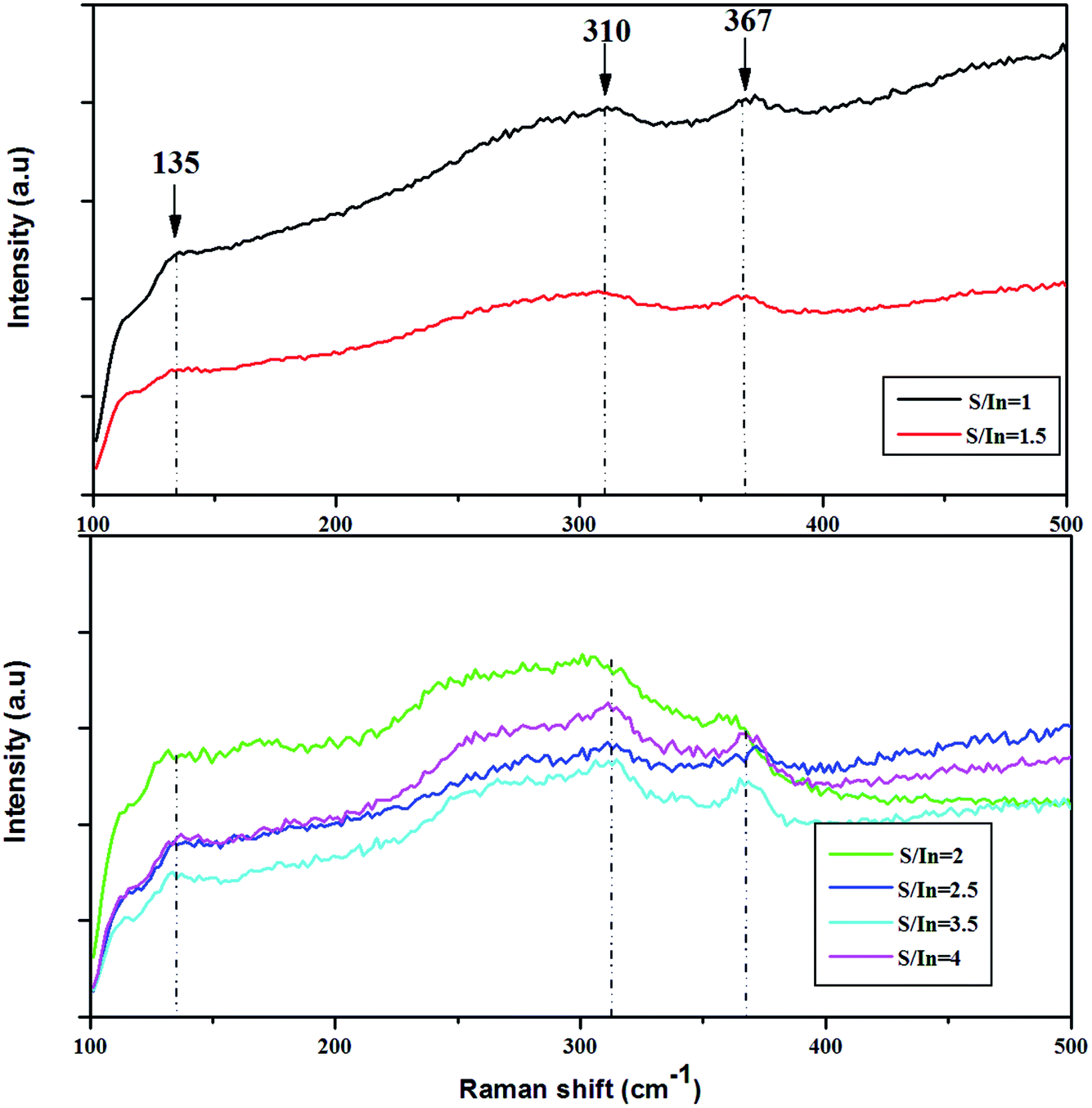 | ||
| Fig. 1 Raman spectra of In2S3 thin films for different S/In molar ratios. | ||
3.2. EDS analysis
The compositional analysis of In2S3 thin films at different S/In molar ratios was carried out employing EDS as shown in Fig. 2a and Table 3. The EDS spectrum confirms the presence of In and S elements in the films, their atomic percentages are given in Table 1. It can be seen that when the S/In increases in the solution, the S/In in the films increases and varies from 0.98 to 1.29. The Cl peak arises from the InCl3 precursor. Also, we notice the presence of various elements such as Si, O, Na and Mg which are provided from glass substrates (see Fig. 2b).45 Therefore, the EDS analysis confirms the purity of deposited In2S3 thin films.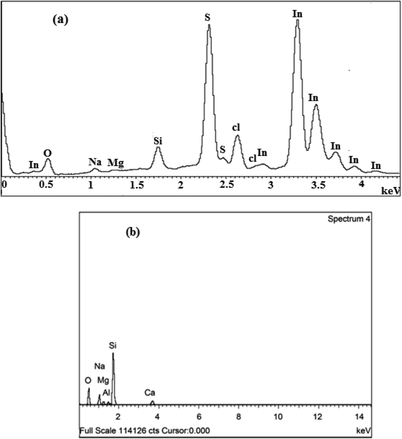 | ||
| Fig. 2 (a) EDS spectra of thin films at different S/In molar ratios. (b) EDX spectrum of glass substrate.45 | ||
| S/In | S (at%) | In (at%) | S/In |
|---|---|---|---|
| 1 | 24.60 | 25.01 | 0.98 |
| 1.5 | 52.18 | 42.34 | 1.23 |
| 2 | 41.93 | 33.51 | 1.24 |
| 2.5 | 46.92 | 36.76 | 1.27 |
| 3.5 | 41.02 | 32.08 | 1.28 |
| 4 | 41.02 | 32.08 | 1.28 |
3.3. Morphological characterization
Fig. 3a shows 2D and 3D NC-AFM images (2 μm × 2 μm) of In2S3 films for S/In ratios equal to 1, 2 and 4. As observed from the AFM images, the surface morphology of the films is sensitive to the S/In molar ratio. Indeed, it can be seen that the films are formed by grains separated by depressions. Owing to the coalescence phenomenon, it appears that the grain size along the surface of the film increases with S/In ratio. Furthermore, we can note also that the films show spherical grains, indicating the polycrystalline nature of these films. This finding agrees with the XRD results. The root mean square roughness (RMS) values decrease from 20 to 6 nm with increasing molar ratio (Table 2). This behavior can be attributed to the increase of crystallite size, and the surface morphology becomes uniform and more compact.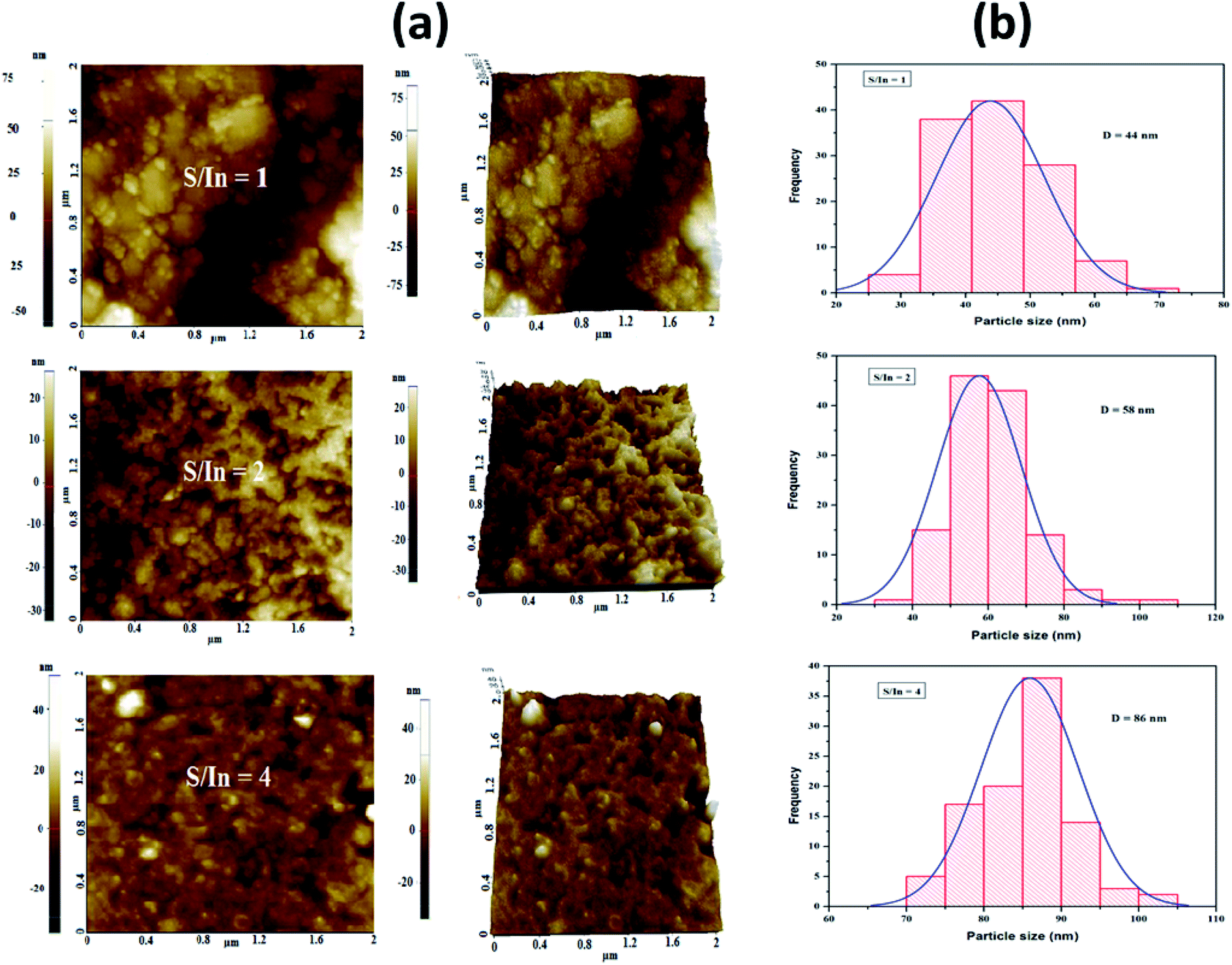 | ||
| Fig. 3 (a) 2D and 3D NC-AFM images of thin films for S/In molar ratios equal to 1, 2 and 4. (b) Grain size distribution histogram of thin films for S/In molar ratios equal to 1, 2 and 4. | ||
| S/In | 1 | 1.5 | 2 | 2.5 | 3.5 | 4 |
| RMS (nm) | 20 | 15 | 11 | 9 | 8 | 6 |
In order to evaluate the average grain size, a statistical count of grain size was performed on the AFM images using Image-J software. Grain size distribution histograms for the different films are shown in Fig. 3b. The average grain size of samples is found to lie in the nanometer range (44–86 nm).
3.4. Optical characterization
Room temperature photoluminescence spectra of In2S3 at different S/In molar ratios are exhibited in Fig. 4. PL spectra reveal a peak at 1.46 eV, 1.52 eV, 2.32 eV and 2.55 eV.
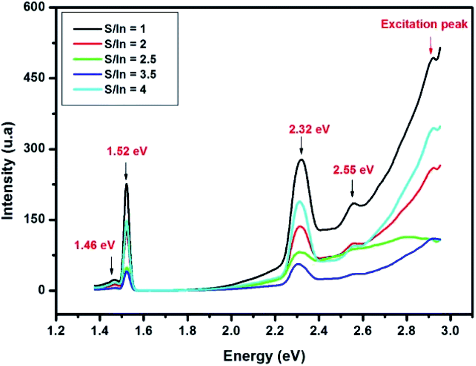 | ||
| Fig. 4 Photoluminescence spectra of In2S3 thin films for different S/In molar ratios. | ||
The red emission at 1.45 is due to S and In vacancies in the host lattice.46 The emission at 1.52 eV and green emission (at 2.32 eV and 2.55 eV) are attributed to transitions from the excited states of the sulfur vacancy (Vs) to the In vacancy (VIn) level.46–48 Mathew et al.22 reported a green emission from In2S3 which was attributed to the donor level formed by indium interstitials. The PL emission intensity is found stranger for sample at S/In = 1 than other samples, which proved the presence of higher defect concentration.49 Thus, the emission intensity decreased indicated the reduction of defects in films. The low emission intensity is obtained for sample at S/In = 3,5, which the crystallinity is the best one. The same result was reported by Ajili et al.50
In addition, the last peak at 2.55 eV is relative to the Eg values estimated from Tauc formula in earlier work by Bouguila et al.44
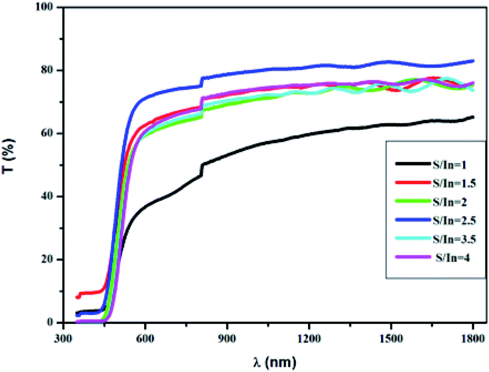 | ||
| Fig. 5 Transmittance spectra with different S/In molar ratios. | ||
| n = (N + (N2 − n20n21)1/2)1/2 | (2) |
 | (3) |
The values of n are reported in Table 3. It can be observed that this value is minimum at S/In = 2.5, beyond this value it increases slightly. This is related to the variation in packing density of the films.54
| S/In | n | B | C (μm2) | β (eV) |
|---|---|---|---|---|
| 1 | 2.40 | 3.14 | −1.0 | 0.16 |
| 1.5 | 2.06 | 2.68 | −0.3 | 0.29 |
| 2 | 2.10 | 2.73 | −0.3 | 0.26 |
| 2.5 | 1.87 | 2.79 | −0.4 | 0.27 |
| 3.5 | 2.11 | 2.81 | −0.2 | 0.31 |
| 4 | 2.03 | 2.84 | −0.4 | 0.26 |
Fresnel equation55 was used to evaluate the refractive index n(λ) of the films as given by:
 | (4) |
Fig. 6 displays the dispersion of n for different molar ratios. In the high absorption region, the refractive index increases strongly. The sharp onset of n at the absorption edge is attributed to Van Hove singularity in the joint density state in the excitation of transition between two bands.56 Thus, it follows the normal dispersion in the medium and weak absorption regions. This latter phenomenon is ascribed to both light scattering effect and absorbance decrease. From Fig. 6, it can be noticed that n varies from 2.4 to 2.75 with S/In ratio. The higher values of n make In2S3 thin films suitable for use in optoelectronic devices. Indeed, thin films are used for optical containment in waveguides, lasers and light-emitting diodes. The good value of n depends on the active layer used.
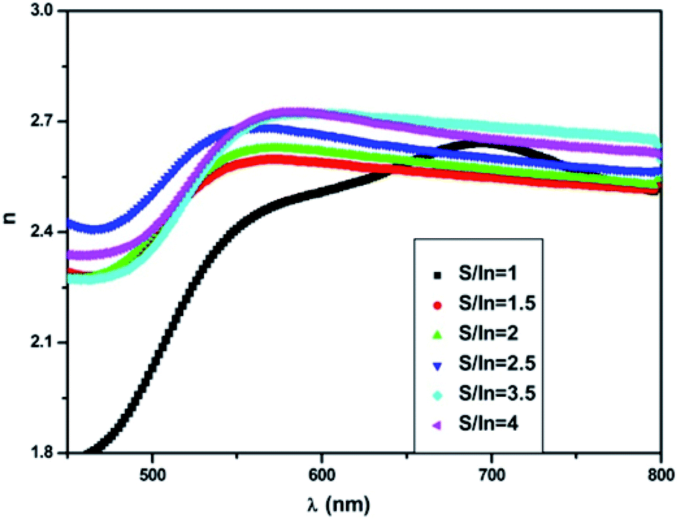 | ||
| Fig. 6 Spectral distribution of n(λ) for different S/In molar ratios. | ||
Thus, the increase of n indicates the better crystallinity of the films. Indeed, the material with amorphous nature has a low refractive index when compared to the polycrystalline one.57
The variation of n along the Cauchy distribution is given by:58
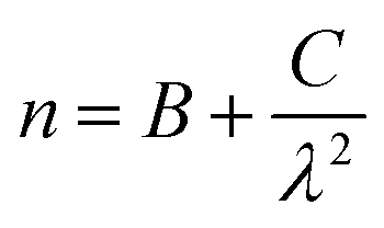 | (5) |
Table 3 represents the values of these constants, which are evaluated from the fitting of n(λ).
The dispersion energy was also calculated using the single oscillator model as described by Wemple and DiDomenico:59
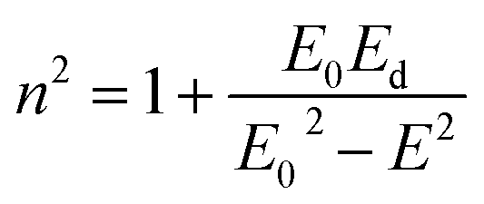 | (6) |
Fig. 7 represents the linear variation of (n2 − 1)−1 versus (hν)2 for these films. This permits us to determine both E0 and Ed from the slope (EdE0)−1 and (E0/Ed) from the intercept at the origin for each straight line.
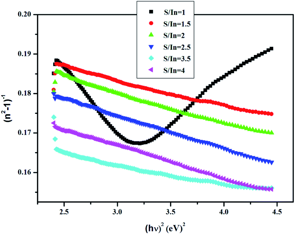 | ||
| Fig. 7 Plot of (n2 − 1)−1 versus (hν)2. | ||
The results are listed in Table 4.
| S/In | 1 | 1.5 | 2 | 2.5 | 3.5 | 4 |
| E0 (eV) | 3.8 | 5.6 | 5.1 | 4.9 | 5.4 | 4.8 |
| Ed (eV) | 15.5 | 27.8 | 25.3 | 25.5 | 30 | 25 |
| EWDDg (eV) | 1.9 | 2.8 | 2.5 | 2.4 | 2.7 | 2.4 |
| ε∞ | 9.6 | 7.5 | 7.8 | 7.4 | 8 | 7.9 |
| ωp (rad s−1) | 14 | 8 | 9 | 10 | 8 | 10 |
| N/m* (m−3) | 6 | 1.5 | 2 | 2 | 1.5 | 2.4 |
The highest dispersion energy value is obtained at S/In = 3.5, indicating that this film has a more ordered microstructure compared to the other films. The microstructure of In2S3 thin films varied with S/In ratio. Indeed, the influence of S/In molar ratio on microstructure is related with the nucleation and grows of In2S3 crystal.60 Furthermore, sulfure deficiency or sulfur excess would involve the presence of impurities that can affect or destroy the microstructure.61
It can also be seen that the values of E0 vary from 3.8 to 5.6 eV and oscillation energy describes the expressions E0 ≈ 1.5Eg at S/In = 1 and E0 ≈ 2Eg for S/In > 1. We can thus conclude that the Wemple–DiDomenico model describes well the behavior of these films.62,63 The lower value of ratio E0 is obtained at S/In = 1, this could be attributed to the higher rate of diffusion of atoms in this film.64 Furthermore, the change in the values of E0 and Ed reveals that the molar ratio S/In is a suitable parameter for the change of refractive index and oscillator parameters. Thus, Tanaka63 proposed the first approximate value of the optical band gap EWDDg from the Wemple–DiDomenico model using the expression (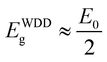 ). The EWDDg values are given in Table 4. The small difference between the two methods is ascribed to the calculations in two different regions. Indeed, in the case of Tauc method, the value of Eg is calculated in the absorption region of the spectrum, while in the Wemple–DiDomenico model the value of EWDDg is acquired in the transparent region of the spectrum.
The following empirical relation for Ed is established in crystals containing a single anion species:65
| Ed = βNeZaNc | (7) |
 | (8) |
 | (9) |
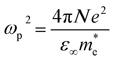
The free carrier concentration-to-effective mass ratio can be obtained from the relation:
 | (10) |
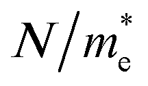 denote respectively the relaxation time, electronic charge, plasma frequency and ratio of carrier concentration to the effective mass.
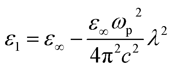
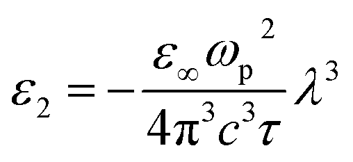
Fig. 8a and b, show that the behavior of ε1 is similar to the refractive index (n). This is due to the smaller value of k compared to n. However, the behaviors of ε2 and α are the same, because ε2 depends on the k values which are correlated to the variation of absorption coefficient (α). We observed high value of ε1 at low wavelengths; this is due to the presence of space charge polarization at the grain boundaries, which generates a potential barrier. Thus, a charge accumulation at the grain boundary occurred, which leads to highest value of ε1.68 However, the real part decreases with the increase of wavelength. This trend is due to the reduction of space charge polarization effect.
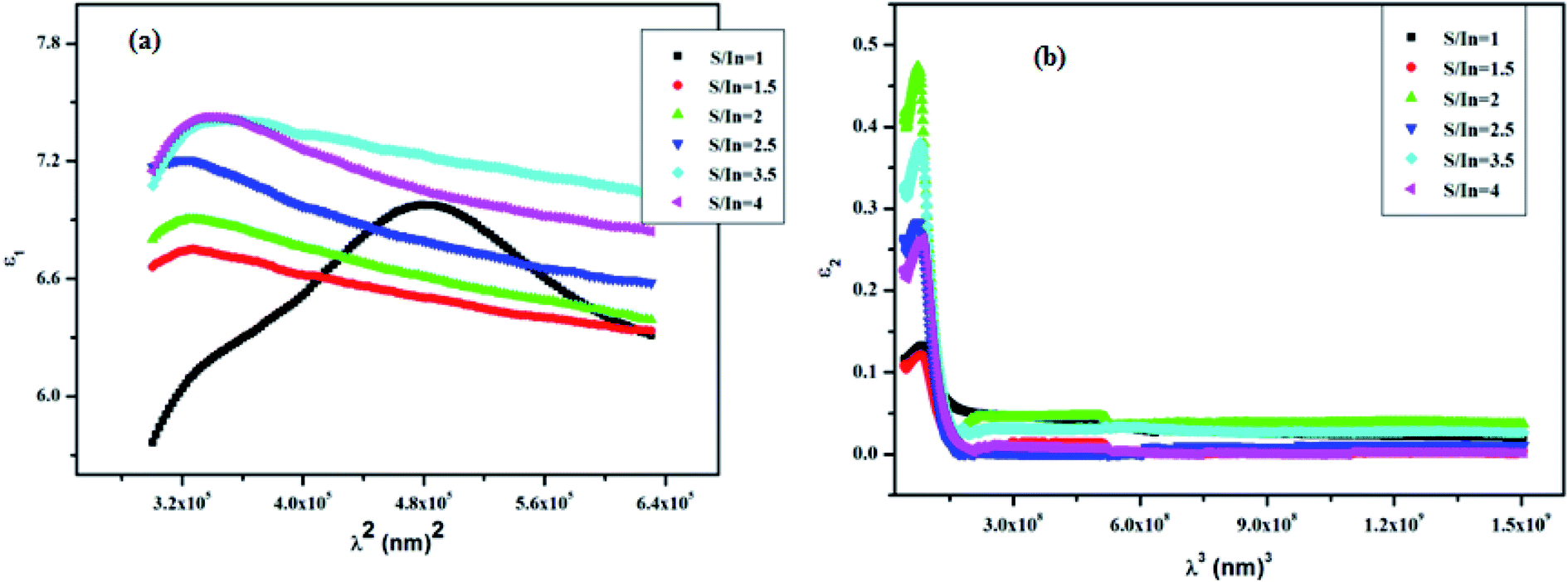 | ||
| Fig. 8 (a) Plot of ε1 versus λ2 and (b) ε2 versus λ3. | ||
From the intercepts and slopes of the ε1 plots as a function of λ2 (see Fig. 8a), the values of ε∞ and N/m* for the films are estimated and reported in Table 4.
The increase in refractive index induces a rise in the electromagnetic radiation absorption which in turn increases the frequency. In addition, the value of n becomes high when the radiation frequency corresponds to the electron characteristic frequency. The physical interpretation of the variation of plasma frequency can be ascribed to the variation of the concentration of the charged carriers in In2S3 thin films. Hence, the high value of ωp at S/In = 1 might be due to the higher concentration of the charged carriers in this film. This finding confirms the results of optical band gap value at S/In = 1. As can be seen, all N/m* values are of the order of 1049 m−3. Bouguila et al.69 reported comparable values for In2S3 thin films for different thicknesses. The higher value obtained at S/In = 1, could be explained by higher defect states in the film.70 Besides, Nicholas et al.71 reported that the low value of effective mass leads to high carrier mobility. Thus, it is clear from Table 2 that the values of N/m* are affected by the S/In molar ratio. So, we can say that ε∞ and N/m* are assigned to the internal microstructure.72
4. Photoresponse
Due to absorption in the UV and visible region, In2S3 is considered here as photodetector. To study the photoresponse of the In2S3 film (S/In = 2), two rectangular gold electrodes 3 mm long and 3 mm apart were deposited on the film using thermal evaporation technique under high vacuum. The samples obtained have the shape of a parallelepiped, the dimensions of the glass substrate are (L = 10 mm, l = 5 mm, w = 2 mm) and the In2S3 film thickness is around 2 μm (Fig. 9).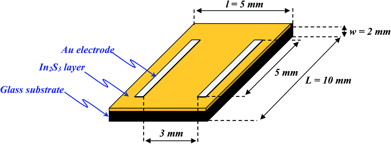 | ||
| Fig. 9 Shape of In2S3 photodetector. | ||
I–V characteristics measured in dark and under illumination by neon lamp with a bias voltage ranging from −10 to 10 volts are shown in Fig. 10a. The linear I–V curves from the sample confirm the ohmic nature of Au/In2S3 contacts. This ohmic contact with Au electrodes enables excellent photo-response behaviors. Furthermore, the formation of ohmic contacts between semiconductors and metals serving as electrodes is an important requirement for photodetector device. Indeed, this contact is required to inject the maximum current density across the contact.73
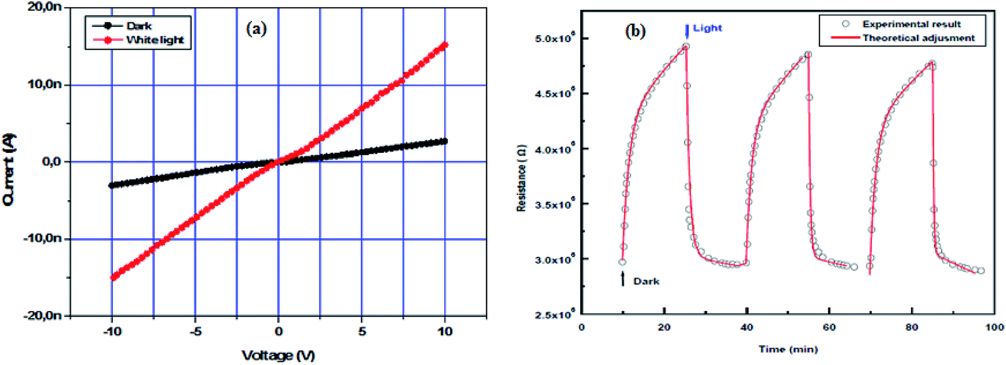 | ||
| Fig. 10 (a) I–V characteristics of In2S3 thin film in dark and under illumination, (b) adjustment of In2S3 thin film photoresponse with two exponentials evolutions. | ||
The resistance evolution was measured, while the sample was illuminated by reversible switching (ON/OFF) cycles of the neon lamp. The light was ON for 15 min and OFF for 15 min for all cycles. Fig. 10b shows that the resistance of In2S3 film increases in dark until reaching its equilibrium value and decreases quickly to the baseline value in light. We also observe that repetitive cycles profile reveals the ability of the material to produce the same response, by exhibiting an acceptable reproducibility and reversibility of the response. This evolution suggests that more photons with higher energy are involved in the photon-induced charge-transfer process. This behavior is suitable given the fact that typical absorption is located for wavelength < 500 nm, as shown in Fig. 5. Likewise, the optical excitation allows the generation of electron–hole pairs. The fact that the transit time of the holes is much greater than that of the electrons; a single hole can cause the circulation of several electrons in order to ensure the electrical neutrality of the material, which enhances photocurrent response.74
The increase of photocurrent is traduced by the decrease of the resistance. In this context, we have adjusted in Fig. 10b, the resistance curves versus time with a bi-exponential equations that have two evolution components in both decaying and rising progress:74
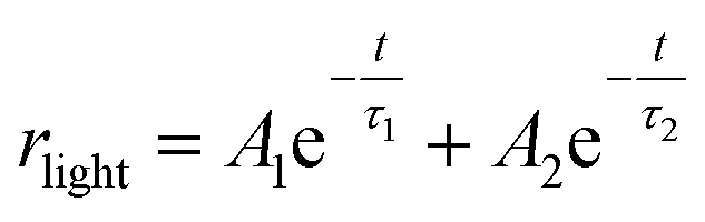 | (11) |
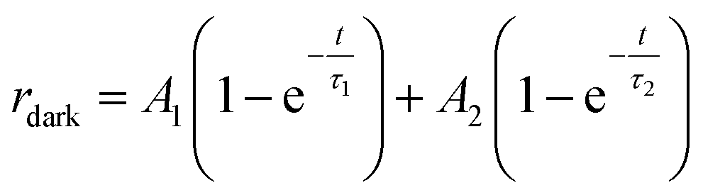 | (12) |
The determination of the constants A1, A2, τ1 and τ2 is not obvious given the nonlinearity of the eqn (11) and (12). As a result, we divide each film response into two parts:
-the first part is dominated by the fast kinetic (τ1) and corresponds to a significant variation of the resistance.
-the second part is dominated by a slow kinetic (τ2) and results in a weak variation of the resistance.
We have adjusted the last points of the second domain (t ≫ τ1) by the function A2e−t/τ2 and we have deduced A2 and τ2 values using the least squares method. Then, the quantity A2e−t/τ2 is subtracted from the experimental points of the first domain (0 < t < τ1). The obtained results are similarly adjusted via the same technique to determine A1 and τ1. Several iterations were made in order to adjust precisely the theoretical fit with the experimental results. The fit is constructed correspond to the theoretical function. The τ1 and τ2 values are regrouped in Table 5.
| Cycle number | Light | Dark | ||
|---|---|---|---|---|
| τ1 (s) | τ2 (s) | τ1 (s) | τ2 (s) | |
| 1 | 48 | 24877 |
90 | 4361 |
| 2 | 22 | 20362 |
77 | 4194 |
| 3 | 14 | 10223 |
84 | 4695 |
The results of the theoretical adjustment demonstrate good conformity with the experimental data. The evolution of the resistance under illumination and in dark follows two kinetics: the first is fast, the other is slow. For the fast kinetic, the averages values of τ1 are found around 28 s in light and 84 s in dark. We can note that time constants associated in light are relatively small compared to those associated with other in dark. This result is expected because the charge carrier generation time is shorter than the recombination time.75
5. Conclusion
Using spray pyrolysis technique, we have deposited In2S3 thin films on a glass substrate at different S/In ratios. We investigated the influence of S/In molar ratios on their structural, morphological and optical properties. The Raman analysis confirms the absence of secondary phase. The RMS roughness decreases from 20 to 6 nm as the molar ratio increases. The PL study shows the presence of two major emission bands. In addition, n of the films is shown to be dependent on the S/In ratio. The dispersion of the layers is investigated using the Wemple–DiDomenico model. The oscillator energies (E0, Ed) are deducted. E0 can be related to Eg in close approximation by E0 ≈ 1.5Eg at S/In = 1 and E0 ≈ 2Eg for S/In > 1. Furthermore, the calculated value of β shows that In2S3 is an ionic compound. The photoconductive property, the optical transmission and energy gap make it a promising material for optoelectronics applications.Data availability statement
The data that support the findings of this study are available from the corresponding author upon reasonable request.Conflicts of interest
There are no conflicts to declare.Acknowledgements
This work was supported by Tunisian Ministry of Higher Education and Scientific Research, Spanish Ministry of Science and Innovation – FEDER Funds (MODENA Project CTQ2016-79461-R) and Fundación Ramón Areces (Spain, Project CIVP18A3940). NANOMAG group belongs to Galician Competitive Research Group ED431C-2017/22, programme co-funded by FEDER, and AEMAT Strategic Partnership (ED431E-2018/08, Xunta de Galicia, Spain). The authors are grateful to Professor Ibrahim Halidou (Faculté des Sciences et Techniques, Université Abdou Moumouni, Niamey, Niger) for his revision of the manuscript.References
- W. Yue, F. Wei, Y. Li, L. Zhang, Q. Zhang, Q. Qiao and H. Qiao, Mater. Sci. Semicond. Process., 2018, 76, 14–24 CrossRef CAS.
- W. Yue, F. Wu, C. Liu, Z. Qiu, Q. Cui, H. Zhang, F. Gao, W. Shen, Q. Qiao and M. Wang, Sol. Energy Mater. Sol. Cells, 2013, 114, 43–53 CrossRef CAS.
- H. Chen, W. Fu, H. Yang, P. Sun, Y. Zhang, L. Wang, W. Zhao, X. Zhou, H. Zhao, Q. Jing, X. Qi and Y. Li, Electrochim. Acta, 2010, 56, 919–924 CrossRef CAS.
- D. Ma, J. Zai, Y. Wang, Q. Qiao and X. Qian, ChemNanoMat, 2018, 4(10), 1043–1047 CrossRef CAS.
- F. Wu, R. Pathak, L. Jiang, W. Chen, C. Chen, Y. Tong, T. Zhang, R. Jian and Q. Qiao, Nanoscale Res. Lett., 2019, 14, 1–10 CrossRef CAS PubMed.
- K. M. Hynes and J. Newham, Proceedings 16th European Photovoltaic Solar Energy Conference, 2000, p. 2297 Search PubMed.
- D. Braunger, D. Hariskos, T. Walter and H. W. Shock, Sol. Energy Mater. Sol. Cells, 1997, 40, 97 CrossRef.
- W. Rehwald and G. Harbeke, J. Phys. Chem. Solids, 1965, 26, 1309–1318 CrossRef CAS.
- Y. Osman, M. Fedawy, M. Abaza and M. H. Aly, J. Phys., 2020, 1447, 012057 Search PubMed.
- R. H. Bube and W. H. Mc Carroll, J. Phys. Chem. Solids, 1959, 10, 333 CrossRef CAS.
- T. John, S. Bini, Y. Kashiwaba, T. Abe, Y. Yasuhiro, C. S. Kartha and K. P. Vijayakamur, Semicond. Sci. Technol., 2003, 18, 491 CrossRef CAS.
- S. S. Wang, F. J. Shiou, C. C. Tsao, S. W. Huang and C. Y. Hsu, Mater. Sci. Semicond. Process., 2013, 16, 1879 CrossRef CAS.
- J. Feng, H. Zhu and X. Yang, Nanoscale, 2013, 5, 6318 RSC.
- S. Peng, L. Li, Y. Wu, L. Jia, L. Tian, M. Srinivasan, S. Ramakrishna, Q. Yan and S. G. Mhaisalkar, CrystEngComm, 2013, 15, 1922–1930 RSC.
- X. Xie and G. Shen, Nanoscale, 2015, 7, 5046–5052 RSC.
- R. Souissi, N. Bouguila and A. Labidi, Sens. Actuators, B, 2018, 261, 522–530 CrossRef CAS.
- R. Xu, H. Li, W. Zhang, Z. Yang, G. Liu, Z. Xu, H. Shao and G. Qiao, Phys. Chem. Chem. Phys., 2016, 18, 2710–2717 RSC.
- W. T. Kim and C. D. Kim, J. Appl. Phys., 1986, 60, 2631–2633 CrossRef CAS.
- N. A. Allsop, A. Schönmann, A. Belaidi, H. J. Muffler, B. Mertesacker, W. Bohne, E. Strub, J. Röhrich, M. C. Lux-Steiner and C. H. Fischer, Thin Solid Films, 2006, 513, 52–56 CrossRef CAS.
- C. H. Ho, Y. P. Wang and Y. S. Huang, Appl. Phys. Lett., 2012, 100, 131905–131909 CrossRef.
- R. S. Beker, T. Zheng, J. Elton, M. Bai and M. Saeki, Sol. Energy Mater., 1986, 13, 97–107 CrossRef.
- M. Mathew, R. Jayakrishnan, P. M. R. Kumar, C. S. Kartha, K. P. Vijayakumar, Y. Kashiwaba and T. Abe, J. Appl. Phys., 2006, 100, 033504 CrossRef.
- N. Bouguila, M. Kraini, I. Najeh, I. Halidou, E. Lacaze, H. Bouchriha, H. Bouzouita and S. Alaya, J. Electron. Mater., 2015, 44, 4213–4219 CrossRef CAS.
- K. Otto, A. Katerski, A. Mere, O. Volobujeva and M. Krunks, Thin Solid Films, 2011, 519, 3055–3060 CrossRef CAS.
- N. Barreau, Sol. Energy, 2009, 83, 363–371 CrossRef CAS.
- A. Akkari, C. Guasch, M. Castagne and N. K. Turki, Mater. Sci., 2011, 46, 6285–6292 CAS.
- B. Asenjo, C. Sanz, C. Guillén, A. M. Chaparro, M. T. Gutiérrez and J. Herrero, Thin Solid Films, 2007, 515, 6041–6044 CrossRef CAS.
- A. Timoumi, H. Bouzouita and B. Rezig, Thin Solid Films, 2011, 519, 7615–7619 CrossRef CAS.
- S. Sigdel, A. Dubey, H. Elbohy, A. Aboagye, D. Galipeau, L. Zhang, H. Fongc and Q. Qiao, J. Mater. Chem. A, 2014, 2, 11448–11453 RSC.
- E. Ngo, S. Venkatesan, D. Galipeau and Q. Qiao, IEEE Trans. Electron. Dev., 2013, 60, 2372–2378 CAS.
- N. Bouguila, H. Bouzouita, E. Lacaze, A. Belhadj Amara, H. Bouchriha and A. Dhouib, J. Phys. III, 1997, 7, 1647–1660 CrossRef CAS.
- N. Jebbari, F. Saadallah, C. Guasch, N. K. Turki, N. Yacoubi and R. Bennaceur, Appl. Phys. A, 2014, 116, 2011–2017 CrossRef CAS.
- S. Elfarrass, B. Hartiti, A. Ridah and P. Thevenin, J. Mater. Environ. Sci., 2015, 6, 487–490 CAS.
- M. Calixto-Rodriguez, A. Tiburcio-Silver, A. Ortiz and A. Sanchez-Juarez, Thin Solid Films, 2005, 480, 133–137 CrossRef.
- S. Buecheler, D. Corica, D. Guettler, A. Chirila, R. Verma, U. Müller, T. P. Niesen, J. Palm and A. N. Tiwari, Thin Solid Films, 2009, 517, 2312–2315 CrossRef CAS.
- T. T. John, C. S. Kartha and K. P. Vijayakumar, Appl. Surf. Sci., 2005, 252, 1360–1367 CrossRef CAS.
- X. Zhang, H. Wang, J. Xu, L. Yang and M. Ren, Key Eng. Mater., 2011, 474–476, 988–1001 Search PubMed.
- L. Bhira, G. Gouturier, J. Salardenne, N. Barreau and J. C. Bernede, Phys. Status Solidi, 2000, 181, 427 CrossRef CAS.
- K. Kambas, J. Spyridelis and M. Balkanski, Phys. Status Solidi, 1981, 105, 291 CrossRef CAS.
- H. Tao, H. Zang, G. Dong, J. Zeng and X. Zhao, Optoelectron. Adv. Mater. Rapid Commun., 2008, 2, 356–359 CAS.
- M. Kraini, N. Bouguila, I. Halidou, A. Moadhen, C. Vázquez-Vázquez, M. A. López Quintela and S. Alaya, J. Electron. Mater., 2015, 44, 2536 CrossRef CAS.
- Y. Xiong, Y. Xie, G. Du, X. Tian and Y. Qian, J. Solid State Chem., 2002, 166, 336 CrossRef CAS.
- J. Yaxin, O. Yufeng, Y. Zhou, Y. Yong, W. Dan, Y. Chuanpeng, L. Lian, Z. Yong and Y. Zhao, Surf. Coat. Technol., 2015, 276, 587 CrossRef.
- N. Bouguila, A. Timoumi, H. Bouzouita, E. Lacaze, H. Bouchriha and B. Rezig, Eur. Phys. J. Appl. Phys., 2013, 63, 20301 CrossRef.
- M. S. Eluyemi, M. A. Eleruja, A. V. Adedeji, B. Olofinjana, O. Fasakin, O. O. Akinwunmi, O. O. Ilori, A. T. Famojuro, S. A. Ayinde and E. O. B. Ajayi, Graphene, 2016, 5, 143–154 CrossRef CAS.
- C. Tapia, S. P. Berglund, D. Friedrich, T. Dittrich, P. Bogdanoff, Y. Liu, S. Levcenko, T. Unold, J. C. Conesa, A. L. De Lacey, M. Pita and S. Fiechter, J. Phys. Chem., 2016, 120, 28753 CAS.
- C. H. Ho, Y. P. Wang, C. H. Chan, Y. S. Huang and C. H. Li, J. Appl. Phys., 2010, 108, 043518 CrossRef.
- T. T. John, C. S. Kartha, K. P. Vijayakumar, T. Abe and Y. Kashiwaba, Appl. Surf. Sci., 2005, 252, 1360 CrossRef CAS.
- R. Jayakrishnan, T. T. John, C. S. Kartha, K. P. Vijayakumar, D. Jain, L. S. Sharath Chandra and V. Ganesan, J. Appl. Phys., 2008, 103, 053106 CrossRef.
- M. Ajili and N. Turki Kamoun, J. Mater. Sci.: Mater. Electron., 2014, 25, 3840–3845 CrossRef CAS.
- Y. C. Liu, S. K. Tung and J. H. Hsieh, J. Cryst. Growth, 2006, 287, 105–111 CrossRef CAS.
- L. Ling-Yan, Y. Jin-Ling, C. Shu-Ying and L. Pei-Min, Chin. Phys. B, 2015, 24, 078103 CrossRef.
- R. Swanepoel, J. Phys. E Sci. Instrum., 1983, 16, 1214–1222 CrossRef CAS.
- M. M. El-Nahass, B. A. Khalifa, H. S. Soliman and M. A. M. Seyam, Thin Solid Films, 2006, 515, 1796–1801 CrossRef CAS.
- N. Revathi, P. Prathap, Y. P. V. Subbaiah and K. T. R. Reddy, J. Phys. D Appl. Phys., 2008, 41, 155404–155413 CrossRef.
- G. F. Bassani and G. P. Parravini, Electronic States and Optical Transitions in Solids, Pergamon Press, Oxford, 1989 Search PubMed.
- L. J. Meng, J. Gao, M. P. dos stantos, X. Wang and T. Wang, Thin Solid Films, 2008, 516, 1365–1369 CrossRef CAS.
- H. G. Tompkins and W. A. McGahan, Spectroscopic Ellipsometry and Reflectometry: A user's guide, New York, Wiley, 1999 Search PubMed.
- S. H. Wemple and M. DiDomenico, Phys. Rev. B: Solid State, 1971, 3, 1338–1351 CrossRef.
- W. Li, P. Liu, K. Zhang, F. Ma, X. Liu, X. Chen and D. He, Integr. Ferroelectr., 2017, 180, 12–23 CrossRef CAS.
- A. Richardt and A. M. Durand, Le vide – Les Couches Minces, Les Couches Dures, Editions in Fine, Paris, 1994, p. 20301 Search PubMed.
- A. Timoumi, H. Bouzouita and B. Rezig, J. Basic Appl. Sci., 2013, 7, 448–456 CAS.
- K. Tanaka, Thin Solid Films, 1980, 66, 271–279 CrossRef CAS.
- A. El-Alwany, O. M. Samir, M. A. Algradee, M. M. Hafith and M. A. Ab-Rahim, Condens. Matter Phys., 2015, 5, 220–231 Search PubMed.
- S. Goldsmith, E. Çetinörgü and R. L. Boxman, Thin Solid Films, 2009, 517, 5146–5150 CrossRef CAS.
- A. Mhamdi, B. Ouni, A. Amlouk, K. Boubaker and M. Amlouk, J. Alloys Compd., 2014, 582, 810–822 CrossRef CAS.
- S. A. Mahmoud, S. Alshomer and M. A. Tarawnh, Mod. Phys., 2011, 2, 1178–1186 CrossRef CAS.
- M. Abdullah Dar, K. Majid, K. Mujasam Batoo and R. K. Kotnala, J. Alloys Compd., 2015, 632, 307–320 CrossRef CAS.
- N. Bouguila, M. Kraini, I. Halidou, E. Lacaze, H. Bouchriha and H. Bouzouita, J. Electron. Mater., 2015, 45, 829–838 CrossRef.
- R. L. Z. Hoye, K. P. Musselman and J. L. M. Driscoll, Apl. Mat., 2013, 1, 060701, DOI:10.1063/1.4833475.
- R. J. Nicholas, J. C. Portal, C. Houlbert, P. Perrier and T. P. Pearsall, Appl. Phys. Lett., 1979, 34, 492–494 CrossRef CAS.
- G. A. Mohamed, E. M. Mohamed and A. Abu El-Fadl, Phys. B, 2001, 308–310, 949–953 CrossRef CAS.
- Y. Hou, X. Du, S. Scheiner, D. P. McMeekin, Z. Wang, N. Li, M. S. Killian, H. Chen, M. Richter, I. Levchuk, N. Schrenker, E. Spiecker, T. Stubhan, N. A. Luechinger, A. Hirsch, P. Schmuki, H. P. Steinrück, R. H. Fink, M. Halik, H. J. Snaith and C. J. Brabec, Science, 2017, 358, 1192–1197 CrossRef CAS PubMed.
- H. Cansizoglu, M. F. Cansizoglu, F. Watanabe and T. Karabacak, ACS Appl. Mater. Interfaces, 2014, 6, 8673–8682 CrossRef CAS PubMed.
- S. Ghosh, M. Saha, V. Dev Ashok, A. Chatterjee and S. K. De, Nanotechnology, 2016, 27, 155708–155724 CrossRef PubMed.
| This journal is © The Royal Society of Chemistry 2020 |