
 Open Access Article
 This Open Access Article is licensed under a Creative Commons Attribution-Non Commercial 3.0 Unported Licence
Radio-frequency and optically transparent radome de-icing materials: fluorine-doped tin oxide
Young-Ryeul Kim a,
Jin-Woo Parka,
Sung-Hwan Parkb and
Seung-Jun Lee*a
a,
Jin-Woo Parka,
Sung-Hwan Parkb and
Seung-Jun Lee*a
aAgency for Defense Development (ADD), Yuseong P.O. Box 35, Daejeon 34816, Republic of Korea. E-mail: kyj901kyj901@gmail.com
bResearch Institute for FTO, H&Ceon Co., Ltd, Suwon-si, Gyeonggi-do 16642, Republic of Korea
First published on 30th September 2020
Abstract
Ice-elimination systems are very common in radio-frequency (RF) structures like radomes. For a radome application, the de-icing materials must be predominantly transparent to broadband RF radiation and have an adequate heating performance to remove the ice. The current development of high-performance radome de-icing materials is limited with a trade-off between the sheet resistance and RF transmission because one cannot be improved without sacrificing the other. We report for the first time a transparent conductive oxide (TCO) film as a lightweight and high optically transparent radome de-icing material. In this research, we prepared fluorine-doped tin oxide (FTO) films by horizontal ultrasonic spray pyrolysis (USP) deposition and found that the sheet resistance varied from 9 to 5000 Ω sq−1 with 0.219 to 90.0% RF transmission. Dassault CST software was used to validate the RF transmission at the X-band (8.2 to 12.4 GHz) region. The FTO films also exhibited sufficient optical transparency with efficient voltage-induced heating performance. With optimized electrical properties and RF transparency, FTO films will be good candidates for next-generation radome de-icing materials.
1. Introduction
A radome is a cover between an antenna and an outdoor terrestrial environment that is generally used in avionics or vessels. The main function of the radome is to protect the antenna from an extreme environment with minimal interference with good communicative performance. Typical materials for a radome are ceramics, fiberglass, and others which have high strength and RF transparency.1 Recently, unmanned aerial vehicles (UAVs) have been the focal point of reconnaissance and surveillance. However, the UAV is vulnerable to accreted ice on the radome because it encounters super-cooled liquid water and cumulus during long flights, which deteriorates not only aerodynamic stability but also optical and RF transmission.2,3 For de-icing function, transparent conducting oxides (TCO) are appropriate for their heating performance and optical transmission. TCOs generally refer to material with optical transmission over 80% from an optical band gap of over 3.3 eV and resistivity under 10−3 Ω cm. Fluorine-doped tin oxide (FTO), indium tin oxide (ITO), and aluminum-doped zinc oxide (AZO) are widely used for transparent electrodes, display devices, solar cells, and semiconductor gas sensors. Among the various TCOs, FTO films have superior thermal, mechanical and economic advantages compared with ITO and AZO.4FTO is an n-type semiconductor by doping F at O− anions or oxygen vacancies of SnO2. The oxygen vacancies result from realistic non-stoichiometric material. It is known that F doping at O− anions improves carrier concentrations while oxygen vacancies improve mobility of the FTO film. Since the atomic radius of F− is 1.36 Å, which is similar to that of O2− (1.40 Å), F can be easily doped. FTO films are able to be fabricated with various deposition methods such as chemical vapor deposition (CVD), sputtering, sol–gel and spray pyrolysis. The spray pyrolysis is adequate for industrial mass production because it makes it possible to deposit large, uniform areas at relatively low cost while other methods require strict conditions such as high purity and a large amount of precursor.5,6 Furthermore, horizontal USP facilitates the horizontally uniform precursor air flow to a reaction furnace while the traditional spray pyrolysis deposits the precursor vertically at the top of a substrate, which creates a circular non-uniform film structure. Previous studies focused on the effect of experimental parameters on the structural and, electrical properties and on the optical transmission of FTO film. For example, Koo et al. reported that the effect of the carrier gas ratio on the FTO films, which shows the highest figure of merit at a resistivity of 2.31 × 10⁻⁴ Ω cm and optical transmission of 85.3%.7 Obaida et al. reported on the effect of the 20% fluorine doping concentration, which makes the FTO film with a resistivity of 2.19 × 10⁻⁵ Ω cm and optical transmission of about 60.0%. Bilgin et al. also reported that 3 at% fluorine doping is the most promising with electrical conductivity 2.81 × 10⁻¹ (Ω cm)−1.8,9 Shewale reported the effect of the substrate temperature on the FTO films. FTO films with a substrate temperature of 613 K had an electrical conductivity of 2.80 × 10² (Ω cm)−1 and an optical transmission 76.6%.10 As mentioned above, most of the studies focused on the low resistance or high electrical properties of FTO. Although the high electrical conductivity of FTO films triggers excellent heating performance, it would considerably deteriorate the RF transmission. Therefore, what is needed is FTO films with appropriate sheet resistance to achieve both optical, RF transparency and de-icing performance. In this research, we first focused on the sheet resistance itself and investigated the RF transmission and Joule heating performance for application as a radome de-icing material. Fig. 1 shows a schematic of radio-frequency and optically transparent fluorine-doped tin oxide (FTO) film for radome de-icing material.
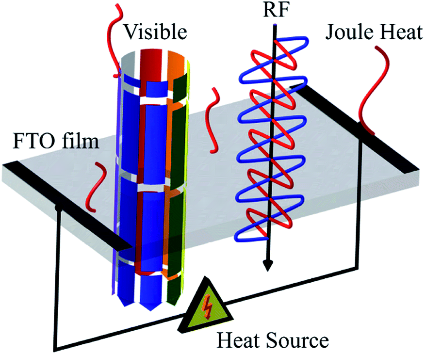 | ||
| Fig. 1 A schematic of a radio-frequency and optically transparent fluorine-doped tin oxide (FTO) film for radome de-icing materials. | ||
Regardless of the type of radome, the higher the optical and RF transmission, the better the communicative performance. At the same time, achieving a higher saturation temperature with low voltage is desirable to remove ice rapidly and efficiently. However, the saturation temperature is proportional to the electrical conductivity while higher electrical conductivity produces lower optical and RF transmission.11 In this study, we analyzed the trade-off relationship between the optical, RF transmission and the heating performance according to the sheet resistance of FTO films. Our investigation of the structural and physical characterizations of FTO films determined the radio-frequency, optical transmission and Joule heating performance. In addition, Dassault CST software was used to validate the RF transmission and temperature distribution of the FTO films.
2. Experimental
The FTO films were deposited on a glass substrate by an ultrasonic spray pyrolysis (USP) system. Fig. 2 shows a schematic design of the USP system (H&Ceon, TX500K), which is composed of an ultrasonic chamber, carrier gas system, reaction furnace, and ventilation.12 Analytical grade tin(IV)tetrachloride pentahydrate (SnCl4·5H2O) and ammonium fluorine (NH4F) were used as precursor materials, and distilled water and ethyl alcohol (C2H5OH) were used as a solvent and stabilizer, respectively. Initially, stoichiometric amounts of the solute were dissolved in deionized water and ethyl alcohol with constant stirring at 70 °C for 1 hour to the clear solution. The ammonium fluorine was consecutively added to the resultant transparent solution under vigorous stirring at 70 °C for 3 hours and then aged for 20 hours at room temperature. Before deposition, substrates were cleaned ultrasonically in deionized water and isopropyl alcohol (IPA) for 10 minutes.13 The solution was sprayed in an ultrasonic chamber (1.6 MHz, 38 V), transferred to a reaction furnace by carrier gas (air, 50 LPM) and deposited onto a glass substrate. The films were deposited in different environments (5 to 20 minutes and 400 to 500 °C) to control the sheet resistance of the FTO film.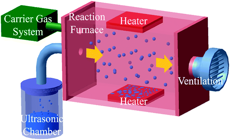 | ||
| Fig. 2 A schematic of ultrasonic spray pyrolysis (USP) system. The horizontally uniform flow allows depositing uniform nanostructure film. | ||
The morphology of the FTO films was observed by FE-SEM (FEI company, Magellan 400) at an accelerated voltage of 15–20 kV. The thickness of the FTO films was analyzed by ellipsometer (J. A. Woollam, Alpha-SE) operating wavelength at 380–900 nm. The electrical and optical properties of FTO films were determined using Hall effect measurement (Nanometrics, HL5500) and ultraviolet-visible spectroscopy (Perkin Elmer, Lambda 1050) with a bare glass film used as a reference. The sheet resistance (Rsh) of the films was measured by a van der Pauw technique using four-point probe equipment (AIT, CMT-SR2000N). The X-band transmission was observed by free-space measurement (HVS Technologies, ver2.16), which is shown in the schematics in Fig. 3a. Joule heating performance was characterized by the saturation temperature at a specific voltage.14 The power was applied for 15 minutes and the size of the effective specimen size was 50 × 50 mm2. The temperature was recorded by a K-type thermocouple at the center of the specimen (Yokogawa, MV2000) as shown in Fig. 3b and c. The temperature was also measured by an IR camera (Topins, FLIR-AX5) to evaluate the temperature distribution of FTO films (Fig. 3d, 1728 Ω sq−1, 60 V) For the de-icing performance test, a sample with a droplet of water on the film surface was put into a temperature and humidity chamber (ENEX Science, EN-STH-604) at −20 °C. After the water had frozen completely, the ice and chamber temperature were recorded by a K-type thermocouple and thermal imaging camera with an applied DC voltage.
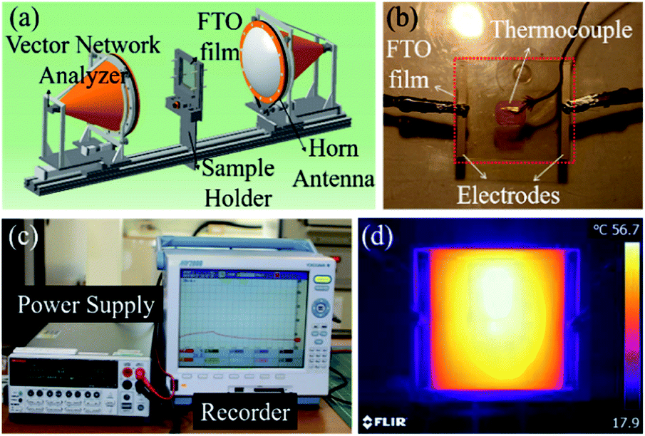 | ||
| Fig. 3 A representation of the experimental setup. (a) The free-space measurement for radio-frequency transmission, (b) the FTO film with electrodes, (c) the power supply and temperature recorder, and (d) the thermal image of an FTO film with a sheet resistance of 1728 Ω sq−1 when 60 V was applied. | ||
3. Results and discussion
3.1. Structural and electrical property
The sheet resistance of FTO films depends on the Hall mobility and carrier concentration. The relationship between the FTO thickness, the resistivity and the sheet resistance are shown in Fig. 4a. The sheet resistance was found to decrease with an increasing film thickness. As shown in the cross-sectional SEM image of the inset in Fig. 4a, it is clear that as the sheet resistance increases, the thickness of the FTO film decreases. The sheet resistance decreased from 5000 to 9 Ω sq−1 with an increase in film thickness from 23 to 529 nm. The decrease in the sheet resistance with an increase in film thickness is consistent with previous reports for undoped and doped SnO2 films.15–17 Fig. 4b shows the variation in Hall mobility and carrier density with the sheet resistance. The Hall mobility of the films shows a gradual decrease from 23.3 to about 8.8 cm2 V−1·s−1 as the sheet resistance increased from 9 to 5000 Ω sq−1. Similarly, the carrier density gradually decreased with a sheet resistance increase. It is a well-known fact that various factors, such as crystallinity, grain size, morphology, porosity, composition, film–substrate interface, etc., play an important role in determining the electrical properties of the films. Therefore, the variation in the electrical parameters of the films described in this study with respect to thickness can be attributed to the difference in their structural properties which we discuss in the following section.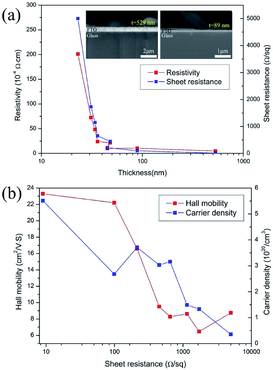 | ||
| Fig. 4 The electrical properties of FTO films. (a) The resistivity (red), and sheet resistance (blue) as a function of the thickness. (b) The Hall mobility (red) and carrier density (blue) as a function of sheet resistance. | ||
Fig. 5 shows the XRD patterns of films with a sheet resistance of 9, 99 and 1147 Ω sq−1. The FTO with 9 Ω sq−1 is polycrystalline and in the tetragonal phase according to the reference pattern of JCPDS (#46-1088). The presence of other phases such as SnO, Sn and SnF2 is not detected. This suggests that fluoride ions are fully incorporated into the tin oxide lattice, without changing the tetragonal structure. Specifically, a close investigation of XRD patterns of 9 Ω sq−1 sample reveals that these diffraction peaks are slightly shifted to a higher angle than the pure SnO2 shown at the bottom (main peak, 38.01° for (200) plane). This implies that the FTO phases are successfully formed as the substitution of a larger O2− (ionic radius 1.40 Å) by a smaller F− (ionic radius 1.36 Å) in the SnO2, which is defined by Bragg's equation (nλ = 2d![[thin space (1/6-em)]](https://www.rsc.org/images/entities/char_2009.gif) sinθ).18 We confirmed that the film with 9 Ω sq−1 has a high degree of crystallinity; however, as the sheet resistance increases, the crystallinity decreases, and the film with 1147 Ω sq−1 exhibits an amorphous film state. The amorphous films have structures characterized by an almost complete lack of periodicity and a tendency to order only in the sense that the atoms are fairly tightly packed together and show a statistical preference for a particular interatomic distance. As a result, the X-ray diffraction pattern shows nothing more than one or two broad maxima without discernible peaks.19 This might be due to the different deposition conditions, i.e., the temperature and time of the film.16 The films have a high degree of crystallinity with low sheet resistance when deposited at a higher temperature (500 °C) and longer deposition time (20 minutes) but the film begins to form an amorphous texture with a higher sheet resistance at a lower deposition temperature and shorter deposition time. The relationship between the deposition conditions and the charge concentrations seems to be related to the results of the phase analysis in the XRD. As shown in Fig. 4b, as the sheet resistance increases, the charge concentration decreases. The FTO is a well-known n-type degenerate semiconductor. In the case of FTO, fluorine (F) is doped into SnO2 lattice where fluorine substitutes for O2− and acts as an electron donor, resulting in an n-type degenerate semiconductor. In the 9 Ω/sq sample, the degree of crystallization is high, so the F− ion is sufficiently substituted into the O2− lattice; therefore, the charge concentration is sufficiently high by generating FO+ and extra e− for the charge compensation. However, as the sheet resistance increases, the degree of crystallinity decreases, so that the sufficient substitution of F− into the O2− lattice does not occur, which diminishes the charge concentration of the films.
sinθ).18 We confirmed that the film with 9 Ω sq−1 has a high degree of crystallinity; however, as the sheet resistance increases, the crystallinity decreases, and the film with 1147 Ω sq−1 exhibits an amorphous film state. The amorphous films have structures characterized by an almost complete lack of periodicity and a tendency to order only in the sense that the atoms are fairly tightly packed together and show a statistical preference for a particular interatomic distance. As a result, the X-ray diffraction pattern shows nothing more than one or two broad maxima without discernible peaks.19 This might be due to the different deposition conditions, i.e., the temperature and time of the film.16 The films have a high degree of crystallinity with low sheet resistance when deposited at a higher temperature (500 °C) and longer deposition time (20 minutes) but the film begins to form an amorphous texture with a higher sheet resistance at a lower deposition temperature and shorter deposition time. The relationship between the deposition conditions and the charge concentrations seems to be related to the results of the phase analysis in the XRD. As shown in Fig. 4b, as the sheet resistance increases, the charge concentration decreases. The FTO is a well-known n-type degenerate semiconductor. In the case of FTO, fluorine (F) is doped into SnO2 lattice where fluorine substitutes for O2− and acts as an electron donor, resulting in an n-type degenerate semiconductor. In the 9 Ω/sq sample, the degree of crystallization is high, so the F− ion is sufficiently substituted into the O2− lattice; therefore, the charge concentration is sufficiently high by generating FO+ and extra e− for the charge compensation. However, as the sheet resistance increases, the degree of crystallinity decreases, so that the sufficient substitution of F− into the O2− lattice does not occur, which diminishes the charge concentration of the films.
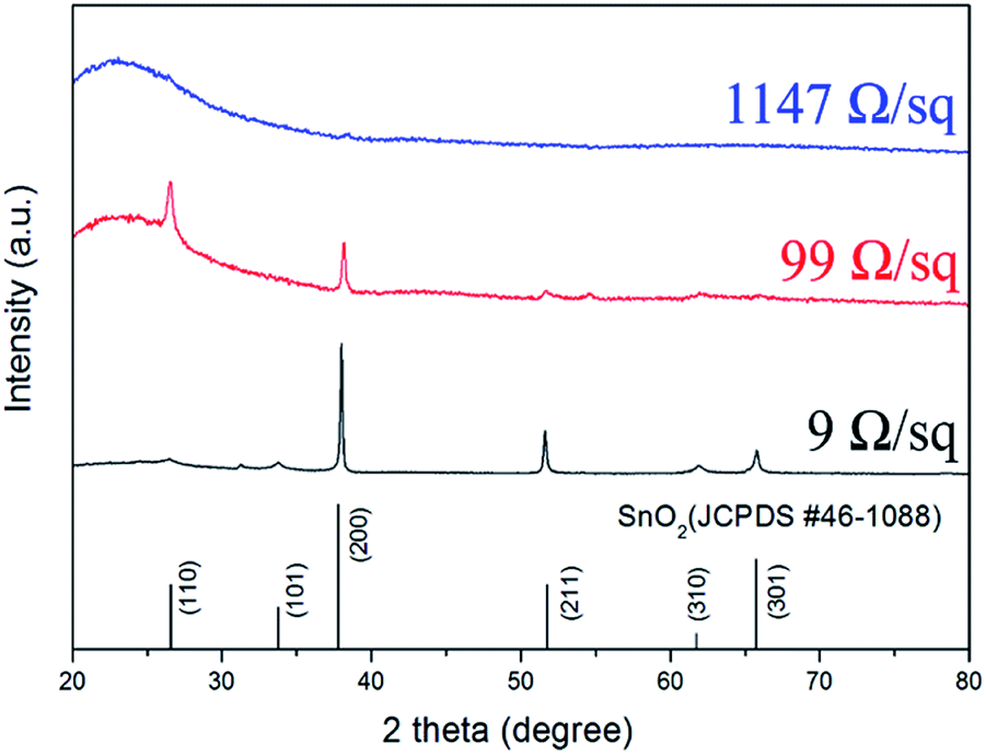 | ||
| Fig. 5 The X-ray diffraction pattern of FTO films with a sheet resistance of 9, 99, and 1147 Ω sq−1. The stick pattern provided is for SnO2 (JCPDS #46-1088). | ||
The carrier mobility (μtot) is described by Matthiessen's rule as follows:20
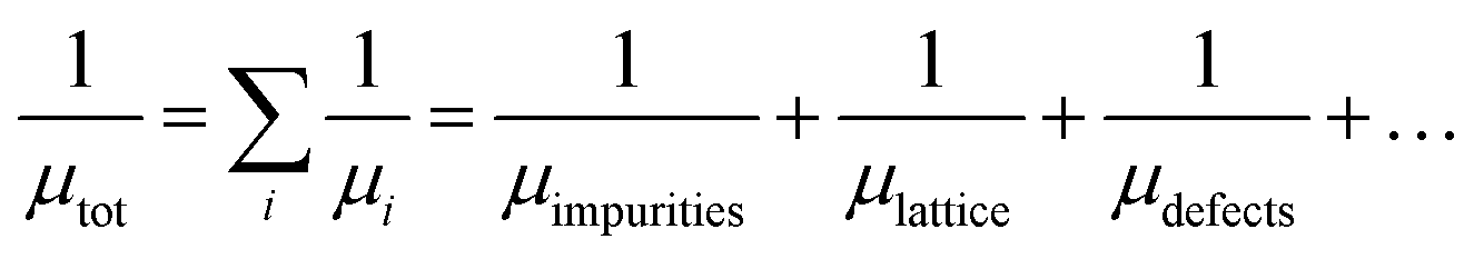
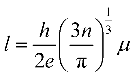
where, h is the Planck constant (6.626 × 10⁻³⁴ J s), e is the electron charge (1.602 × 10⁻¹⁹ C), n is carrier concentration and μ is the Hall mobility. Several properties, including the mean free path of free carriers in FTO with different sheet resistances are calculated and listed in Table 1. In samples with the sheet resistance of 9 and 99 Ω sq−1, the mean path l is in the region of 2.85–3.89 nm, while the crystal size D calculated from the broadening of the diffraction peaks using the Scherrer formula is in the region of 99.2–72.2 nm, and the ratio of the mean free path and the crystal size (l/D) is between 3.89 and 3.70%, which reveals that the mean free path of free carriers is considerably shorter than the grain size of the FTO films. Therefore, the Hall mobility is mainly limited by ionized impurity scattering, which is in agreement with previously reported results.24,25 However, as the sheet resistance increases, the free path decreases in the range of 2.4 and 0.6 nm, which is almost three times that of the lattice parameters (a = b ≈ 4.75 Å, c ≈ 3.198 Å, in the JCPDS #46-1088). The results indicate that Hall mobility may be limited by lattice vibration, resulting in stronger scattering, shorter relaxation time, and finally lower Hall mobility with higher sheet resistance. Therefore, as the sheet resistance increases in the FTO films, the Hall mobility gradually decreases due to the lattice vibration scattering resulted by decreasing the mean free path of carrier electrons. The above analysis confirmed that the electrical resistivity of FTO film is increased by both the effect of the decreasing carrier density and the Hall mobility as the thickness of FTO decreases.
| Sheet resistance (Ω sq−1) | Film thickness (nm) | Carrier concentration (1020/cm−2) | Hall mobility (cm2 V−1 s−1) | Crystalline size, D (nm) | Mean free path, I (nm) | I/D (%) | Optical transmission (%) | RF transmission (%) |
|---|---|---|---|---|---|---|---|---|
| 9 | 529 | 5.51 | 23.3 | 99.2 | 3.9 | 3.89 | 77.3 | 0.219 |
| 99 | 89 | 2.68 | 22.2 | 72.2 | 2.8 | 3.70 | 80.5 | 12.1 |
| 214 | 45 | 3.71 | 16.6 | 2.4 | 85.0 | 29.2 | ||
| 450 | 48 | 3.03 | 9.5 | 1.2 | 86.2 | 50.5 | ||
| 650 | 36 | 3.16 | 8.3 | 1.1 | 85.9 | 59.6 | ||
| 1147 | 34 | 1.49 | 8.6 | 0.9 | 88.5 | 72.5 | ||
| 1728 | 31 | 1.33 | 6.5 | 0.7 | 88.2 | 80.0 | ||
| 5000 | 23 | 0.36 | 8.8 | 0.6 | 91.7 | 90.0 |
3.2. Transmission property
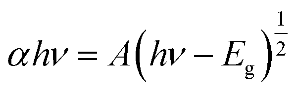
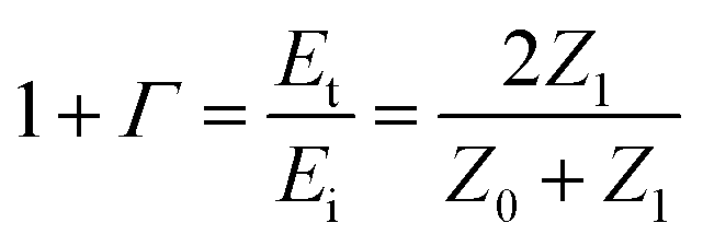
The optical transmission of FTO films at 550 nm is indicated in Fig. 6a. The optical transmission of FTO films steadily increase with an increase in sheet resistance. The FTO films have an average optical transmission from 77.3% to 91.7% with a sheet resistance from 9 Ω sq−1 to 5000 Ω sq−1. This suggests that the increase in film thickness deteriorates optical transmission. The smooth and less textured surface of FTO films with a high sheet resistance increases the optical transmission by suppressing the light scattering. The corresponding optical band gap energy of FTO films are indicated in Fig. 6b. The optical band gap energy is estimated from the Tauc method:13,26where α is the absorption coefficient, h is the Planck constant, ν is the frequency of the incident photon, A is an arbitrary constant, and Eg is the optical band gap energy. The absorption coefficient α is determined by the following equation:
| T ≈ e−αt |
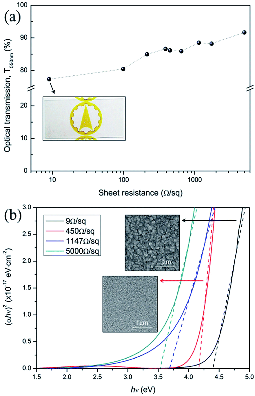 | ||
| Fig. 6 The optical properties of FTO films according to the sheet resistance. (a) The optical transmission at 550 nm and (b) the optical band gap energy with top-view FE-SEM images. The densely packed crystallites contributed to high optical band gap energy. | ||
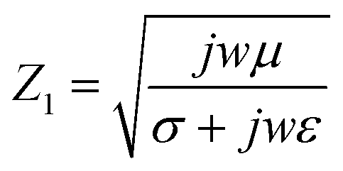
The X-band (8.2–12.4 GHz) transmission results are shown in Fig. 7, which confirms that the simulation and experimental results are in agreement, and the transmission increased from 0.20 to 90.0% by increasing the sheet resistance from 9 to 5000 Ω sq−1. The relation between conductivity and RF transmission can be defined by the transmission line theory.29 The transmission coefficient 1 + Γ is
σ is the conductivity of the medium, ω is the angular frequency of the wave, and ϵ and μ are the permittivity and permeability of the medium, respectively. Basically, as the conductivity of the medium increases, the electromagnetic interference with the incident wave increases. As inferred from the equations, increasing conductivity causes a decrease in the medium impedance and transmission coefficient. Therefore, if the sheet resistance of FTO films is too low, the failure risk of wireless communication is increased due to the low RF signal transmission. Based on the above results, it is clear that in order to ensure an RF transmission with 80.0% or higher, the FTO film must have a sheet resistance higher than 1728 Ω sq−1.
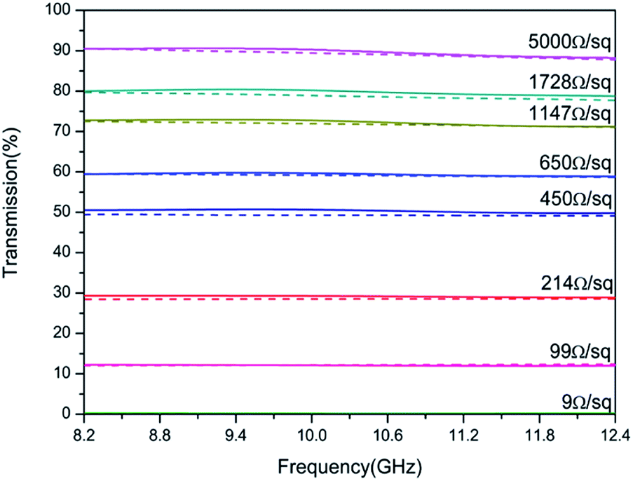 | ||
| Fig. 7 The X-band transmission of FTO films. The solid lines and the dashed lines represent the experimental and simulation transmission of FTO films respectively. As the sheet resistance decreases, the X-band transmission is deteriorated. | ||
3.3. Joule heating performance
Joule heating performance of FTO films is generally indicated by a saturation temperature when DC voltage is applied. Fig. 8a shows the temperature profile of FTO films with a sheet resistance of 1728 Ω sq−1 which has an 80.0% X-band transmission and Fig. 8b shows the saturation temperature of FTO films according to the sheet resistance as the voltage changes. By applying the voltage, the temperature rapidly reaches a saturation temperature within 200 seconds. The response times, which is defined as the time to reach 90% of the saturation temperature (Tsat), are consistent within 87–111 seconds regardless of the applied voltage.30 The saturation temperature remains constant under repeatedly applied voltage, and decreases to room temperature when the voltage is off. The saturation temperature of the fabricated FTO film is strongly dependent on the sheet resistance as well as the applied voltage as illustrated in Fig. 8b. The saturation temperatures were proportional to the spraying time and applied voltage, which can be explained by the relationship ofwhere Tsat is the saturation temperature, P is the electrical power, I is the current, V is the voltage, and R is the resistance.
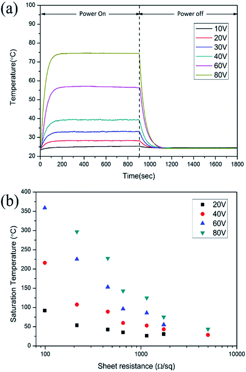 | ||
| Fig. 8 Joule heating performance of FTO films. (a) The temperature profile of FTO films with a sheet resistance of 1728 Ω sq−1 and (b) the saturation temperature of FTO films at room temperature. | ||
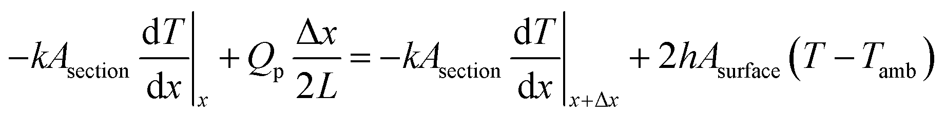
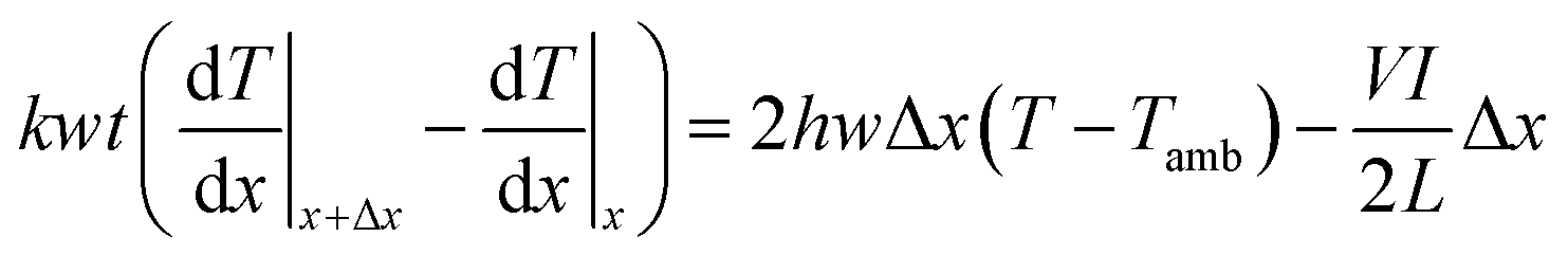
The saturation temperature and temperature distribution by Joule heating on an FTO film are mainly governed by convection and conduction. Considering both conduction and convection, it is necessary to establish an analytical model of the saturation temperature distribution to anticipate the heating performance. Previous studies established the analytical equation for a 1D Joule-heated graphene, and a general heat dissipated 1D element.31,32 However, the former emphasizes the effect of the substrates, ignoring heat convection, and the latter excludes the heat source by Joule heating. By combining the adequate conditions, the analytical model for saturation temperature distribution can be derived. To start with, two assumptions are needed for simplification. First, the electrodes are heated like FTO films, and the temperature of end contact is identical to the ambient temperature. As a boundary condition, the temperature of very end contact can approximate the ambient temperature. Second, the temperature of the substrate is identical to that of the FTO film. Even though the glass is one of the representatives of an insulator, the thickness of the glass is thin enough (0.5 mm) to dissipate the heat. Fourier's law for 1D conduction is:
| Qcond_in + Qp = Qcond_out + Qconv |
where k is the thermal conductivity (W m−1 K−1) of a glass, h is the convective heat transfer coefficient (W m−1 K−1). Again,
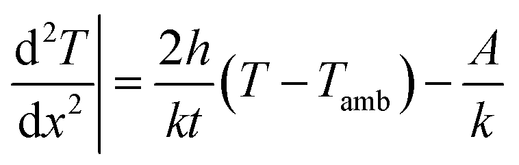
where V, and I are the input voltage (V) and current (A). Set VI/(2wtL) as A:
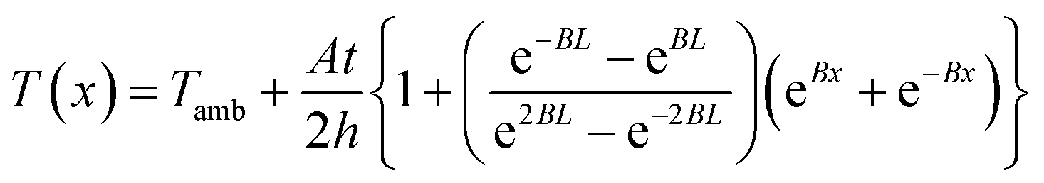
where A is the power dissipated per unit volume (W m−3). From the general solution of the 2nd order differential equation and boundary conditions, the saturation temperature T at length x from the center is expressed as:
where B is (2h/kt)1/2. This is the analytical equation of temperature distribution by Joule heating on an FTO film. Fig. 10a shows the comparison between the analytical, experimental, and simulation saturation temperature distribution (Tsat − Tamb) of an FTO film with a sheet resistance of 1728 Ω sq−1 with a convective heat transfer coefficient 7.87 W m−2 K−1. The convective heat transfer coefficient can vary with the material property from surface roughness, grain growth, and oxidation progress, etc. Therefore, the optimized convective heat transfer coefficient can differ from the sheet resistance of FTO films. Fig. 10b shows the thermal simulation of FTO films with a sheet resistance of 1728 Ω sq−1 with a convective heat transfer coefficient of 7.87 W m−2 K−1 when 60 V is applied by CST MPS software. Note that there is only an inconsiderable difference between analytical and simulation saturation temperature distribution. On the other hand, there is a minor difference between analytical and experimental results, which might be due to two main reasons: non-uniform deposition, and inconsistent convective heat transfer coefficient. Nevertheless, the analytical equation is relevant to easily anticipate the saturation temperature distribution of a Joule-heated FTO film. Since it primarily requires given properties, such as the material properties of a substrate, supplied power, and dimensions, it is simple to depict the saturation temperature distribution. However, there are restrictions to apply this equation: it requires a thin enough substrate to dissipate the heat and a consistent convective heat transfer coefficient. Since convection is the main governing heat transfer mechanism, the importance of the convective heat transfer coefficient cannot be emphasized enough.
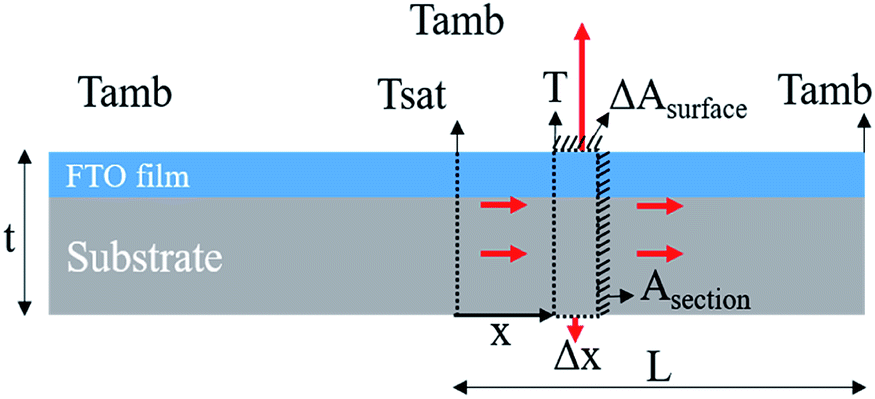 | ||
| Fig. 9 A schematic of 1D heat transfer in an FTO film. The infinitely small volume is a system and the heat is transferred by conduction and convection to the surroundings. | ||
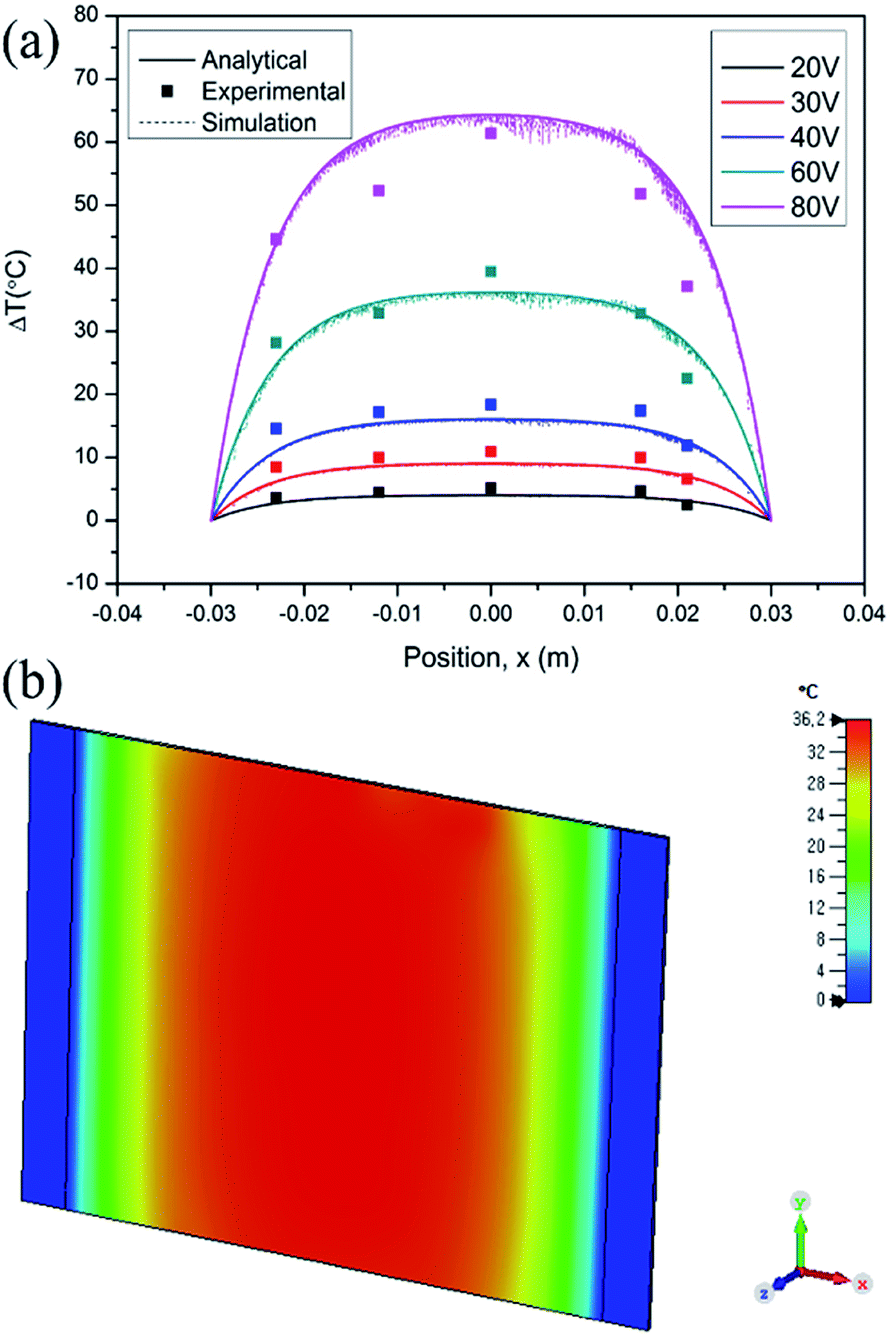 | ||
| Fig. 10 (a) The comparison between the analytical, experimental, and simulation saturation temperature distribution (Tsat − Tamb) of an FTO film with a sheet resistance of 1728 Ω sq−1 and (b) its thermal simulation when 60 V was applied. | ||
3.4. De-icing demonstration
Fig. 11a shows the temperature profile of an FTO film with a sheet resistance of 1728 Ω sq−1 at −20 °C according to the voltage change. As with the room temperature, the saturation temperature is achieved within 200 seconds after applying the power, and it reached from −18.7 to 36.1 °C for 10 to 80 V. As indicated in the analytical equation of temperature distribution, it is confirmed that the temperature difference (Tsat − Tamb) has nothing to do with the ambient temperature (Tamb) as shown in Fig. 8a and 11a. The maximum error of the temperature difference is 5.0 °C when 80 V is applied which seems negligible. In the same way, the response time is 83–109 seconds, which is identical to that of room temperature. That is because the response time is related to the substrate type, the boundary conditions, and the convection rate, etc., not the ambient temperature.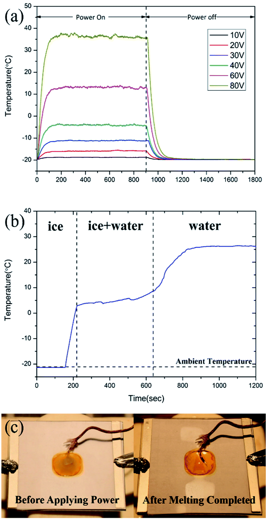 | ||
| Fig. 11 The de-icing demonstration of an FTO film. (a) The temperature profile of FTO films with a sheet resistance of 1728 Ω sq−1 at −20 °C according to the voltage change without ice. (b) The ice temperature when 80 V is applied to the FTO film with a sheet resistance of 1728 Ω sq−1 at −20 °C. (c) The ice images before and after the power was applied. | ||
In this study, among the FTO films with the X-band transparent (transmission above 80.0%), the FTO film with the lowest sheet resistance, which is the FTO film with sheet resistance 1728 Ω sq−1 was selected to de-icing materials. The input voltage for de-icing is minimized (<100 V) for the stable power supply. Fig. 11b shows the temperature of a water droplet when 80 V is applied to the FTO film until the ice melted completely. The FTO film with a sheet resistance of 1728 Ω sq−1 with a drop of water was placed in the humidity and temperature chamber at −20 °C to simulate the cold temperature of the operating environment. After the power was applied, it took only 65 seconds to reach 2.8 °C. The unstable temperature increase, from 2.8 to 9.1 °C, where the thermal energy was converted into latent heat. After melting was completed, the temperature saturated into 26.5 °C, which represented a lower temperature than in Fig. 11a due to the water droplet.
The de-icing performance of FTO films is highly dependent on Joule heating performance. From Fig. 11b, when the ice on FTO film accreted, the voltage was applied to melt the ice. The temperature rapidly increases. The heat transferred to ice is 50.85 kJ kg−1 since the heat capacity of ice is about 2.11 kJ kg−1 K−1 and temperature change is −21.3 to 2.8 °C. At the state of phase change, the heat transferred is 355 kJ kg−1 since it is the latent heat of fusion of water. After melting completed, the water droplet converged into saturation temperature. The heat transferred is 67.30 kJ kg−1 since the heat capacity of water is about 4.18 kJ kg−1 K−1 and temperature rose from 9.1 to 25.2 °C.
To apply FTO films as radome de-icing materials, a heating power density should be in the range of common aircraft power specifications. It is known that the heating power density for common ship or aircraft is 0.386 W cm−2.3 In the de-icing process of the FTO film with a sheet resistance of 1728 Ω sq−1, from the Ohm's law, the heating power density is 0.148 W cm−2 for input voltage 80 V. These results confirmed that the FTO film with a sheet resistance of 1728 Ω sq−1 can eliminate ice on the surface with 80.0% RF transmission within the range of power available.
4. Conclusions
We fabricated a robust FTO film by ultrasonic spray pyrolysis and evaluated its application as a radome de-icing material. Based on an RF transmission test (from 8.2 to 12.4 GHz) and simulations, the RF transmission was about 80.0% for the FTO film with a sheet resistance of 1728 Ω sq−1 and optical transmission of 88.2%. The de-icing performance of the FTO film was evaluated at −20 °C, and the efficient removal of ice under such cold conditions was demonstrated. To the best of our knowledge, no previous research has investigated such an RF transparent performance combined with Joule heating performance of FTO films. Based on the above results, we believe that, with modification and optimization of the process parameters, the FTO films will become promising materials for lightweight broadband radome de-icing applications. Furthermore, the FTO films will be able to expand to de-icing materials for a reconnaissance, surveillance window due to its high optical transmission and durability.Conflicts of interest
There are no conflicts to declare.Acknowledgements
This work was supported by the Agency for Defense Development, Republic of Korea and Defense Acquisition Program Administration, Republic of Korea.Notes and references
- G. Lance, MPDigest, 2008, 1–4 Search PubMed.
- K. Szilder and W. Yuan, Progress in Flight Physics, 2017 Search PubMed.
- V. Volman, J. M. Tour, Y. Zhu and A. R. O. Raji, 2013 IEEE International Symposium on Phased Array Systems and Technology, 2013 Search PubMed.
- A. E. Hassanien, H. M. Hashem, G. Kamel, S. Soltan, A. M. Moustafa, M. Hammam and A. A. Ramadan, International Journal of Thin Films Science and Technology, 2016, 5, 55–65 Search PubMed.
- B. Liao, S. H. Chan, C. C. Lee, S. H. Chen and D. Chiang, Optical Interference Coatings, 2013 Search PubMed.
- E. Elangovan and K. Ramamurthi, Thin Solid Films, 2005, 476, 231–236 CrossRef CAS.
- B. R. Koo, D. H. Oh, D. H. Riu and H. J. Ahn, ACS Appl. Mater. Interfaces, 2017, 9, 44584–44592 CrossRef CAS.
- M. Obaida, I. Moussa and M. Boshta, Int. J. ChemTech Res., 2015, 8, 239–247 CAS.
- V. Bilgin, I. Akyuz, E. Ketenci, S. Kose and F. Atay, Appl. Surf. Sci., 2010, 256, 6586–6591 CrossRef CAS.
- P. S. Shewale, S. I. Patil and M. D. Uplane, Semicond. Sci. Technol., 2010, 25, 15008 CrossRef.
- G. Haacke, J. Appl. Phys., 1976, 47, 4086–4089 CrossRef CAS.
- R. Taziwa and E. Meyer, Fabrication of TiO2 Nanoparticles and Thin Films by Ultrasonic Spray Pyrolysis: Design and Optimization, in Pyrolysis, InTech, London, UK, 2017 Search PubMed.
- C. Kahattha, R. Noonuruk and W. Pecharapa, Integr. Ferroelectr., 2016, 175, 138–145 CrossRef CAS.
- A. Y. Kim, M. K. Kim, C. Hudaya, J. H. Park, D. Byun and J. C. Lim, Nanoscale, 2016, 8, 3307–3313 RSC.
- G. Sanon, R. Rup and A. Mansingh, Phys. Status Solidi, 1991, 128, 109–116 CrossRef CAS.
- J. Dutta, J. Perrin, T. Emeraud, J. M. Laurent and A. Smith, J. Mater. Sci., 1995, 30, 53–62 CrossRef CAS.
- H. D. Waal and F. Simons, Thin Solid Films, 1981, 77, 253–258 CrossRef.
- K. S. Ramaiah and V. S. Raja, Appl. Surf. Sci., 2006, 253, 1451–1458 CrossRef CAS.
- B. D. Cullity, Elements of X-ray Diffraction, Pearson, 2001 Search PubMed.
- S. Kasap and P. Capper, Springer Handbook of Electronic and Photonic Materials, Springer, 2006 Search PubMed.
- B. H. Kim, C. M. Staller, S. H. Cho, S. Heo, C. E. Garrison, J. Kim and D. J. Milliron, ACS Nano, 2018, 12, 3200–3208 CrossRef CAS.
- L. T. C. Tuyen, S. R. Jian, N. T. Tien and P. H. Le, Materials, 2019, 12, 1665 CrossRef CAS.
- S. Noguchi and H. Sakata, J. Phys. D: Appl. Phys., 1979, 13, 1129–1133 CrossRef.
- J. K. Yang, B. Liang, M. J. Zhao, Y. Gao, F. C. Zhang and H. L. Zhao, Sci. Rep., 2015, 5, 15001 CrossRef CAS.
- S. Y. Lee and B. O. Park, Thin Solid Films, 2006, 510, 154–158 CrossRef CAS.
- Z. Banyamin, P. Kelly, G. West and J. Boardman, Coatings, 2014, 4, 732–746 CrossRef.
- G. A. Velazquez-Nevarez, J. R. Vargaas-Garcia, L. Lartundo-Rojas, F. Chen, Q. Shen and L. Zhang, J. Wuhan Univ. Technol.-Materials Sci. Ed., 2016, 31, 48–51 CrossRef CAS.
- N. S. Subramanian, M. Jeyachandran and S. Ramamurthy, Sci. Focus J., 2019, 40(2) CrossRef.
- D. M. Pozar, Microwave Engineering, 2011 Search PubMed.
- D. Sui, Y. Huang, L. Huang, J. Liang, Y. Ma and Y. Chen, Small, 2011, 7, 3186–3192 CrossRef CAS.
- K. R. Chandran, Int. J. Heat Mass Transfer, 2015, 88, 14–19 CrossRef.
- M. Tecpoyotl-Torres, J. Micro/Nanolithogr., 2009, 8, 023020 CrossRef.
- F. P. Incropera, D. P. DeWitt, T. L. Bergman and A. S. Lavine, Polysilicon thermal microactuators for heat scavenging and power conversion, Hoboken, 2017 Search PubMed.
| This journal is © The Royal Society of Chemistry 2020 |