DOI:
10.1039/D0RA06541B
(Paper)
RSC Adv., 2020,
10, 40467-40479
Synthesis and characterization of Mg-doped ZnO thin-films electrochemically grown on FTO substrates for optoelectronic applications
Received
28th July 2020
, Accepted 23rd October 2020
First published on 6th November 2020
Abstract
Mg-doped ZnO (MZO) thin films were successfully fabricated on fluorine-doped tin-oxide (FTO)-coated glass substrates by an electrochemical deposition method using aqueous electrolytes of 80 mM Zn(NO3)2 with different concentrations of Mg(NO3)2. The effects of Mg doping concentration on the electronic, microstructural, morphological, optical and electrical properties of the prepared films were investigated. The results of the Mott–Schottky (M–S) analysis revealed that the charge carrier density of n-type MZO films increases considerably when increasing the amount of Mg. As Mg concentration increased the Fermi level energy was also found to be increased by inclusion of Mg doping, which was confirmed by negative shifting of the flat band potential. XRD analysis showed that both undoped and Mg-doped ZnO thin films have a polycrystalline nature and hexagonal wurtzite structure with preferential orientation along the (002) axis. It is evident that the intensity of the (002) peak decreased with increasing Mg concentration. From scanning electron microscopy (SEM) analysis, it was found that when the amount of Mg concentration was increased in the solution, a decrease in the size of the grains was observed. The optical transmittance was found to be very high (∼85%) in the visible region of the solar spectrum. When the Mg content in the ZnO system was increased, a blue shifting of the absorption edge of the films was observed. The result of I–V measurements showed that the Mg doping was found to lead to an enhancement of the electrical properties of MZO thin films and the design of high-performance transparent conductive oxide (TCO) material.
1. Introduction
In recent years, transparent conductive oxide (TCO) based thin films have been studied extensively due to their unique properties and for potential applications in optoelectronic devices such as high light-emitting diodes, electronic paper displays, liquid crystal displays, touch panels, plasma displays, and thin-film solar cells.1 Indium tin oxide (ITO) is typically used as a TCO material owing to its low resistivity of about 1 × 10⁻⁴ Ω cm and high optical transmittance (∼90%) in the visible wavelength range, 400–800 nm.2 However, concerns over limited indium (In) resources have recently resulted in increased manufacturing costs. Low-cost and high-performance TCO thin films are thus essential and more desirable as the substituent in novel optoelectronic devices. In recent years, a considerable amount of research has been conducted investigating the substitution of TCO material for ITO thin films.3,4 Among many kinds of TCO films, zinc oxide (ZnO) has drawn considerable interest and is a promising alternative to the commonly used ITO because of its intrinsic physical and optical properties, easy doping characteristics and potential values for optoelectronic applications due to its non-toxicity, abundance, and low-cost.5,6 ZnO is an n-type II–VI semiconducting compound with a wide direct bandgap of approximately 3.3 eV and a large excitonic binding energy of 60 meV. Hall mobility in ZnO single crystal is on the order of 200 cm2 V−1 s−1 at room temperature. What is more, this TCO film is easy to implement doping due to its low epitaxial growth temperature. Recently, several researchers have paid tremendous attention to doping of a wide range of elements (Mg, Fe, Ni, Ag, Mn, Cu, Al, Ga etc.) in ZnO.7–10 The selection of the dopant element is aimed to improve the properties of ZnO thin films for a particular practical application. Magnesium is an appealing doping element among the above mentioned elements, because the ionic radius of Mg2+ (0.057 nm) is close with Zn2+ (0.06 nm) in ZnO films, and MgO has a larger bandgap (7.7 eV) than that of ZnO material,7,11 which means that the replacement of zinc by magnesium will not induce significant lattice distortion, and the optical bandgap energy of MZO films can be finely modulated from 3.4 (ZnO bandgap energy) to 7.8 eV (MgO bandgap energy), depending on the doping composition.11 Mg-doped ZnO (MZO) is generally formed when Zn2+ in ZnO is partially replaced by Mg2+, and the similar radii of Mg and Zn ions avoid the formation of high-density defects resulting from the stress mismatch. In addition, the phase diagram of MgO–ZnO indicates the solubility of MgO in ZnO is less than 4% in bulk and in thin films and the solubility can be as high as 33%.12 Therefore, doping ZnO with magnesium form another attractive material of MZO seems even more interesting TCO film for optoelectronic and displays device applications.13,14
In recent years, an increasing number of studies have focused on the growth and properties of the ZnO and MZO thin films fabricated by various techniques. Fabrication of MZO film for optoelectronic applications is generally done through vapor phase deposition with or without catalysts. Various methods that have been used to prepare ZnO and MZO films are molecular beam epitaxy, pulsed laser deposition, vapor liquid solid phase growth, metal–organic vapor phase epitaxial (MOVPE), hydrothermal and sol–gel growth. Huang et al.15 studied the structural and optical properties of MZO thin films deposited by sol–gel method. They reported that a secondary phase of MgO can be evolved with a ratio of Mg![[thin space (1/6-em)]](https://www.rsc.org/images/entities/char_2009.gif) :Zn = 0:08, and the bandgap energy of ZnO increase with increasing Mg concentration. Gruber et al.16 investigated the properties of MZO epilayers and ZnO–MZO quantum well structures grown by MOVPE. An increase in the optical bandgap energy of 200 meV with 10% Mg doping composition was achieved.16 Arshad et al.17 synthesized the MZO thin films by a wet chemical route. They reported that the Mg doping inhibited the growth of particle size, increased the optical gap and enhanced the visible photoluminescence (PL) emission. In addition, Chiu et al.18 improved the energy bandgap of MZO after post-annealing at 700 °C and showed good device characteristics with mobility of 1.32 cm2 V−1 s−1 and on/off ratio of 2.65 × 10⁴. Moreover, Karthick et al.19 demonstrated in their study on the influence of Mg doping on the functional properties of ZnO thin films prepared by sputtering that the blue shift in the PL emission for MZO thin films might be the reason of the modulation of bandgap with suppression of defect center by the inclusion of Mg doping. They also reported that a significant change in surface morphology of the films was observed with Mg doping.19 In an another study, Mia et al.20 demonstrated in their work on the fabrication of MZO thin films by using sol–gel spin coating technique that the sharp absorption edge of ZnO exhibited blue-shifts and the crystallite size increased with the increase of Mg doping content. Unpredictably, only a few papers are reported on the fabrication of MZO by electrodeposition method. Because of its less time consumption, high efficiency, high yield, and economy, electrodeposition is particularly attractive technique for thin films fabrication in various applications. Electrochemical deposition method is the most effective since it is capable to perform doping incorporation and control the electrical and optical properties of films by monitoring and adjusting the deposition conditions as well as the different ion proportions in the electrolyte solutions.21–23 After adjusting these parameters, high-quality undoped and Mg-doped ZnO thin films were successfully deposited on fluorine-doped tin oxide (FTO) substrate by the ECD technique. The influence of doping with Mg on the electrochemical, structural, optical, morphological and electrical properties of the electrodeposited thin films systematically investigated, and the obtained results are discussed in detail in this report.
:Zn = 0:08, and the bandgap energy of ZnO increase with increasing Mg concentration. Gruber et al.16 investigated the properties of MZO epilayers and ZnO–MZO quantum well structures grown by MOVPE. An increase in the optical bandgap energy of 200 meV with 10% Mg doping composition was achieved.16 Arshad et al.17 synthesized the MZO thin films by a wet chemical route. They reported that the Mg doping inhibited the growth of particle size, increased the optical gap and enhanced the visible photoluminescence (PL) emission. In addition, Chiu et al.18 improved the energy bandgap of MZO after post-annealing at 700 °C and showed good device characteristics with mobility of 1.32 cm2 V−1 s−1 and on/off ratio of 2.65 × 10⁴. Moreover, Karthick et al.19 demonstrated in their study on the influence of Mg doping on the functional properties of ZnO thin films prepared by sputtering that the blue shift in the PL emission for MZO thin films might be the reason of the modulation of bandgap with suppression of defect center by the inclusion of Mg doping. They also reported that a significant change in surface morphology of the films was observed with Mg doping.19 In an another study, Mia et al.20 demonstrated in their work on the fabrication of MZO thin films by using sol–gel spin coating technique that the sharp absorption edge of ZnO exhibited blue-shifts and the crystallite size increased with the increase of Mg doping content. Unpredictably, only a few papers are reported on the fabrication of MZO by electrodeposition method. Because of its less time consumption, high efficiency, high yield, and economy, electrodeposition is particularly attractive technique for thin films fabrication in various applications. Electrochemical deposition method is the most effective since it is capable to perform doping incorporation and control the electrical and optical properties of films by monitoring and adjusting the deposition conditions as well as the different ion proportions in the electrolyte solutions.21–23 After adjusting these parameters, high-quality undoped and Mg-doped ZnO thin films were successfully deposited on fluorine-doped tin oxide (FTO) substrate by the ECD technique. The influence of doping with Mg on the electrochemical, structural, optical, morphological and electrical properties of the electrodeposited thin films systematically investigated, and the obtained results are discussed in detail in this report.
2. Materials and methods
The electrodeposition of Mg-doped ZnO (MZO) thin films was performed in an electrochemical cell with three-electrode containing saturated calomel electrode (SCE, +0.241 V vs. standard hydrogen electrode, NHE) as reference electrode, platinum (Pt) wire as a counter electrode, and fluorine-doped tin oxide glass substrate (FTO) as a working electrode with a resistivity of 70–90 Ω sq−1 and an exposed area of 1 × 2 cm2. Prior to any deposition step, the FTO glass substrates were rinsed with distilled water and then degreased in ultrasonic baths with acetone (CH3COCH3) and methanol (CH3OH) for 15 min to remove the surfaces contamination and finally rinsed with distilled water. The deposition of Mg-doped ZnO thin films was carried out potentiostatically at −1.30 V vs. SCE, directly on pre-cleaned FTO glass substrate, by using a computer-controlled potentiostat/galvanostat (VoltaLab-PGZ-301) as a potential source. The growth electrolytes used for preparing MZO thin films contained 80 mM zinc nitrate Zn(NO3)2 and different amounts of magnesium nitrate Mg(NO3)2 as dopants source. The Mg dopants content percentages (x at%) in MZO thin films were estimated at 1, 2, 3, 4 and 5% of Mg for 0.8, 1.6, 2.4, 3.2 and 4 mM Mg(NO3)2, respectively. The electrolyte temperature was kept constant at 70 °C using a controlled temperature water bath. No stirring was carried out during the experiments. The depositions were performed under computer control by chronocoulometric technique which involves the measurement of the charge quantity (Q) collected at the working electrode vs. time response following an applied potential step. The nominal thickness of the deposited films (d) was estimated from the charge quantity (Q) according to Faraday's formula. Each film was deposited by passing 0.53 C cm−2, resulting in a film thickness of about 0.4 μm. This value was checked by a profilometry measurement using a stylus profilometer (Tencor alpha step D500) and found to be of approximately 0.3 μm. Here, it is important to note that the thickness of MZO thin films was found to be independent of the Mg doping level. However, the electrodeposition duration of MZO layers was decreased with the increase of the Mg doping content as indicated in the chronocoulometry curves (note shown here). This result reveals that the deposition of Mg-doped ZnO layers was faster and easier with the inclusion of Mg doping. The observed deviation of the measured thicknesses values and the theoretical estimate is due to the assumption that all the electronic charges flowing through electrolytic cell contribute in the deposition of MZO thin films. The assumption did not consider the electronic charges associated with the electrolysis of water into its constituent ions. After deposition, the MZO thin films were rinsed systematically with distilled water and then air-dried.
The prepared films were characterized by Philips X'Pert PRO X-ray diffractometer with monochromated CuKα1 (λ = 1.54 nm) wavelength to get the structural insights in θ/2θ scan mode. Using scanning electron microscope (SEM, Joel JSM-7001F) and atomic force microscope (AFM, MFP-3D Asylum Research) the observation of the surface and the morphology images were obtained. The optical properties were evaluated at room temperature with a UV-Shimadzu 2600/2700 spectrophotometer. The background contribution of FTO glass substrates to the absorption spectra was eliminated. The voltammetry measurements were performed by a computer controlled VoltaLab 40-PGZ-301 potentiostat/galvanostat connected to a standard three-electrode system. Semiconducting properties were investigated at room temperature through Mott–Schottky (M–S) measurements by employed a frequency of 200 Hz in 1 M NaNO3 solution. The current–voltage (I–V) characteristics of the deposited samples were evaluated at ambient temperature in both forward and reverse bias conditions.
3. Results and discussion
The growth mechanism of the electrodeposited ZnO films from nitrates baths can be simply described by the eqn (1) and (2). During the deposition process, nitrate ions (NO3−) were reduced to nitrite ions (NO2−) according to eqn (1) in the presence of Zn2+ ions, which adsorbed on the surface of the working electrode. Consequently, excess hydroxyl ions (OH−) were produced, giving rise to increasing the local pH value of the deposition electrolyte of ZnO. This, in turn, should facilitate the precipitation of zinc ions (Zn2+) as zinc hydroxide Zn(OH)2. The generated metal hydroxide were dehydrated spontaneously into zinc oxide as described in eqn (2) at suitable temperature baths with high pH value.21–23| | |
NO3(aq)− + H2O(l) + 2e− → NO2(aq)− + 2OH(aq)− (E° = 0.244 VNHE)
| (1) |
| | |
2OH(aq)− + Zn(aq)2+ → Zn(OH)2(s) → ZnO(s) + H2O(l)
| (2) |
In order to inspect the effect of Mg doping in the electrochemical behavior of the electrodeposition mechanism of ZnO, the voltammetric measurements were carried out. Fig. 1a showed typical cyclic sweep voltammetry (CSV, cathodic) curves recorded at 70 °C in the potential range of 0 to −1.5 V vs. SCE onto FTO substrate immersed in the growth solutions of MZO films. The scan rate was maintained at 50 mV s−1 and the resulted current was monitored. It can be seen that all the CV scans reveal the same appearance where an obvious cathodic current starts to flow near −0.70 V vs. SCE was noted. This current flow was assigned to the electrochemical reducing process of nitrate ions (NO3−). As the applied potential was increased during the cathodic sweep, the current flow showed a tendency to increase, revealing the increase of the reduction rate of nitrate ions, which in turn leads to an equivalent increase in the growth rate of ZnO on the basis of the reactions described in eqn (1) and (2). The increased cathodic current flow with the increase of the applied potential was even more pronounced when the magnesium nitrates Mg(NO3)2 were added to the growth electrolyte of ZnO. This was believed to be attributed to the ion migration ability improvement and the hydroxyl ions (OH−) production near the surface of the substrate, both of which are in favor of the formation of ZnO.21–24 The CV data revealed also that the onset of a cathodic current occurred at more positive potentials in the Mg containing electrolytes. Such behavior is very similar to the Langmuir type adsorption observed in the catalytic role of Zn2+ ions in nitrates reduction by Yoshida et al.25 The CV analysis provided, thus, strong evidence that Mg2+ is analogous to Zn2+ and other metallic cations adsorbing onto the electrode surface and acting as a catalyst for the reduction of nitrates ions in aqueous solutions as shown in Fig. 1b. This is expected to maintain uniform growth of MZO thin films at the very large current density created by high Mg concentrations. These findings confirmed that the deposition process of the ZnO is faster and easier with the contribution of Mg doping.
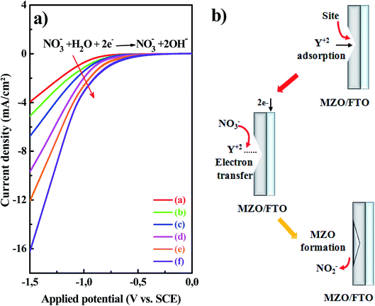 |
| | Fig. 1 (a) Cyclic sweep voltammetry plots (CSV, cathodic) recorded at 70 °C for FTO substrate immersed in the electrolytes with Mg concentrations. The applied voltage was swept from 0 to −1.5 V vs. SCE with a scan rate of 50 mV s−1. (b) Illustration of the electrodeposition process of MZO from Zn(NO3)2 and Mg(NO3)2 bath involving the catalytic reduction of nitrates by adsorbed Y2+ ions (Y = Mg, Zn). | |
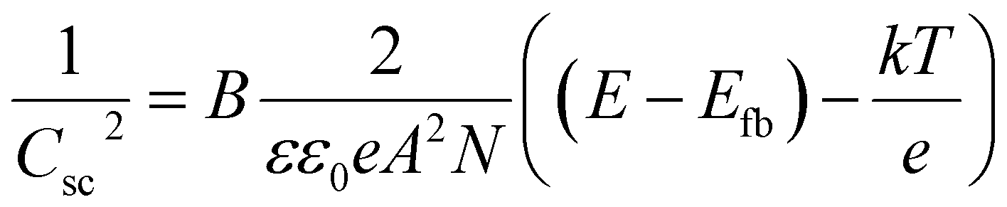
The impedance analysis was performed over a scanned range of applied biases voltage to enable the Mott–Schottky (M–S) measurements, based on examining the semiconductor electrode/solution contacts and determining the capacitance of the space charge region (Csc) under depletion condition as a function of the electrode biases. In fact, the semiconductor material/electrolyte interface can be treated as two layers: the space charge layer and double layer, which in turn includes the Gouy and the Helmholtz layer.26 Both of these layers contribute to the total capacitance of the semiconductor material/electrolyte interface, but as the capacitance of the double layer is far greater than that of the capacitance of the space charge layer, its contribution is conventionally neglected. Thus, the total capacitance value found by impedance analysis is presumed to be the value of the space charge capacitance (CT ∼ Csc). The Mott–Schottky measurements are based on the apparent capacitance (approximated the capacitance of the space charge region) dependence of the applied biases across the semiconductor electrode/electrolyte interface as describing the following equation:27
| |
 | (3) |
where,
Csc stands for the capacitance of the space charge layer,
e is the elementary charge value (
e = 1.6 × 10
−19 C),
N represents the charge carrier density (electron donor density for n-type semiconductor or hole acceptor density for a p-type semiconductor),
ε0 is the vacuum permittivity (
ε0 = 8.86 × 10
−12 F m
−1),
ε the dielectric constant of the semiconductor (
ε is 8.5 for ZnO
28),
E and
Efb denote the applied and the flat band potential, respectively;
k is the Boltzmann's constant (1.38 10
−23 J K
−1),
T is the absolute temperature (
T = 298 K),
A is the exposed electrode area (1 cm
2). B equals +1 and −1 for n-type and p-type semiconductors, respectively. Doping types of semiconductor materials can be deduced from the slope of the straight line of M–S plots (
C−2 vs. E), where, the positive slope is for n-type doping while the negative slope is for p-type doping.
29 The potential at which the straight lines of M–S plots intersect the applied potential axis (infinite capacitance,
i.e.,
C−2 = 0) yields the flat band potential (
Efb) and the gradients give the charges carrier density as represented in
eqn (4).
| | |
N = (2/A2eεε0)[d(1/C2)/dV]−1
| (4) |
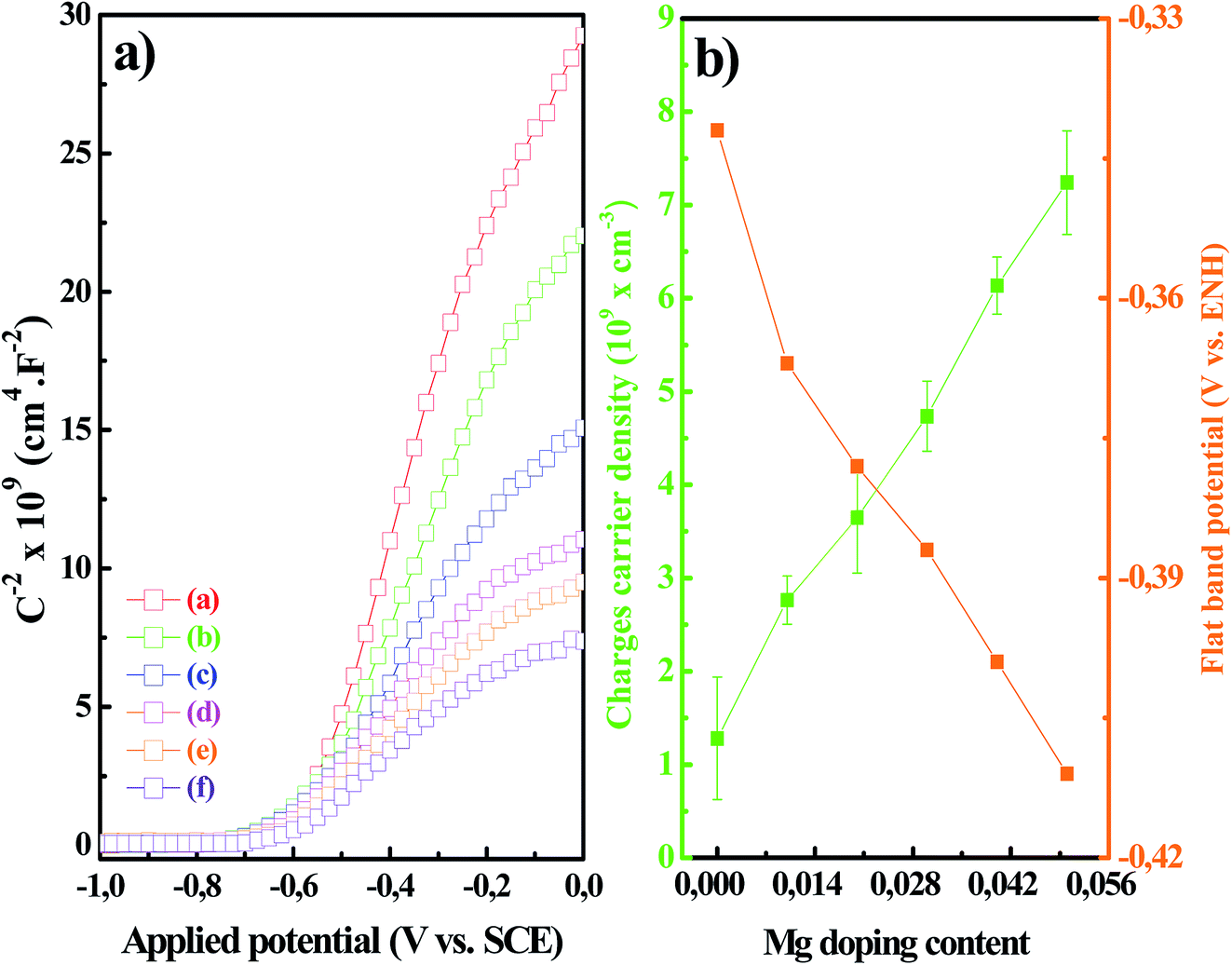
Fig. 2a shows M–S plots (C−2 vs. E) obtained for MZO thin films with Mg at different concentrations. The corresponding fitting results are given in Table 1. The negative slope observed in Fig. 2a indicated that all the MZO films possessed n-type characteristics. The donor carrier density (ND) of the Mg-free-ZnO thin film was estimated to be 1.228 ± 0.657 ×1020 cm−3. This value is higher about one order of magnitude than the values commonly reported in the literature for regular electrodeposited n-type ZnO thin films (∼1019 cm−3).30,31 Our electrodeposition condition, therefore, appears to produce ZnO thin films that are intrinsically heavily doped (e.g. oxygen vacancies or zinc interstitial defects). Furthermore, the ND values were increased from 2.763 ± 0.259 ×10²⁰ to 7.242 ± 0.566 ×1020 cm−3 as the Mg dopants content were increased within the MZO thin films from 1 to 5%, respectively. A similar trend was observed for Mg-doped ZnO thin films in previously published studies.32,33 The sevenfold increase of the charges carrier density of MZO samples was believed to be due to the incorporation of Mg into the ZnO structure by substituting Zn atoms. In fact, the incorporation of Mg ions in ZnO lattice has been discussed extensively by employing a variety of experimental and numerical approaches, that have common outputs as a result of the substitutional replacement of Zn ions with Mg ions in ZnO host lattice.32,34 First-principles calculations performed by Dutta et al.35 have demonstrated that the magnesium energetically favors to substitute zinc atoms rather than locating at interstitial tetrahedral or octahedral sites in the ZnO wurtzite structure. The authors have pointed out that the substitution of Mg for Zn into ZnO significantly reduces the formation energy of oxygen vacancies (VO) and interstitials zinc (Zni) defects which are well known as electron donors for zinc-oxide based material. Our results are consistent with the numerical predictions; since the donor carrier density (ND) was found to increase with the increase of Mg doping. From the M–S plots, the flat band potential (Efb) of the Mg-free-ZnO layer was estimated to be −0.342 V vs. NHE. This value was increased approximately −0.411 V vs. NHE with the inclusion of Mg doping, as listed in Table 1. These results are in agreement with the findings of Kang et al.30 and Aragonès et al.31 for electrodeposited doped ZnO films. The fact that the Efb of Mg-doped ZnO layers is more negative than that of undoped one and agrees well with the increase in the charges carrier density (Fig. 2b). The increase in the carrier density results in a higher surface barrier at the semiconductor/electrolyte interface and thus in larger flat band potential. It is important to mention that the measured Efb values are cathodic in comparison to other reported values, even without Mg doping. This result can be explained by the increase of the capacitance of ZnO thin films as well as an improved coverage area of the FTO substrate.
 |
| | Fig. 2 (a) Mott–Schottky plots for ZnO thin films doped and undoped with Mg: (a) 0, (b) 0.8, (c) 1.6, (d) 2.4, (e) 3.3, and (f) 4 mM measured in Na2SO4 (1 M; pH 6) electrolyte at 200 Hz. The measurements were achieved with a voltage sweep of 1 V vs. SCE with increment of 0.025 V. (b) Dependence of charges carrier density (ND) and flat band potential (Efb) of MZO thin films with Mg content. | |
Table 1 The carrier density, NA, the flat band potential, Efb, and Fermi level energy, EF, of the electrodeposited undoped and Mg-doped ZnO thin films
| Sample |
ND × 1020 (cm−3) |
Efb (V vs. NHE) |
EF (eV vs. vacuum) |
| MZO0 |
1.228 ± 0.657 |
−0.342 |
−4.050 |
| MZO1 |
2.763 ± 0.259 |
−0.367 |
−4.026 |
| MZO2 |
3.649 ± 0.594 |
−0.378 |
−4.015 |
| MZO3 |
4.736 ± 0.376 |
−0.387 |
−4.006 |
| MZO4 |
6.135 ± 0.306 |
−0.399 |
−3.994 |
| MZO5 |
7.242 ± 0.566 |
−0.411 |
−3.982 |
Since the flat band potentials (Efb) of the electrodeposited MZO thin films are known, the Fermi level energies (EF) can be calculated using the eqn (5) and (6):36
| | |
EF (in eV vs. vacuum) = −Efb (in V vs. NHE) + VH (in V) − 4.5
| (5) |
| | |
VH (in V) = 0.0592 (PZZP − pH)
| (6) |
where,
VH, PZZP, and pH are the Helmholtz layer potential drop, the point of zero zeta potential, and the pH of the working electrolyte used for the M–S measurements, respectively. The calculated Fermi level energy values were found to be increased from −4.050 for undoped ZnO film to −4.026 and −3.982 eV
vs. vacuum as the Mg doping content was increased from 1% to 5% within the Mg-doped ZnO thin films, respectively. The fact that the
EF has moved closer to the vacuum level by
ca. 0.06 eV with the inclusion of the Mg doping approach provides direct evidence to support the fact that Mg impurities act as electron donors and induce an increase in the donor carrier densities of the electrodeposited MZO thin films. Similar behavior has also been reported by Kang
et al.30 for n-type doped ZnO thin films.
Fig. 3a shows the XRD patterns measured in θ/2θ scan mode for undoped and Mg-doped ZnO thin films deposited on FTO substrate for various doping concentrations. The diffraction peaks labeled with asterisks (*) stemmed from the FTO substrate. Notably, the sharp narrow XRD peaks indicated the excellent crystalline characteristics of the deposited MZO films. The absence of other additional peaks related to impurities phases such as metallic Zn, Mg, or Mg2O3 confirmed the purity of the prepared samples and proved the successful incorporation of magnesium (Mg) as impurity dopants into regular sites in the ZnO host structures. As can be seen from Fig. 3a, the XRD patterns of ZnO phases showed polycrystalline hexagonal wurtzite crystal structure having (100), (002), (101), (102) and (103) orientations (JCPDS card no. 00-036-1451). The predominant peak of (002) crystalline planes indicated the preferential growth of electrodeposited ZnO thin films through the c-axis direction, perpendicular to the substrate. The XRD data indicated also that the (002) peaks of MZO films was declined as Mg concentration increased concurrently with the broadening of the full-width-half-maximum (FWHM), caused a slender loss in the films crystallinity.23 In addition, very accurate inferences indicated a shift in (002) peak position of XRD spectra of MZO thin films towards higher 2θ angles with the increase of Mg doping content as can be seen in Fig. 3b. This could likely be attributed to the development of strain in the c-axis orientation on the account of Mg incorporation into the ZnO environment. A similar tendency was observed for other Mg-doped ZnO thin films in previously published studies.37,38 The obtained results confirm that the basic structure of ZnO was unaltered with the contribution of the Mg doping and their original hexagonal wurtzite structure was retained.
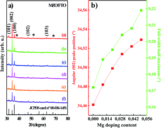 |
| | Fig. 3 (a) X-ray diffraction patterns of MZO thin films for various Mg concentrations: (a) 0, (b) 0.8, (c) 1.6, (d) 2.4, (e) 3.3, and (f) 4 mM. The XRD peaks of the FTO substrate are marked by asterisks. (b) Mg doping content dependent angular position and full-width-half-maximum (FWHM) of (002) peaks variation in MZO structures. | |
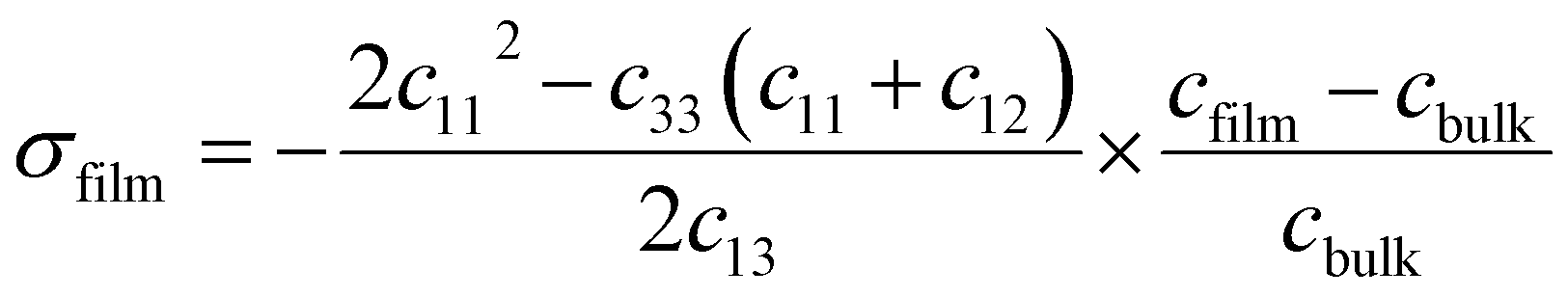
The strain can be estimated as ε = [cfilm − cbulk/cbulk] in the c-axis direction, i.e., perpendicular to the substrate was measured by XRD.39 Where cfilm and cbulk are the c-axis lattice constant of the MZO thin film and free-strain ZnO bulk crystal, respectively. To derive the film stress (σfilm) value, the following expression was used, which is valid for the hexagonal wurtzite structure:39
| |
 | (7) |
where
cij is the elastic constants of single-crystalline ZnO;
c11 = 208.8,
c33 = 213.8,
c12 = 119.7,
c13 = 104.2 Gpa. This yields the following numerical formula for the stress derived from XRD:
σfilm = −233
ε (Gpa). The calculated data were listed in
Table 2. The negative sign in biaxial stress (
σ) values indicated that all the MZO films were in a state of compressive stress. The calculated
σ values showed a tendency to decrease by increasing the Mg dopant content. The decrement of compressive stress correlates well with the decreasing tendency of the strain values as shown in
Table 2. This is evident and reported earlier also in the literature for Mg doped ZnO films owing to the difference in ionic radius and their doping content as well.
40
Table 2 Displays effect of the Mg doping concentration on microstructural properties of ZnO thin films as estimated from XRD results
| Samples |
ε |
σ (GPa) |
D (nm) |
δ (line per nm) |
N (nm−2) |
| MZO0 |
−1.152 × 10⁻³ |
−0.268 |
92.952 |
1.157 × 10⁻⁴ |
3.375 × 10⁻⁴ |
| MZO1 |
−1.728 × 10⁻³ |
−0.402 |
87.684 |
1.300 × 10⁻⁴ |
4.450 × 10⁻⁴ |
| MZO2 |
−2.112 × 10⁻³ |
−0.492 |
82.111 |
1.483 × 10⁻⁴ |
5.419 × 10⁻⁴ |
| MZO3 |
−2.689 × 10⁻³ |
−0.626 |
78.517 |
1.622 × 10⁻⁴ |
6.197 × 10⁻⁴ |
| MZO4 |
−3.073 × 10⁻³ |
−0.716 |
77.031 |
1.685 × 10⁻⁴ |
6.563 × 10⁻⁴ |
| MZO5 |
−3.457 × 10⁻³ |
−0.805 |
73.053 |
1.873 × 10⁻⁴ |
7.964 × 10⁻⁴ |
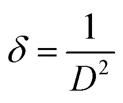
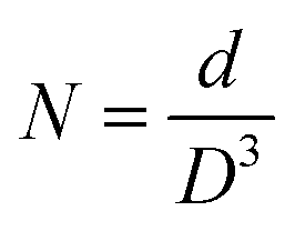
The crystallites size, the dislocation density and the crystallites number per unit volume of the crystal were calculated using the following equations:41,42
| |
 | (8) |
| |
 | (9) |
| |
 | (10) |
where
D is the average crystallites size (nm),
k is shape factor (
k = 0.89),
λ is the wavelength of the incident radiation used,
β represents the full-width-half-maximum (FWHM) value of the XRD peak (rad),
θ is the Bragg diffraction angle (rad),
δ is the dislocation density,
N denotes the number of crystallites per unit volume and
d is the films thickness. The estimated values are summarized in
Table 2. The calculated results showed that the crystallites size values were gradually decreased with increasing Mg dopant content within MZO films from 0 to 4 mM. This fact is well supported by the observed decreasing tendency of FWHM discussed before. Such behavior was believed to be attributed to the increase in deposition rate with the increase of the Mg doping. The crystallites size can be controlled simply by varying the concentration dopant. Effectively, a higher dopant level generates a greater amount of nucleation centers along with lattice defects, and induces, therefore, a reduction of the crystallite size of the prepared thin films. Results indicated also the increase of the dislocation density with the increase of Mg doping, which reveals the increase of lattice defects along the grain boundaries in MZO thin films. The fact that the
N exhibited an increasing trend with the increase of Mg doping was believed to be caused by the increase of the nucleation density and growth rate of MZO thin films with the contribution of Mg doping. This argument fitted well the results obtained from the voltammetry analysis (
Fig. 1a).
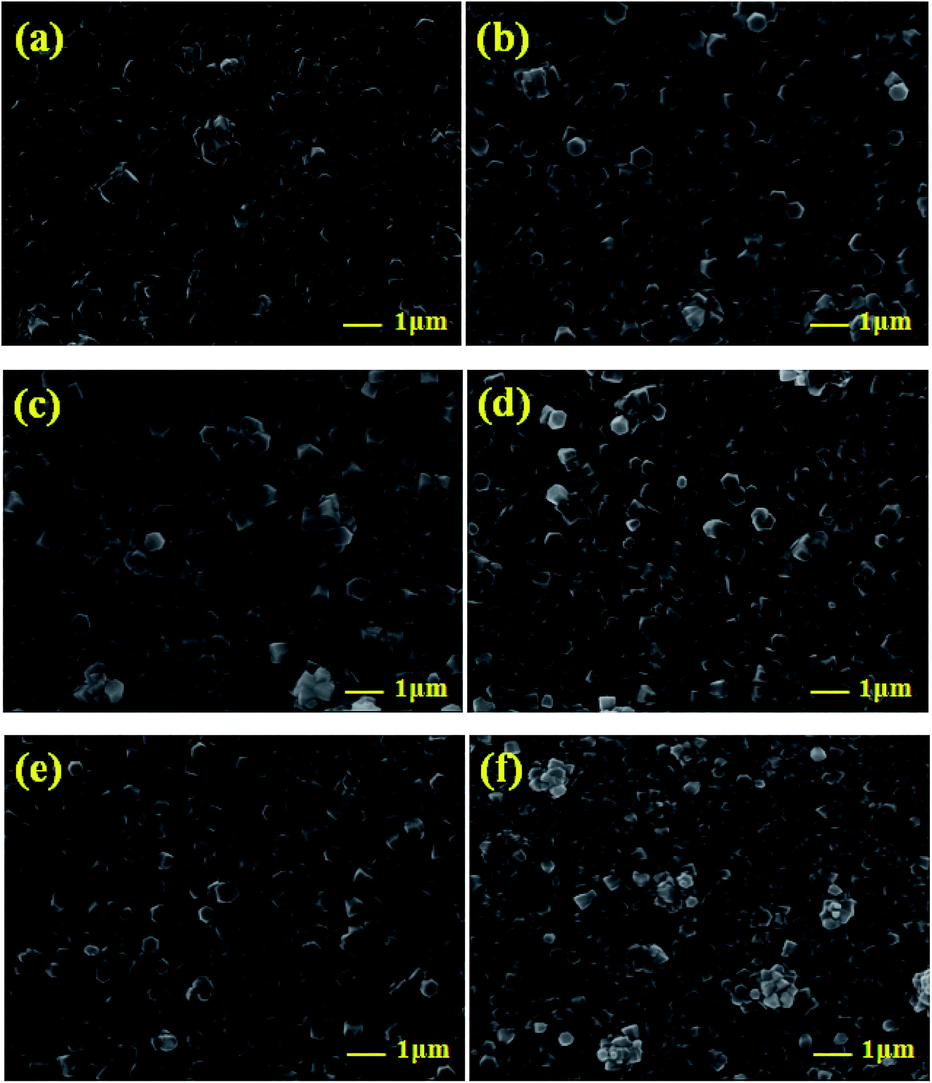
The influence of the Mg doping on the morphological features of the electrodeposited MZO thin films was further examined by scanning electron microscopy (SEM) and atomic force microscopy (AFM). Fig. 4a–f illustrated typical plane-view SEM micrographs of MZO thin films coated FTO substrate with Mg at different concentrations. It is evident that the electrodeposited films exhibited uniformly distributed grains covering the whole surface of the substrate with hexagonal features. This suggested the preferential growth of the MZO layers along the [0001] c-axis direction, perpendicular to the substrate. No obvious defects, such as cracks and empty-holes were observed on the surface of the films, revealing the high quality of our electrodeposited samples. Notably, by the inclusion of the magnesium doping, more compact, flat and smoother films were obtained. Fig. 5 shows a sequence of tapping mode AFM images with a scan area of 10 μm × 10 μm for the electrodeposited MZO thin films onto FTO substrate obtained at different Mg doping concentrations. The root mean square (RMS) of the average surface roughness of the samples defined as the standard deviation of the surface height profile from the mean height was shown in the inset of Fig. 5. As can be seen from the AFM images, the surface of the MZO thin films displayed a granular nature with a decrease in grains size at high Mg doping level. These observations were conformed with the variation of the RMS surface roughness which was decreased from 73.154 nm for undoped ZnO film to 65.484 and 21.221 nm for Mg-doped ZnO films with the increase of Mg doping content from 1 to 5%, respectively. Such behavior revealed that Mg dopants might act as surfactants. The presence of Mg in ZnO thin films modifies the diffusion rate of zinc (Zn) and oxygen (O) at the surface substrate during the deposition process. Similar observations have been reported by Mass et al.43 for doped n-type ZnO thin films. The decrease in the RMS roughness brought in by Mg doping is worth noting since it may increase the conducting paths and decrease the electrical resistivity of MZO thin films.
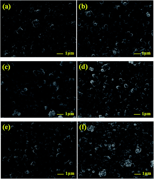 |
| | Fig. 4 FE-SEM images of ZnO thin films doped and undoped with Mg: (a) 0, (b) 0.8, (c) 1.6, (d) 2.4, (e) 3.3, and (f) 4 mM. | |
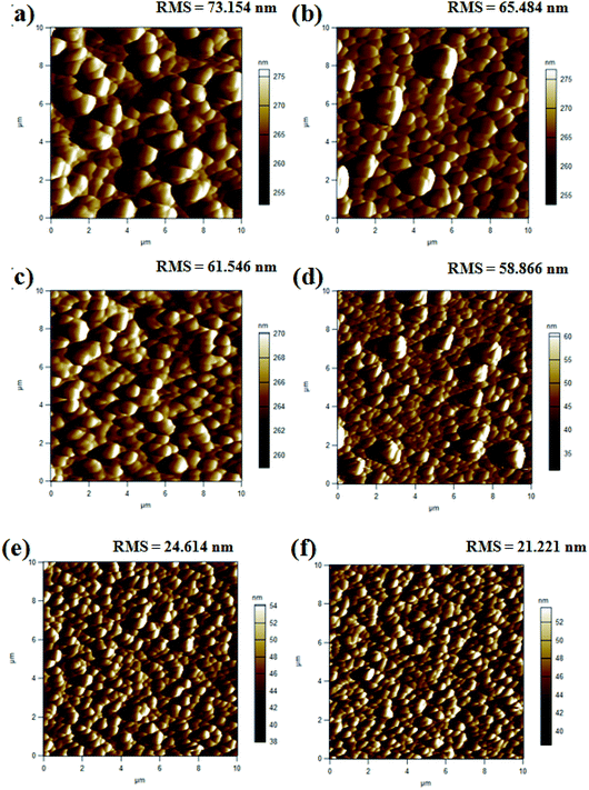 |
| | Fig. 5 Tapping mode 2D AFM images of MZO thin films for various Mg concentrations: (a) 0, (b) 0.8, (c) 1.6, (d) 2.4, (e) 3.3, and (f) 4 mM. The root mean square (RMS) of average surface roughness was shown in the inset. | |
Fig. 6a shows the optical transmittance spectra in the range of 200 to 800 nm for the MZO films at different Mg concentrations. The first derivation of the optical transmittance (dT/dλ) in which the position of the maximum absorption peaks corresponds to the absorption band edge was showed in Fig. 6b. The undoped ZnO thin film exhibited average optical transparency of 70% in the visible spectral region. However, for Mg-doped ZnO thin films the average optical transparency increases about a 15% compared to the undoped ZnO thin film. The transmittance spectra exhibited an inherent absorption band edge at 372 nm for the undoped ZnO film as extracted from the inset of Fig. 6a. The increase of the optical transmittance in the visible spectral range near to the band edge for the Mg-doped ZnO sample suggests that the deposited Mg-free film is slightly sub-stoichiometric.44,45 This is in good agreement with a decrease of the {101} XRD reflections in the case of films containing a high amount of Mg dopants as illustrated in the XRD measurements. The (101) diffraction peak has been found to appear in the case of sub-stoichiometric films as demonstrated by Horwat and Billard.46 The high optical transparency brought in by the contribution of the Mg doping approach probes the potentiality of the fabricated Mg-doped ZnO thin films to act as efficient TCOs material.47 The transmittance spectra exhibited an inherent absorption band edge at 372 nm for the Mg-free thin film as extracted from the inset of Fig. 6a. The effect of the contribution of the Mg doping on the absorption band edge of the MZO films resulted in a gradual shift towards shorter wavelengths side. The absorption band edge was shifted from 370 to 362 eV as the Mg doping content within MZO films was altered from 1 to 5%, respectively. This blue-shift indicated the electronic structure bandgap engineering of the MZO films and further reaffirmed that Mg impurities had incorporated into the ZnO host structure. Fig. 6c depicted the UV-Vis absorption spectra of MZO thin films deposited at different Mg doping. From these figures, all the samples showed a single shoulder onset reaffirming the absence of secondary phases in the electrodeposited samples.48 The absence of sharpness in the optical absorbance feature was due to the direct forbidden gap nature of the deposits. From Fig. 6c, it can be seen that both of the undoped and Mg-doped ZnO thin films exhibited a strong absorption across the ultraviolet spectral region. Effectively, the intensity and the threshold of the optical absorption bands of the Mg-doped ZnO thin films were increased gradually at the ultraviolet spectral region with the increase of the amount of Mg dopants. Such behavior suggested that the Mg doping could be an effective way to improve the UV light-harvesting ability of the MZO thin films based optoelectronic devices.
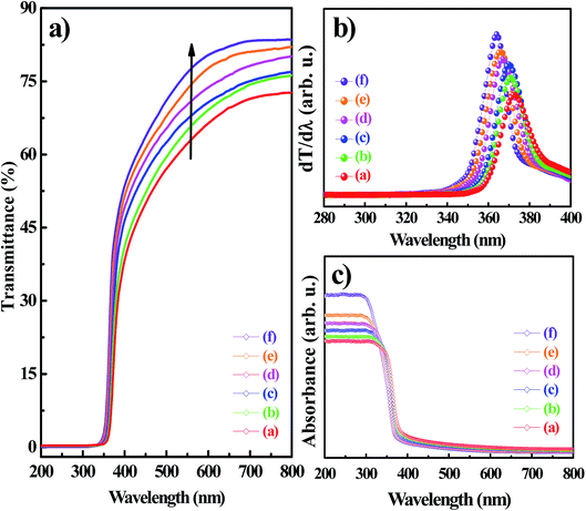 |
| | Fig. 6 (a) Optical transmittance spectra of ZnO thin films doped and undoped with Mg: (a) 0, (b) 0.8, (c) 1.6, (d) 2.4, (e) 3.3, and (f) 4 mM. (b) The first derivation of the optical transmittance (dT/dλ) vs. wavelength (λ). (c) Optical absorption spectra of MZO thin films for various Mg concentrations. | |
In order to determine the effect of Mg doping concentration on the absorption edge, the optical band gap energies of the undoped and Mg-doped ZnO thin films were determined through the plot of the Tauc relation described in eqn (11),49 where hv, A, and Eg are the incident photon energy, material-dependent constant, and bandgap energy, respectively.
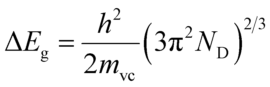
Fig. 7 showed (αhv)2 vs. hv plots of the MZO thin films at different Mg concentrations. The optical band gap energies of MZO thin films can be obtained by extrapolating the linear region near the onset in the Tauc's plot.49 It is well demonstrated that the optical band gap changes in accordance with an increase in the Mg doping concentrations. In fact, the intercepts 3.307, 3.345, 3.362, 3.381, 3.402 and 3.417 eV corresponded to MZO thin films with Mg concentrations of 0, 1, 2, 3, 4 and 5%, respectively. The broadening or blue shift of the Eg was most likely caused by the so-called Burstein Moss effect resulted from the increase of the charges carrier density introduced by increasing the Mg doping.50–52 The high charges carrier density filled the lowest states at the bottom of the conduction band. Since the Pauli principle prevents the double occupancy of states and the optical transitions are vertical, the electrons in the valence band require extra-energy to be excited to higher-energy states in the conduction band. Therefore, the optical bandgap energy of ZnO films broadened after Mg doping.50 According to this Burstein–Moss effect, the bandgap energy would increase linearly with the increase of the charges carrier density the power of 2/3:29
| |
 | (12) |
where Δ
Eg is the bandgap energy broadening given as
Eg (Mg-free film) −
Eg (Mg-containing film),
h is the Plank's constant,
mvc is the reduced effective mass and
ND is the charges (donors) density. The linear dependence of Δ
Eg with (
ND)
2/3 was depicted in
Fig. 7b.
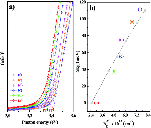 |
| | Fig. 7 (a) (αhν)2 vs. hν plots of MZO thin films for various Mg concentrations: (a) 0, (b) 0.8, (c) 1.6, (d) 2.4, (e) 3.3, and (f) 4 mM. (b) Representation of the bandgap shift (ΔEg) versus the carrier density (ND) at the 2/3 power of MZO thin films for various Mg concentrations. | |
Electrical properties play a key role in optoelectronic applications and it is well known that electrical characteristics are strongly influenced by doping content.47 As a result, the devices composed of Au/MZO/FTO thin films with Mg at different concentrations are fabricated in order to determine the influence of Mg doping on the electrical properties of the electrodeposited ZnO thin films. Gold (Au) contacts were deposited as a front contact by DC reactive sputtering on top of MZO-coated FTO through a mask having 2 mm2 openings. Fig. 8 shows dark current–voltage (I–V) characteristics of MZO/FTO devices with cell area equal to 0.32 cm2 under room temperature. The inset illustrated the schematic representation of the fabricated Au/MZO/FTO samples. Experimental results show good ohmic contacts between Au metal and MZO thin films and the proportional increase in the current density to the supplied voltage for the films under both forward and reverse bias conditions. I–V measurements indicate also the increase in the slope of the I–V curves of MZO/FTO contacts due to the increase of Mg doping content in ZnO lattice. Such a behavior was possibly attributed to occupancy of Mg ion on the Zn site acting as a donor that can enhance the density of free charge carriers and the electrical conductivity of the films.51 This argument fits well with the results obtained from the Mott–Schottky measurement demonstrating the increase of the density of the free charge carriers of MZO samples with the inclusion of magnesium doping approach (Table 1 and Fig. 2). The consistency in the electrical analysis demonstrated the formation of the desired products.
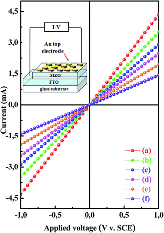 |
| | Fig. 8 Dark current density–voltage (I–V) characteristics of Au/MZO/FTO thin film devices at different Mg doping: (a) 0, (b) 0.8, (c) 1.6, (d) 2.4, (e) 3.3, and (f) 4 mM. The inset showed the schematic illustration of Au/MZO/FTO devices structure with top contact. | |
4. Conclusions
The electronics, structural, morphological, optical and electrical properties of undoped and Mg-doped ZnO films grown by electrodeposition method on FTO glass substrates have been investigated. Mg doping greatly enhanced the charges carrier density while reduced the flat band potential and Fermi level energy of MZO films. XRD patterns showed the growth of MZO films along the (002) plane with a hexagonal wurtzite structure. The average crystallite sizes of the MZO films were found to be in the range of 73 to 92 nm. The surface morphology and topography of the films showed hexagonal-shaped particles, uniformly distributed over the surface. Furthermore, increasing Mg doping concentration results in finer microstructures, and improves compactness and surface flatness of the MZO thin films. The transmittance of the deposits was found to be very high, reaching 85% in the visible region of the solar spectrum. The bandgap energy of MZO films increased with increasing Mg content in ZnO structure. The current–voltage characteristics of the Mg-doped ZnO based devices showed a significant improvement as compared to the undoped reference device, probing the Mg doping role in enhancing the quality and the optoelectrical properties of MZO TCO material.
Conflicts of interest
There are no conflicts to declare.
Acknowledgements
It is included in the PRFU of Ferhat Abbas-Sétif 1 University No. B00L01UN190120200001. This work was funded under the Algerian General Directorate of Scientific Research and Technological Development (DGRSDT)/MESRS.
References
- H. Ohta and H. Hosono, Transparent oxide optoelectronics, Mater. Today, 2004, 7(6), 42–51 CrossRef CAS.
- Y. Hu, X. Diao, C. Wang, W. Hao and T. Wang, Effects of heat treatment on properties of ITO films prepared by rf magnetron sputtering, Vacuum, 2004, 75(2), 183–188 CrossRef CAS.
- S. Sharma, S. Shriwastava, S. Kumar, K. Bhatt and C. C. Tripathi, Alternative transparent conducting electrode materials for flexible optoelectronic devices, Opto-Electron. Rev., 2018, 26(3), 223–235 CrossRef.
- B. Efafi, S. S. Mousavi, M. H. M. Ara, B. Ghafari and H. R. Mazandarani, A method for optimizing the electrical conductivity of Al:ZnO TCO films, Mater. Lett., 2017, 195, 52–54 CrossRef CAS.
- J. Wang, R. Chen, L. Xiang and S. Komarneni, Synthesis, properties and applications of ZnO nanomaterials with oxygen vacancies: a review, Ceram. Int., 2018, 44(7), 7357–7377 CrossRef CAS.
- V. Consonni, J. Briscoe, E. Kärber, X. Li and T. Cossuet, ZnO nanowires for solar cells: a comprehensive review, Nanotechnology, 2019, 30, 362001 CrossRef CAS.
- Z. K. Heiba and M. B. Mohamed, Effect of annealed and Mg-doped nano ZnO on physical properties of PVA, J. Mol. Struct., 2019, 1181, 507–517 CrossRef CAS.
- Ş. Ş. Türkyılmaz, N. Güy and M. Özacar, Photocatalytic efficiencies of Ni, Mn, Fe and Ag doped ZnO nanostructures synthesized by hydrothermal method: the synergistic/antagonistic effect between ZnO and metals, J. Photochem. Photobiol., A, 2017, 341, 39–50 CrossRef.
- K. Joshi, M. Rawat, S. K. Gautam, R. G. Singh, R. C. Ramola and F. Singh, Band gap widening and narrowing in Cu-doped ZnO thin films, J. Alloys Compd., 2016, 680, 252–258 CrossRef CAS.
- C. Lung, M. Toma, M. Pop, D. Marconi and A. Pop, Characterization of the structural and optical properties of ZnO thin films doped with Ga, Al and (Al+Ga), J. Alloys Compd., 2017, 725, 1238–1243 CrossRef CAS.
- P. Kumar, H. K. Malik, A. Ghosh, R. Thangavel and K. Asokan, Bandgap tuning in highly c-axis oriented Zn1-xMgxO thin films, Appl. Phys. Lett., 2013, 102(22), 221903 CrossRef.
- R. Kavitha and V. Jayaram, Band-Gap Engineering in ZnO-MgO Films Prepared by Combustion Flame Pyrolysis of Solution Precursors, J. Electron. Mater., 2017, 36(10), 1326–1332 CrossRef.
- S. Ren, H. Wang, Y. Li, H. Li, R. He, L. Wu, W. Li, J. Zhang, W. Wang and L. Feng, Rapid thermal annealing on ZnMgO window layer for improved performance of CdTe solar cells, Sol. Energy Mater. Sol. Cells, 2018, 187, 97–103 CrossRef CAS.
- Y. Kuwahata and T. Minemoto, Impact of Zn1-xMgxO:Al transparent electrode for buffer-less Cu(In, Ga)Se2 solar cells, Renewable Energy, 2014, 65, 113–116 CrossRef CAS.
- K. Huang, Z. Tang, L. Zhang, J. Yu, J. Lv, X. Liu and F. Liu, Preparation and characterization of Mg-doped ZnO thin films by sol–gel method, Appl. Surf. Sci., 2012, 258(8), 3710–3713 CrossRef CAS.
- T. Gruber, C. Kirchner, R. Kling, F. Reuss and A. Waag, ZnMgO epilayers and ZnO-ZnMgO quantum wells for optoelectronic applications in the blue and UV spectral region, Appl. Phys. Lett., 2004, 84(26), 5359–5361 CrossRef CAS.
- M. Arshad, M. Meenhaz Ansari, A. S. Ahmed, P. Tripathi, S. S. Z. Ashraf, A. H. Naqvi and A. Azam, Band gap engineering and enhanced photoluminescence of Mg doped ZnO nanoparticles synthesized by wet chemical route, J. Lumin., 2015, 161, 275–280 CrossRef CAS.
- H.-C. Chiu, H.-C. Wang, C.-K. Lin, C.-W. Chiu, J. S. Fu, K.-P. Hsueh and F.-T. Chien, Low Frequency Noise Analysis of Top-Gate MgZnO Thin-Film Transistor with High-κ ZrO2 Gate Insulator, Electrochem. Solid-State Lett., 2011, 14(9), H385 CrossRef CAS.
- K. Karthick and K. Vijayalakshmi, Influence of Mg doping on the properties of ZnO films prepared on c-cut sapphire by sputtering, Superlattices Microstruct., 2014, 67, 172–180 CrossRef CAS.
- M. N. H. Mia, M. F. Pervez, M. K. Hossain, M. Reefaz Rahman, M. J. Uddin, M. A. Al Mashud, H. K. Ghosh and M. Hoq, Influence of Mg content on tailoring optical bandgap of Mg-doped ZnO thin film prepared by sol-gel method, Results Phys., 2017, 7, 2683–2691 CrossRef.
- L. Mentar, O. Baka, M. R. Khelladi, A. Azizi, S. Velumani, G. Schmerber and A. Dinia, Effect of nitrate concentration on the electrochemical growth and properties of ZnO nanostructures, J. Mater. Sci.: Mater. Electron., 2015, 26, 1217–1224 CrossRef CAS.
- O. Baka, A. Azizi, S. Velumani, G. Schmerber and A. Dinia, Effect of doping concentration on the electrodeposition and properties of Al doped ZnO, J. Mater. Sci.: Mater. Electron., 2014, 25, 1761–1769 CrossRef CAS.
- O. Baka, M. R. Khelladi, L. Mentar and A. Azizi, Growth and properties of electrodeposited transparent Al-doped ZnO nanostructures, J. Korean Phys. Soc., 2015, 67, L2011–L2014 CrossRef.
- J. K. Liang, H. L. Su, C. L. Kuo, S. P. Kao, J. W. Cui, Y. C. Wu and J. C. A. Huang, Structural, Optical and Electrical Properties of Electrodeposited Sb-Doped ZnO Nanorod Arrays, Electrochim. Acta, 2014, 125, 124–132 CrossRef CAS.
- T. Yoshida, D. Komatsu, N. Shimokawa and H. Minoura, Mechanism of cathodic electrodeposition of zinc oxide thin films from aqueous zinc nitrate baths, Thin Solid Films, 2004, 451–452, 166–169 CrossRef CAS.
- M. C. Figueiredo, D. Hiltrop, R. Sundararaman, K. A. Schwarz and M. T. M. Koper, Absence of diffuse double layer effect on the vibrational properties and oxidation of chemisorbed carbon monoxide on a Pt(111) electrode, Electrochim. Acta, 2018, 281, 127–132 CrossRef CAS.
- L. C.-K. Liau and J.-L. Jhan, Investigation of Rapid Thermal Annealing on Cu2O Properties and n-p Cu2O Homojunction Performance by Electrochemical Deposition Processing, J. Electrochem. Soc., 2016, 163(14), D787–D793 CrossRef CAS.
- H.-Y. Liu, H. Kong, X.-M. Ma and W.-Z. Shi, Microstructure and electrical properties of ZnO-based varistors prepared by high-energy ball milling, J. Mater. Sci., 2007, 42(8), 2637–2642 CrossRef CAS.
- Q. Li, X. Ma, H. Liu, Z. Chen, H. Chen and S. Chu, Self-Organized Growth of Two-Dimensional GaTe Nanosheet on ZnO Nanowires for Heterojunctional Water Splitting Applications, ACS Appl. Mater. Interfaces, 2017, 9(22), 18836–18844 CrossRef CAS.
- D. Kang, D. Lee and K.-S. Choi, Electrochemical Synthesis of Highly Oriented, Transparent, and Pinhole-Free ZnO and Al-Doped ZnO Films and Their Use in Heterojunction Solar Cells, Langmuir, 2016, 32(41), 10459–10466 CrossRef CAS.
- A. C. Aragonès, A. Palacios-Padrós, F. Caballero-Briones and F. Sanz, Study and improvement of aluminium doped ZnO thin films: limits and advantages, Electrochim. Acta, 2013, 109, 117–124 CrossRef.
- F. K. Shan, G. X. Liu, W. J. Lee and B. C. Shin, Stokes shift, blue shift and red shift of ZnO-based thin films deposited by pulsed-laser deposition, J. Cryst. Growth, 2006, 291(2), 328–333 CrossRef CAS.
- Z. J. Othman, A. Matoussi, F. Fabbri, F. Rossi and G. Salviati, Optical and structural properties of Zn1-xMgxO ceramic materials, Appl. Phys. A: Mater. Sci. Process., 2014, 116(3), 1501–1509 CrossRef CAS.
- I. V. Maznichenko, A. Ernst, M. Bouhassoune, J. Henk, M. Däne, M. Lüders, P. Bruno, W. Hergert, I. Mertig, Z. Szotek and W. M. Temmerman, Structural phase transitions and fundamental band gaps of MgxZn1-xO alloys from first principles, Phys. Rev. B, 2009, 80, 144101 CrossRef.
- R. Dutta and N. Mandal, Mg doping in wurtzite ZnO coupled with native point defects: a mechanism for enhanced n-type conductivity and photoluminescence, Appl. Phys. Lett., 2012, 101(4), 042106 CrossRef.
- C. M. McShane and K.-S. Choi, Junction studies on electrochemically fabricated p–n Cu2O homojunction solar cells for efficiency enhancement, Phys. Chem. Chem. Phys., 2012, 14(17), 6112 RSC.
- K. Pradeev raj., K. Sadaiyandi, A. Kennedy, S. Sagadevan, Z. Z. Chowdhury, M. R. B. Johan, F. A. Aziz, R. F. Rafique, T. Selvi and R. Rathinabala, Influence of Mg Doping on ZnO Nanoparticles for Enhanced Photocatalytic Evaluation and Antibacterial Analysis, Nanoscale Res. Lett., 2018, 13(1), 229 CrossRef CAS.
- M. Sharma and P. Jeevanandam, Magnesium doping in hierarchical ZnO nanostructures and studies on optical properties, Superlattices Microstruct., 2012, 52(6), 1083–1092 CrossRef CAS.
- R. Hong, J. Huang, H. He, Z. Fan and J. Shao, Influence of different post-treatments on the structure and optical properties of zinc oxide thin films, Appl. Surf. Sci., 2005, 242(3–4), 346–352 CrossRef CAS.
- S. Suwanboon and P. Amornpitoksuk, Preparation of Mg-doped ZnO nanoparticles by mechanical milling and their optical properties, Procedia Eng., 2012, 32, 821–826 CrossRef CAS.
- R. Mariappan, M. Ragavendar and V. Ponnuswamy, Growth and characterization of chemical bath deposited Cd1-xZnxS thin films, J. Alloys Compd., 2011, 509(27), 7337–7343 CrossRef CAS.
- Z. N. Kayani, B. Zulfiqar, S. Riaz and S. Naseem, Influence of Al percentage on the magnetic, optical, and structural properties of Al-doped CoZnO thin films, J. Aust. Ceram. Soc., 2018, 55, 479–487 CrossRef.
- J. Mass, P. Bhattacharya and R. Katiyar, Effect of high substrate temperature on Al-doped ZnO thin films grown by pulsed laser deposition, Mater. Sci. Eng., B, 2003, 103(1), 9–15 CrossRef.
- M. Mickan, U. Helmersson, H. Rinnert, J. Ghanbaja, D. Muller and D. Horwat, Room temperature deposition of homogeneous, highly transparent and conductive Al-doped ZnO films by reactive high-power impulse magnetron sputtering, Sol. Energy Mater. Sol. Cells, 2016, 157, 742–749 CrossRef CAS.
- M. Jullien, D. Horwat, F. Manzeh, R. Escobar Galindo, P. Bauer, J. F. Pierson and J. L. Endrino, Influence of the nanoscale structural features on the properties and electronic structure of Al-doped ZnO thin films: an X-ray absorption study, Sol. Energy Mater. Sol. Cells, 2011, 95(8), 2341–2346 CrossRef CAS.
- D. Horwat and A. Billard, Effects of substrate position and oxygen gas flow rate on the properties of ZnO: Al films prepared by reactive co-sputtering, Thin Solid Films, 2007, 515(13), 5444–5448 CrossRef CAS.
- N. Jabena Begum and K. Ravichandran, Effect of source material on the transparent conducting properties of sprayed ZnO:Al thin films for solar cell applications, J. Phys. Chem. Solids, 2013, 74(6), 841–848 CrossRef CAS.
- R. Kara, R. Siab and A. Azizi, Effect of i-ZnO seed layer on the properties of electrodeposited p-Cu2O/n-ZnO/FTO heterojunction thin films, Mater. Res. Express, 2019, 126402 CrossRef CAS.
- J. Tauc, Optical Properties of Solids, ed. Abeles, North Holland, Amsterdam, 1972 Search PubMed.
- E. Burstein, Anomalous Optical Absorption Limit in InSb, Phys. Rev., 1954, 93(3), 632–633 CrossRef CAS.
- S. S. Cetin, I. Uslu, A. Aytimur and S. Ozcelik, Characterization of Mg doped ZnO nanocrystallites prepared via electrospinning, Ceram. Int., 2012, 38(5), 4201–4208 CrossRef CAS.
- R. Kara, H. Lahmar, L. Mentar, R. Siab, F. Kadirgan and A. Azizi, Electrochemical growth and characterization of Cu2O:Na/ZnO heterojunctions for solar cells applications, J. Alloys Compd., 2019, 152748 Search PubMed.
|
| This journal is © The Royal Society of Chemistry 2020 |
Click here to see how this site uses Cookies. View our privacy policy here. 
 Open Access Article
 This Open Access Article is licensed under a Creative Commons Attribution-Non Commercial 3.0 Unported Licence
 ab,
L. Mentar
ab,
L. Mentar