 Open Access Article
Dissipation enhancement effect from titania semiconductor modulation of graphene-based electromagnetic absorbing composites†
Yi Lixi * and
Wu Jinwu
School of Aircraft Engineering, Nanchang Hangkong University, Nanchang 330063, China. E-mail: yilixi@nchu.edu.cn
First published on 17th December 2020
Abstract
A scheme of semiconductor modulation of electromagnetic (EM) absorbing materials is proposed. Homogeneous composites as ideal media are obtained by uniformly mixing fillers using supercritical fluid (SCF) processing. Based on the ideal media, titania modulation design prediction of surface shield materials is confirmed for the EM composites of graphene nanosheets and manganese oxides. A low ratio of titania between 10 percent and 50 percent gives rise to dissipation enhancement in the absorbers. Simulation of the involved cases displays the EM fields in the composite absorbers, demonstrating EM energy loss in the absorbers. Frequency modulation using titania improves the electromagnetic compatibility (EMC) of the absorbing materials in the X and Ku bands. Rapid exfoliation and full premixing of the components by SCF contribute to the modulation scheme confirmation with uniform media. Semiconductor titania modulation of EM-absorbing composites is effective.
1. Introduction
As is well known, absorbing materials are important supports for modern equipment, including civilian facilities, military products, and even defensive anti-detection of flight. Shielding design in aircraft stealth technology is of tactical significance. The overall absorbing effects of surface structural materials are influenced by their macroscopic configuration and the matrix material type.1,2 A similar matrix has little influence on the absorbing effect. Macro configuration exhibits good effects through structural design. However, the absorbing effect discussed in this study is considered to be a surface composite material property. Electromagnetic (EM) wave propagation in the matrix is elongated. The interactions between EM waves and filler materials during the conduction process will become full via elongated paths. Graphene nanosheets (GNS) are conductive materials. GNS are two-dimensional materials, providing natural conditions to form a large number of sandwich microcavity structures. GNS have large surfaces and high specific surface areas. The cavities formed by the nanosheets provide structures for reciprocating the absorption of inner resident wave. Thus, graphene-based nanocomposites have superior absorbing properties in microstructures.1,3 However, in general nanomaterial filling methods, nanomaterial microstructures are often not particularly designed in advance. It is difficult to fabricate composites that possess significant performance improvement. Hence, graphene-based composites are a good choice to obtain high performance. The properties of filler materials are important aspects of EM wave dissipation resulting from the interaction between waves and materials.Electric loss-type absorbers mainly include dielectric or conductive materials. Magnetic loss-type composites mainly include magnetic materials. Research exists on the optimization of the microwave-absorbing properties of conductive carbon nanotubes and magnetic oxide composite materials.4 In addition to conductive and magnetic materials, whether the additional contents interacting with EM waves play important roles in the absorbing performance is worth examining. This work discusses the effects of the interaction between EM waves and material properties for scientific design research. A semiconductor modulation scheme using exfoliated GNS and manganese oxide composites is investigated to confirm the effects of the titania semiconductor. The interaction mechanism between the EM waves and micro-nano filler materials is clarified.
However, homogeneity of an ideal absorber medium is a prerequisite to determine the properties of a sample for scheme confirmation, especially for multi-components. Uniformity can enable the collected parameters to characterize the scheme samples, exactly reflecting the properties of the medium.5,6 Stirring during the composite formation process contributes to uniformity of particle groups on a relatively macro level. Hence, to achieve uniformity of absorber media, fully premixed filler components are an important aspect of multi-component fillers. In the engineering area, some basic experimental parameters are necessary as initial settings for simulation. A feasible method to obtain satisfactory homogeneity of a sample before production is significant. Reliable parameters are important for advanced simulation. Therefore, a reliable production method to obtain ideal samples is crucial.
SCFs have the properties of high diffusivity, low surface tension and fast mass transfer.7 Their mixing mechanisms include convective mixing, diffusive mixing, and shear mixing.8,9 SCF characteristics provide conditions for promoting uniformity resulting from premixing of small solid particles. Premixing uniformity contributes to the multi-component homogeneity dispersion state of composites as ideal media. SCF exfoliation has gradually become a mature process to prepare two-dimensional materials, including the preparation of GNS,10,11 two-dimensional nanomaterials,12,13 and other low-dimensional nanomaterials.14,15 Harsh reaction conditions can overcome the difficulty of mixing components with micro-nano sizes to assist the preparation of wave-absorbing fillers.11 Fast exfoliation by the SCF method enables convenient adjustment of the component ratios. In this work, supercritical N,N-dimethylformamide exfoliation is used to prepare GNS, magnetic manganese oxide and semiconductor titania nanomaterials. Based on the SCF-processed fillers, composite materials, and theoretical analysis, introduction of semiconductors into the absorbers is carried out to study its modulation effect on the absorbing properties. Molded samples of filled composites are prepared using a polymer matrix with a casting method. The consistency of the simulation using the parameters of ideal media obtained by supercritical fluid-assisted mixing demonstrates the feasibility of SCF processing for ideal media. This work provides necessary theoretical analysis methods and simulation evaluation for the development of semiconductor modulation EM wave-absorbing materials as well as necessary experimental method support.
2. Experimental
2.1. Reagents
Natural graphite and N,N-dimethylformamide were purchased from Sinopharm Chemical Reagent Co., Ltd, China. The epoxy resin, curing agent, and silicon oil are industrial products.2.2. Preparation and formation of materials
Graphite was purchased from commercial sources; layered titanate and manganese oxides were obtained by a flux growth method in the laboratory. Literature procedures were used to obtain layered titanate and manganese oxides, as reported previously.12,13,16 SCF exfoliation processing was utilized to obtain exfoliated products as composite fillers by following the steps in previous work.3,12,13 N,N-dimethylformamide was used as the reaction reagent. After the disposal with low sonication and vibration, the precursors were dispersed in the reagent. 10 mL of the dispersed reactants were taken into a special stainless container for processing. The mixing course with exfoliation was finished in an ice-cold water bath as soon as the fluid reached the supercritical state. Among the filler samples containing titania, their precursors were introduced by adding 10, 30 and 50 percent titanate to well-mixed 1![[thin space (1/6-em)]](https://www.rsc.org/images/entities/char_2009.gif) :
:![[thin space (1/6-em)]](https://www.rsc.org/images/entities/char_2009.gif) 1 manganese oxide and graphite. The other precursor was a mixture of 1
1 manganese oxide and graphite. The other precursor was a mixture of 1![[thin space (1/6-em)]](https://www.rsc.org/images/entities/char_2009.gif) :
:![[thin space (1/6-em)]](https://www.rsc.org/images/entities/char_2009.gif) 1 layered graphite and titanate or manganese oxide. Then, the exfoliated products, including GNS, exfoliated manganese oxides (EMO) and exfoliated titania, were mixed with the corresponding ratios. The corresponding filled composite samples were named GMT10 (graphene–manganese oxides–titania of 10 percent), GMT30 (graphene–manganese oxides–titania of 30 percent), GMT50 (graphene–manganese oxides–titania of 50 percent), GT (graphene–titania), and GM (graphene–manganese oxides), respectively. The samples with 30 percent titania were utilized in typical characterization of the exfoliated products and composites. Epoxy resin was blended with the exfoliated products in a volume ratio of 1
1 layered graphite and titanate or manganese oxide. Then, the exfoliated products, including GNS, exfoliated manganese oxides (EMO) and exfoliated titania, were mixed with the corresponding ratios. The corresponding filled composite samples were named GMT10 (graphene–manganese oxides–titania of 10 percent), GMT30 (graphene–manganese oxides–titania of 30 percent), GMT50 (graphene–manganese oxides–titania of 50 percent), GT (graphene–titania), and GM (graphene–manganese oxides), respectively. The samples with 30 percent titania were utilized in typical characterization of the exfoliated products and composites. Epoxy resin was blended with the exfoliated products in a volume ratio of 1![[thin space (1/6-em)]](https://www.rsc.org/images/entities/char_2009.gif) :
:![[thin space (1/6-em)]](https://www.rsc.org/images/entities/char_2009.gif) 1. After a curing agent was added, the mixtures were mixed uniformly again. Then, the mixtures were quickly cast into hollow cylinder molds. The molds for the formation of the composites were painted in advance with silicone oil. Molding was carried out under ambient atmosphere for one night to obtain specimens for the reflectivity measurements. The internal and external diameters of the formed specimens were respectively equal to 3.04 and 7 mm, with a thickness of 4 mm. The samples were shaped like a partial shield shell of a cable.
1. After a curing agent was added, the mixtures were mixed uniformly again. Then, the mixtures were quickly cast into hollow cylinder molds. The molds for the formation of the composites were painted in advance with silicone oil. Molding was carried out under ambient atmosphere for one night to obtain specimens for the reflectivity measurements. The internal and external diameters of the formed specimens were respectively equal to 3.04 and 7 mm, with a thickness of 4 mm. The samples were shaped like a partial shield shell of a cable.
2.3. Characterization and measurements
X-ray diffraction (XRD) was performed using a D8 Advance X-ray diffraction apparatus (Cu Kα copper radiation of λ = 0.15405 nm, 40 kV and 40 mA) to examine the material phases in the samples at steps of 2θ = 0.02°. Scanning electron microscopy (SEM) was utilized to determine the section morphologies of the cured composites by slowing down the electron beam. Exfoliated samples and cut pieces for SEM observation were sputtered with Au. Scanning electron microscopy (SEM) micrographs of each filler component before SCF treatment were obtained using a FEI SIRION 200 field-emission scanning electron microscope operated at an accelerating voltage of 5.0 kV. The other SEM images were obtained using an S-4800 (Hitachi) field-emission scanning electron microscope operated at an accelerating voltage of 15.0 kV. Infrared (IR) spectra were achieved using a Fourier transform infrared spectrometer (Nicolet 6700 FT-IR, Thermo Fisher Scientific Inc.), to discover the material modalities before and after formation. Composite samples after formation for IR spectra were obtained by repeatedly shaving small powder particles from a solidified block with mechanical tools. EM parameters were obtained according to the transmission/reflection method using a two-port Agilent network analyzer (N5224A), adapted with a 7 mm coaxial transmission line, in the frequency range from 2 to 18 GHz. Some related physical quantities were converted by software with Maxwell theory.3. Results and discussion
3.1. Mixed fillers from SCF exfoliation and composites
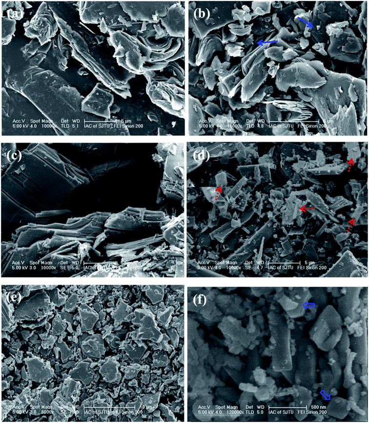
SCF can provide a harsh environment for low-dimension material processing,10,11 forming a natural fluid mixer for fast exfoliation and reaction in a one-step method.13,14 The stirring from the fluid mixer uniformly disperses the reactants. The effects of exfoliation were determined from single component exfoliation of the layered materials. The mixing effects during exfoliation can be identified from the comparison between single component exfoliation and one-step exfoliation of multi-components.SEM micrographs of each filler component, namely layered graphite, titania and manganese oxide, before and after SCF treatment are exhibited in Fig. 1. The reduced sizes due to harsh exfoliation are obvious among the three precursors in the single exfoliation cases. Fig. 1(a) and (b) show graphite and exfoliated GNS, respectively. After SCF exfoliation, the exfoliated sizes decrease to several microns or below. Fig. 1(c) is layered titanate. Fig. 1(d) is exfoliated titania. The initial sizes are 10 microns or more for graphite and layered titanate. However, from the comparison in Fig. 1(b) and (d), the small pieces of exfoliated titania even have smaller sizes than the small pieces of exfoliated GNS. The layered manganese oxides have relatively small sizes, reaching almost 10 microns, as the layered manganese oxide shown in Fig. 1(e). The exfoliated products of layered manganese oxides are reduced to nano or near-micron sizes in large quantities, as shown in Fig. 1(f). The effect of SCF exfoliation is remarkable overall.
The processing mechanism details are described in previous literature.13 The sizes of most GNS, exfoliated titania and EMO relatively decrease in sequence, agreeing with their average bond combination strengths. C–C bonds are not the strongest among these three component precursors. However, an ideal graphene sheet entirely consists of sp2-hybridized carbon atoms, possessing the strongest bond interactions in the layers. Ti has stronger bond energy with oxygen atoms than Mn.12 Hence, large quantities of the EMO have sizes of even 10–100 nanometers. This is a general scenario, but is not absolutely true for every piece of product due to the occasional exfoliation. GNS, exfoliated titania and manganese oxides have relatively reduced background contrast in sequence, as shown in Fig. 1, resulting from the electric conductivities of conductor, semiconductor, and non-conductor magnetic materials.
The SEM observation reveals the information of multi-component products from SCF exfoliation mixing by comparing with single component exfoliation. Fig. 2(a) shows a SEM observation of the mixed products of the multi-component precursors obtained from one-step exfoliation. Two-dimensional structures and small granular-shaped materials were encountered often in the course of observation. For the places labeled by block arrows in Fig. 2(a), the mixed products are almost on the nano or near-micron scales. The exfoliated products exhibit messy states, implying their fully mixed state as fillers. The mixture states are consistent with the few-component situation in previous literature reports.3,12 The shapes of the exfoliated products help distinguish some of the components. Line arrows, dotted arrows, and block arrows in the images indicate the exfoliated GNS, titania, and manganese oxides, respectively, in terms of their shape and contrast brightness. Moreover, the material phases from XRD demonstrate the coexistence of exfoliated GNS, titania and manganese oxides, as discussed in the following paragraphs. Therefore, the exfoliated products are mixed in randomly disordered states. The random positions of different components indicate well-mixed mixtures. Aggregation is a general phenomenon that occurs during exfoliation,12 especially after the exfoliation mixing process. The aggregated flakes after SCF treatment will not affect the randomly disordered relation of the different components. Provided that the aggregated flakes contain randomly mixed products, the mixing process is effective. The products present the property of uniformity. Furthermore, the products will be taken as fillers dispersed in the matrix for composite formation.
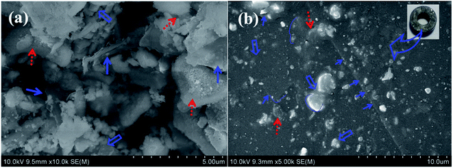 | ||
| Fig. 2 Morphologies of fillers before and after formation in composites. (a) Exfoliated fillers and (b) formed composites. | ||
One-pot preparation creates a mixture with a fully mixed state. The mixed states are expected to function as fillers. Multi-components enable electric and magnetic components to exist together at the same time, inheriting the cavity structures of GNS. These structures benefit absorption for multi-reflection. Fig. 2(b) shows a SEM image of the cross-section of the composites after formation. The fillers obviously take on dispersed states in the composites. The random dispersion phenomena are consistent with the XRD amorphous pattern analysis. The inclusion fillers have different sizes of micro or nanometers; however, their dispersion is random and separated. Background contrast of different grayscales corresponds to different kinds of materials. Embedded fillers with similar grayscales are separated. Intense aggregation no longer occurs. The embedded fillers with different grayscales are dispersive, indicating the uniformity of different filler components. The uniformity of the embedding results in homogeneity of the media, approaching ideal media as much as possible. No clefts were observed. No gaps were found between the fillers and matrix at their conjunction places in the course of the observation. Therefore, the components in the composites are fully combined. On the other hand, the components are integrated into the whole body as absorber materials. Small particulate matter leads to center points of dissipation for incident waves. The dissipation results from the eddy current in the conductor plane. Two-dimensional materials only provide working locations for eddy current. Graphene-based EM composites provide a high absorbing basis for composites with newly added contents.3
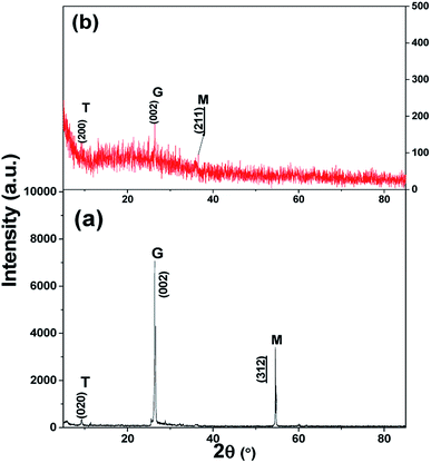
In Fig. 3, the XRD patterns display the states of the fillers before and after being embedded in the composites. The fillers from the exfoliated products possess a high crystal degree. The diffraction line shape is smooth. There are strong characteristic peaks in the pattern, as shown in Fig. 3(a). In the main diffraction range, the (020), (002) and (312) peaks, labeled T, G, and M, represent titania, graphene nanomaterials, and manganese oxides, correspondingly, as confirmed in previous work.3,12,13 From Fig. 3(a), the intensity of the graphene and manganese oxide peaks is strong. The semiconductor titania component has a relatively weak peak. Hence, the main contents are still conductive electric and magnetic components. Titania can be classified as modulation content. The X-ray diffraction peak strength demonstrates that the contents of the representative samples match the experimental manipulation ratios. Fig. 3(b) shows the XRD pattern of the smashed powder of the composite. Numerous noises exist in this pattern, indicating the amorphous state of the composite after formation. The characteristic peaks of the fillers are almost submerged in noise. The scale proportion between Fig. 3(a) and (b) is about 20![[thin space (1/6-em)]](https://www.rsc.org/images/entities/char_2009.gif) :
:![[thin space (1/6-em)]](https://www.rsc.org/images/entities/char_2009.gif) 1. In fact, the pattern of Fig. 3(b) is very planar. The amorphous states and submerged peaks indicate well-dispersed states for the fillers. Meanwhile, the combination of the fillers and matrix is suitable as an absorber.
1. In fact, the pattern of Fig. 3(b) is very planar. The amorphous states and submerged peaks indicate well-dispersed states for the fillers. Meanwhile, the combination of the fillers and matrix is suitable as an absorber.
IR spectra of the fillers before being embedded in the matrix are exhibited in Fig. 4(a). The relatively smooth line shape implies the characteristics of inorganic materials. There are several weak peaks resulting from lattice motion and the adhered functional groups. For the exfoliated fillers, small peaks near 500 cm−1 in the low wave number region are attributed to the peaks of Mn3O4. Troughs in the spectrum line shape at the position of 3432.67 cm−1 are attributed to –OH groups.17 According to the related references, this band is related to hydration water in the layered materials.13,18 The trough in the IR spectrum is broad, which results from the integrated contributions of titania, manganese oxides, and graphene oxides. However, the accuracy of the 3432.67 cm−1 peak attributed to –OH in GNS is most likely due to impurity groups in its initial state. The mixing peaks of the exfoliated products reside near 1500 cm−1.3 The peak at 501.40 cm−1 is assigned to the ν(Ti–O–Ti) stretching vibration.19 Vibrations of Ti–O give rise to the characteristic peak located at 613.25 cm−1.20 The peak band in the low wavenumber end results from the Ti–O deformation vibration between the terminated –OH and the titanium atoms on the surface as well as the O–Ti–O lattice stretching vibration.21 The characteristic peak at 925.66 cm−1 is attributed to the vibration of Ti–OH+–Ti.22 Peaks at 1025.94 and 1631.48 cm−1 belong to remnants from the SCF exfoliation and washing course due to the displacement of surface carbonate species.23
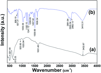 | ||
| Fig. 4 IR spectroscopy of fillers and filled composites. (a) Fillers with the addition of titania semiconductor and (b) filled composites. | ||
However, in the formed composites with fillers, many group peaks appear. Fig. 4(b) shows the IR spectrum line shape of the cured composite. Some of the characteristic peaks cover the characteristics of the filler sample in Fig. 4(a). For instance, considering the inheritance from the exfoliated products, it is consistent to assign –OH to the peak at 3415.31 cm−1 in the trough of Fig. 4(b). This trough is in the closed range of the trough in Fig. 4(a). The peak at 3415.31 cm−1 is assigned to –OH. Additionally, there are amounts of –OH in the resin.24 Hence, the trough becomes sharper in Fig. 4(b) than that for the exfoliated products in Fig. 4(a). There are small peaks in the low wave number end, as in Fig. 4(a), related to the manganese oxide and titania components. Because of the matrix covering influence, these peaks are not as obvious. The peaks at 827.31 cm−1, with a shoulder peak at 806.10 cm−1, and at 1035.58 cm−1 are related to the stretching C–O–C of the oxirane group and the stretching C–O–C of ethers, respectively. The peak located at 1182.15 cm−1 results from in-plane CH3 deformation.25 The peaks at the positions of 1247.72 cm−l and 1295.93 cm−l are attributed to the deformation of CH3 of C–(CH3)2, as achieved in hydrogenated derivatives.24 The peak at 1457.92 cm−1 implies deformation of the C–H of CH2 and CH3.24 The characteristic peaks at 1509.99 cm−1 and 1608.34 cm−1 correspond to stretching C–C and C![[double bond, length as m-dash]](https://www.rsc.org/images/entities/char_e001.gif) C of aromatic rings.24 The peaks at 2861.84, 2929.34 and 2962.13 cm−1 imply the C–H stretching of CH2 and aromatic and aliphatic CH.24,25 Distortion, double relation or triple relation of functional groups results in small peaks near these main peaks. The deformation of groups indicates that the fillers are well embedded in the resin matrix.
C of aromatic rings.24 The peaks at 2861.84, 2929.34 and 2962.13 cm−1 imply the C–H stretching of CH2 and aromatic and aliphatic CH.24,25 Distortion, double relation or triple relation of functional groups results in small peaks near these main peaks. The deformation of groups indicates that the fillers are well embedded in the resin matrix.
3.2 Simulation estimation of fields with composite EM parameters
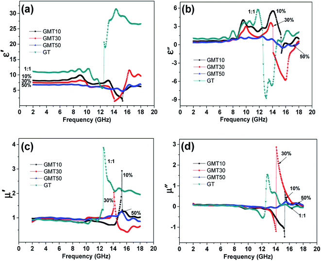
EM properties are the basis of absorbing materials. Variation of permittivity and permeability with frequency are important parameters for absorbers, reflecting the effects of different ratios of additives. These parameters are also the basis for evaluation of the absorbing effect. In the low frequency band, the real part of the parameters is reduced in the sequence of GT, GMT10, GMT30, GMT50, as the semiconductor contents increase. The variance relations are shown in Fig. 5. As accessional characterization, the change rule of the EM parameters in the unresponsive low frequency band matches the ratio change from experimental manipulation. The high permittivity for the sample with high titania and electric contents is consistent with previous research.26 However, compared with magnetic-type composites,26 the change in the parameters is inverse. After the electric components are included, the composite type becomes EM. Magnetic components demonstrate weak permittivity response. Permittivity is mainly determined by titania in references. In graphene-based composites, increased titania contents indicate relatively reduced graphene contents. Conductive graphene nanomaterials have higher permittivity compared with semiconductor titania.3,26 Therefore, the parameters are reduced as the titania content increases in graphene-based magnetic composites. Meanwhile, the parameters are relatively steady for the permittivity and permeability, as shown in Fig. 5. Large parameters corresponding to the frequency appear in the high frequency band. The permittivity has an absolute value range of 1–30 units from 10 GHz to 18 GHz, as shown in Fig. 5(a). The image part of the permittivity in Fig. 5(b) has an absolute value of no more than 9 units. The minus symbol is related to the phase of the EM waves. Negative values can result from concussion of the power amplifier during measurements. The loss of sample resulting from environmental vibration noise is another reason for the phase change of the incident electromagnetic wave. Similar negative phenomena exist in the literature,27,28 which cannot be avoided on some occasions.The GT composite filled with graphene and titania nanosheet materials has relatively large real and imaginary parts. GMT30 absorber has a large imaginary part in the EM parameters. For the permeability parameters, the GT composite also has a large real part. However, the imaginary parts of the GT composite and of the GMT10 and GMT50 composites with 10 and 5 percent semiconductors, respectively, is overwhelmed by the imaginary part of the GMT30 composite. The imaginary part of GMT30 also covered those of exfoliated GNS and EMO nanomaterials with an equal ratio in previous work.3 Consequently, the total absorbing effect is not only determined by the real part of the EM parameters; the imaginary part also plays an important role. The imaginary part affects the total absorption. The real and imaginary parts of the permeability of these composites are respectively shown in Fig. 5(c) and (d). The variation of the disordered permeability relation with the titania contents also agrees with a report in the literature.26
The excitation power supply provides energy to the composite absorbers in measurements. An electric or magnetic field is generated by EM induction. A simulation model of the circuit is needed to build it. The electric (E) field and magnetic (H) field analysis function of ANSYS software is the ideal tool for high-precision system modeling and simulation analysis.29 High frequency structure simulator software for simulation modeling of the EM field in hollow cylinder absorbers was adopted in the simulation.
Excitation conditions were applied to the coaxial hollow cylinder absorber from the end face. The simulation model had the same sizes as the absorber samples, with internal and external diameters equaling 3.04 and 7 mm as well as a thickness of 4 mm. Copper material properties were assigned to the coaxial line to contain the absorbers. Namely, the shell of the coaxial line and its axis crossing the absorber sample center are copper properties. The simulation demonstrates the propagation of EM fields in absorber media under the corresponding composite parameters with an extreme tangent loss situation. The simulation adopted a steady state simulation under the parameters at the position of strong reflection loss. The parameters for GMT10, GMT30, GMT50, and GT adopted the peak frequencies of 14.8, 14.45, 15.55 and 12.15 GHz in Table 1, respectively. The absorber density was set as the weight mass divided by the hollow cylinder volume of each sample. For other settings, the software defaults were maintained. The incident wave was also the default 1 W on the end cross section of the absorber. Simulation nephograms of these absorber samples are shown in Fig. 6 and 7, corresponding to the E field and H field, respectively.
| Recipe | Band | Freq. rang (GHz) | Freq.peak (GHz) | RLpeak (dB) | Max. (dB) | |
|---|---|---|---|---|---|---|
| Ti% | 10% | X | 9–11.7 | 9.75 | 1.29 | 9.91 |
| X, Ku | 11.75–15.65 | 14.8 | 5.84 | |||
| Ku | 17.45–18 | 17.7 | 0.68 | |||
| 30% | X | 9.15–11.7 | 10.1 | 1.33 | ||
| X, Ku | 11.75–17.35 | 14.45 | 9.91 | |||
| 50% | X, Ku | 11.4–14.2 | 13.95 | 0.76 | ||
| Ku | 15.15–16 | 15.55 | 0.99 | |||
| Ku | 16.85–17.25 | 17.05 | 0.57 | |||
1![[thin space (1/6-em)]](https://www.rsc.org/images/entities/char_2009.gif) : :![[thin space (1/6-em)]](https://www.rsc.org/images/entities/char_2009.gif) 1 1 |
X | 9.15–12.5 | 12.15 | 3.31 | ||
| Ku | 12.55–14.35 | 12.8 | 2.47 | |||
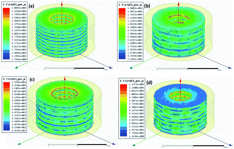 | ||
| Fig. 6 Electric field dissipation characteristic and dispersion magnitudes for EM waves in the absorbers. (a) GMT10, (b) GMT30, (c) GMT50, and (d) GT composite samples. | ||
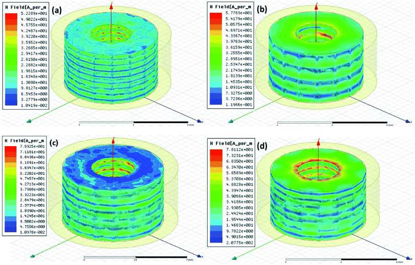 | ||
| Fig. 7 Magnetic field dissipation characteristics and dispersion magnitudes for EM waves in the absorbers. (a) GMT10, (b) GMT30, (c) GMT50, and (d) GT composite samples. | ||
The color in each figure corresponds to the standard scale on the left, as shown in Fig. 6 and 7. This is the amplitude distribution of the EM induction intensity due to the adjustment of the composites in the absorbers, of which the composite properties changed for the absorber samples. In general, the absorber color near the center is orange-yellow. The magnitudes of the E field from magnetic induction are about 1.7588 × 100 to 2.0064 × 10⁴, 3.2942 × 10⁻¹ to 1.5009 × 10⁴, 6.8376 × 10⁻¹ to 1.3258 × 10⁴, and 1.4399 × 100 to 1.2373 × 10⁴ V m−1, respectively, as shown in Fig. 6 from (a) to (d). These magnitudes are achieved from an automatically defined scale of simulation, indicating the existing values in the nephograms. However, E field magnitude distribution cannot distinguish the obvious differences among the GMT10, GMT30, GMT50, and GT composite samples. Meanwhile, the minimal standard scale for GMT30 is less than that for other composite absorbers, implying a small E field in GMT30. The magnitude of the scales for these samples is equivalent. Periodic variation of the scaled color in absorbers is related to the periodic propagation of the EM wave, agreeing with the dispersion of EM waves for simulations in metamaterials.30
Correspondingly, from (a) to (d) in Fig. 7, the respective magnitudes of the H field from electric induction are 1.0419 × 10⁻² to 5.2289 × 101, 1.1966 × 10⁻¹ to 5.7783 × 101, 1.0978 × 10⁻² to 7.5925 × 101, and 2.0775 × 10⁻² to 7.8112 × 101 A m−1, respectively. The absorber color away from the sample center is blue or green in the periodic distribution, resulting from periodic microwave propagation. Additionally, the minimal standard scales are different; GMT30 has the strongest minimal value; GMT10 and GMT50 have weak minimal value, among these samples. The magnitudes of the large values of these composites are similar. Composite property effects on the absorbers are not distinguished from the E field or the H field, but only indicate some transition in the field response near the GMT30 and GMT50 absorbers. Compared with the magnitude of electric fields, the magnetic part has a small magnitude, while the electric field has a large magnitude. The relation between the electric and magnetic fields agrees with the tangent loss distinguishment in the following section. The characteristics of the EM fields in the composites demonstrate that they are electromagnetic compatibility (EMC) absorbers.
A different magnitude of EM induction was obtained by changing the parameters of the absorbers in the simulation. Variance of EM parameters results from filler components and semiconductor modulation in absorber composites. Dispersion of fields indicates complex reflection effects of EM fields in the absorber. However, EM fields, especially the components of E or H, can only provide partial information regarding reflection loss. Comprehensive energy related to EM fields is a key index for EM decay. In terms of EM theory, the Poynting vector characterizes the energy propagation. Dispersion of the Poynting vector can be achieved, as provided in Fig. S1 of the ESI.† The energy flux densities of GM, GMT10, GMT30, GMT 50 and GT respectively cover the ranges of 1.3487 × 100 to 1.1454 × 10³, 2.4322 × 10⁻¹ to 1.7555 × 10³, 3.9571 × 10⁻¹ to 7.4762 × 10², 7.6080 × 10⁻¹ to 1.3651 × 10⁴, and 4.1940 × 10⁻¹ to 1.7135 × 10³ W m−2. The unit W m−2 of the Poynting vector is exactly the unit of the energy flux density. Among these estimated results, the intermediate value of energy flux of GMT30 is 3.7401 × 10² W m−2. GMT30 possesses the lowest flux density in general, implying high energy absorption in composites, which is consistent with the experimental results of large reflection loss. However, for the case of titania semiconductor as the main component, there is relatively low flux density in the GT composite. The results for the GT composite may be due to the peak frequency shift near 12 GHz. This frequency is different from the other cases, with the max peak frequency near 14–15 GHz, as listed in Table 1. These phenomena are attributed to the crossing band effect. The Poynting vector is no more than the magnitude of 103 W m−2 for all these composites. Comparing the incident wave energy density of about 104 magnitude for 1 W in several tens of square millimeters, a large part of the density flux in the absorber dissipates. The large decay of EM waves in the absorber is also consistent with the characteristic of exponential rule.31 In fact, both the electric field and magnetic field simulations present homogeneity of the fields for the calculation rules of setting. The homogeneity of the fields from the simulation match the results of the real samples, implying that the measured parameters as set in the simulation are reliable.
3.3 Modulation effects from loss tangent and reflection loss
Tangent loss is a way to evaluate the EM wave dissipation in an absorber. The tangent loss includes the total tangent loss, electric tangent loss, and magnetic tangent loss, as shown in Fig. 8. The total tangent loss reflects the total effect of absorbing dissipation, similarly to reflection loss. The electric tangent loss and magnetic loss demonstrate the electric loss and magnetic loss, respectively. The absolute value of the magnetic loss is generally less than that of the electric loss, implying that electric loss is the predominant type. However, for the semiconductor-added absorber GMT30, the inverse occurs, in which the absolute value of the magnetic loss is larger than that of the dielectric loss. This inverse loss type indicates that an extreme situation is taking place, matching the inflection point in the mathematical rule.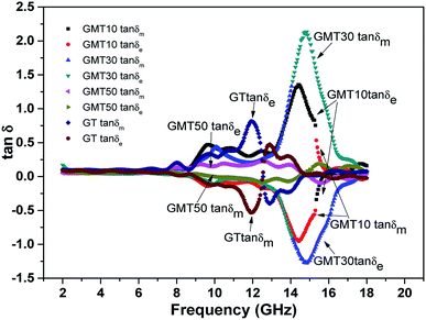 | ||
| Fig. 8 Variation of the dielectric and magnetic loss tangents with frequency for the titania-doped composites. | ||
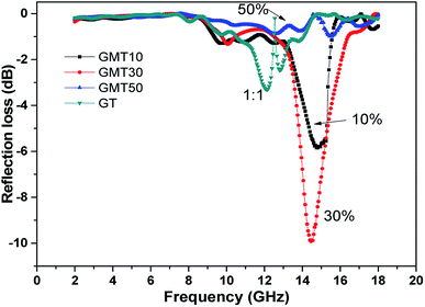
The absorption performance of the samples with the addition of titania is presented in Fig. 9. The peak values of reflection loss for the GT absorber in the ranges of 9.15–12.5 GHz and 12.55–14.35 GHz are 3.31 and 2.47 dB, respectively. These values are generally lower than those for the cases of composites containing GNS and EMO.3 However, addition of titania to the GNS-EMO composites enhances the reflection loss; for example, the reflection loss of the GMT30 sample is enhanced to 9.91 dB. With low semiconductor contents as additives, the enhanced effects assist the composites to almost reach the desirable properties of microwave absorbers.32,33 The GMT30 sample shows an obvious improvement compared with 4.78 dB for the composite-filled equal mixtures of GNS-EMO. The enhanced values are also larger compared with the composites with only GNS and EMO components, with 4.25 dB for the electric loss and 7.19 dB for the magnetic loss. The ratios of GNS to EMO are 1![[thin space (1/6-em)]](https://www.rsc.org/images/entities/char_2009.gif) :
:![[thin space (1/6-em)]](https://www.rsc.org/images/entities/char_2009.gif) 5 to 5
5 to 5![[thin space (1/6-em)]](https://www.rsc.org/images/entities/char_2009.gif) :
:![[thin space (1/6-em)]](https://www.rsc.org/images/entities/char_2009.gif) 1 when not considering the matching volume with resin.3 The reflection loss, almost reaching around 10 dB, can be directly applicable simply due to the modulation of the composites. This magnitude is consistent with a similar filled paraffin absorber with the same thickness.33
1 when not considering the matching volume with resin.3 The reflection loss, almost reaching around 10 dB, can be directly applicable simply due to the modulation of the composites. This magnitude is consistent with a similar filled paraffin absorber with the same thickness.33
However, the reflection loss does not monotonically increase as the titania content increases in the composites. GMT50 has a small reflection loss of no more than 1 dB. The reflection loss of GMT50 is smaller than that of GMT30. The large reflection loss of 3.31 dB for the GT composite is also less than 9.91 dB for GMT30. Moreover, the GT composite is an extreme situation among graphene-based resin absorbers. The GT composite has a high content of titania, reaching an equal quantity to that of GNS. Furthermore, the composites with the full ratio of titania have low response parameters due to the real and imaginary parts of the composite permittivity of titania. Especially, the imaginary parts of titania composites are near zero.26 The characteristics of titania composites imply almost transparent performance to radiation for titania composites. Therefore, the addition of a semiconductor has a modulation function to improve electric and magnetic-integrated absorbing materials. Titania semiconductor should not be taken as a main component in a composite absorber. Table 1 provides the peak values and the corresponding bands in the range of 2–18 GHz. The resonance bands mainly belong to the X and Ku bands. When the composites contain low titania contents, the peak frequencies for the strong reflection loss show slight blue shifts. The enhancement is obvious in contrast to the absorbers with no titania, unsuitable ratios and high contents of titania. The optimal range is near 30 percent, which is consistent with the ratio regularity of TiO2–Ti3C2Tx graphene film.21 These titania content characteristics are in accord with literature reports that a medium ratio of TiO2 achieves excellent absorption properties.33 The absorption properties do not often monotonously increase as the titania contents increase or decrease. The nonmonotonicity of reflection loss agrees with the magnitude of the simulated EM fields in absorbers. The enhancement is even larger than that resulting from the directly increased magnetic component of the same ratio in the literature.2
3.4. Occupying dissipation theory for semiconductor modulation with uniformity
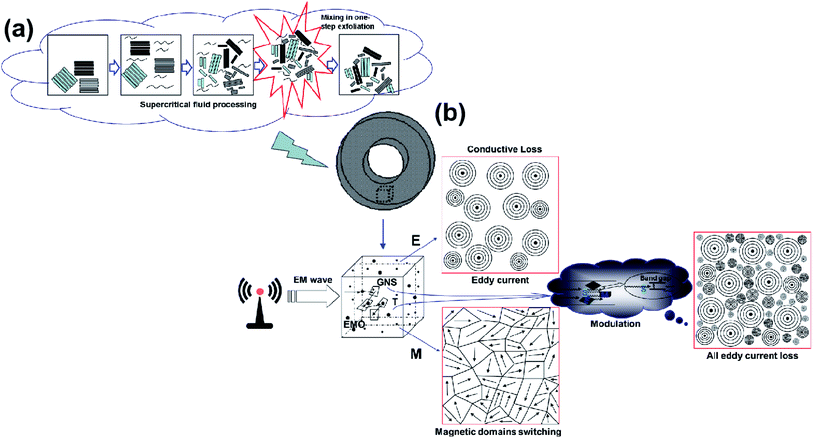
Exfoliation takes place during supercritical processing, as reported in ref. 11 and 13. The situation of multi-component exfoliation is shown in inset (a) of Fig. 10. During the exfoliation processing, random mixing of multi-components occurs naturally. The reasons for the mixing of the exfoliated products include two aspects. The first aspect is fluid dynamics. As the fluid reaches the supercritical state, fluid molecules have high energy during fierce motion. The amounts of molecules with high energy impact the dispersed matter or exfoliated products. The dispersed tiny materials randomly move in any possible direction. Thus, their relative positions are random. Diffusive mixing is enhanced. Convective mixing takes place. These mixing forms agree with the mixing mechanisms.8 The random relative positions of the different component materials occur after precipitation due to supercritical state termination. The properties of the obtained mixtures result from the uniformity of the constituent material components. The other aspect is the random rearrangement of exfoliated products, resulting from scattering during exfoliation. This course covers the shear mixing. All these mixing factors give rise to fine mixing of multi-components. Mixing results are desired for ideal media to achieve homogeneity in scientific research.5 Mixing dispersion not only results in homogeneity for ideal media, but also provides superior topology for titania modulation dissipation.From the general electric resistivity dissipation relation, the eddy current i = Φ/R. R is determined by the property of conductivity. Φ is the induced electromotive force from the EM wave induction. For conductors, Φ already determines the eddy current. Current dissipation is one of the reasons for the maximum absorption of conductive-type absorbers. From theoretical consideration, if magnetic loss results mainly from eddy current loss, the value of C0 = μ′′(μ′)−2f−1 should be constant when the frequency is varied.34,35 It is obvious that the C0 value is steady in the 2–18 GHz frequency range, although there are tiny fluctuations on an extremely small scale (Fig. S2† and its inset). This small scale is far smaller than the tolerance error. Therefore, eddy current loss is one of the main electromagnetic loss types. Because the incident EM wave acts on magnetic components, magnetic domains of magnetic materials in composites shift their magnetization direction along with EM induction. Conversely, shifting of the magnetizing direction to regular frequency gives rise to electric induction, resulting in electric dissipation. Meanwhile, partial heat consumption results from repetitive shifting of the magnetic domains. All these courses consist of magnetic dissipation. These dissipation courses are demonstrated in Fig. 10(b). The response of the magnetic domains limits infinite absorption. Furthermore, magnetic domain shift consumption is weak dissipation. Consequently, any electric loss or magnetic loss is finally dissipated into thermal energy.36 The heat is produced from resistance of the eddy current by i2R. This is the reason for the high heat that is sometimes felt in absorbing measurements. Based on the mechanisms in the literature, in addition to multi reflection and scattering,37 eddy currents and magnetic domains are emphasized.38 Moreover, semiconductor modulation plays a crucial role. The addition of a semiconductor is expected to adjust the microwave absorption in composites. In energy band theory, for the excitation hv ≥ hv0 = Eg, where h is the Planck constant, a frequency shift of v − v = Δv is produced. Compared with the absorber sample with no semiconductor addition, blue shift of reflection loss takes place for the absorber with added semiconductor due to the frequency shift resulting from the semiconductor.
Semiconductor addition is a crucial factor for the properties of a composite. The modulation mechanism of a semiconductor from its physical nature elucidates the absorbing effect. Occupying theory is proposed to describe the dissipation. Area occupation is for a scenario from the cross-section of composites. Treating every eddy current as a dissipation piece, many pieces take up the section area. All the eddy currents, including the eddy currents induced by the conductor and semiconductor, take up all the area one by one. Then, the modulation mechanism results agree with the literature.38,39 Excessive pieces taking up space in a unit area give rise to current overlap. Overlap of induced current is ineffective because the pieces offset each other with regard to the determined resistivity and electromotive force. Only taking up empty space is effective for enhancement of dissipation. Fortunately, the uniform mixing in SCF results in a random dispersion of fillers. Especially, the scattered semiconductor components in the fillers reduce the possibility of overlap before reaching the optimal percentage. Fully efficient occupation of blank areas with eddy currents determines the greatest enhancement of dissipation, corresponding to the maximum reflection loss. The components and physical properties of a semiconductor determine the inductive eddy current within a range of sizes, which are normally smaller than the eddy currents directly produced in conductors. The conductor components determine the main eddy currents resulting from the conductors. Semiconductor eddy currents fill the blanks among the conductive eddy currents. When the unit area is full, the dissipation of microwave induction electromotive force reaches a critical dissipation. The much greater amount of eddy current produced contributes little to a full unit. Moreover, no eddy current is produced in the limited space any more. Overlap of eddy currents gives rise to unobvious enhancement of current dissipation; however, some depression occurs from the offset effect. Thus, the absorbing effect is reduced when the semiconductor components exceed a certain percentage. Therefore, the increased absorbing effect from GMT10 to GMT30 and the decreased effect from GMT30 to GMT50 for the titania-modulated samples is acceptable. In fact, the semiconductor modulation improves the impedance matching for dissipation enhancement, agreeing with the mechanism in ref. 38. The tri-dimensional occupation situation has similar rules to area occupation. Eddy current often behaves in a plane. Hence, area occupation is optional for theoretical explanation.
The dissipation enhancement effect agrees with several cases in the literature, such as the cases of TiO2 introduction into ZnFe2O4 and graphene composites in ref. 28 and 32. This indicates that the semiconductor titania gives rise to enhanced absorption, as evaluated from the absorption of samples of the same thickness reported in Table S1 of the ESI.† For the 4 mm-thick uniform samples, the increment of reflection loss has a similar magnitude to that between magnetic graphene and magnetic graphene@porous TiO2 composites in the low frequency end28 and to that between ZnFe2O4@graphene and ZnFe2O4@graphene@TiO2 composites in the high frequency end.32 However, TiO2 in the literature arises from reaction products of reagents. The scheme in this work involves direct addition of titania to reveal its essential attributes; thus, this addition is more reasonable to directly display the nature of titania.
3.5. Simulation consistency of semiconductor modulation scheme
The relation between the semiconductor content and peak reflection loss of the composites is exhibited in Fig. 11, including the case without semiconductor. The initial point of zero titania content is the case of GM composites in previous work.3 The end point for GT composites is the case for only titania in graphene-based composites. There is a peak range among these samples. The trend curve of these peak data matches the Gaussian fitting. The trend rule for these data implies that there is an optimal range for semiconductor addition as a filler component for absorbers. Optimal semiconductor addition leads to high reflection loss. Low ratio modulation results in low occupancy. High ratio modulation gives rise to overlapped occupancy of space. Hence, a suitable ratio will obtain an optimal occupying effect. Occupying theory gives reasons on semiconductor improvement, which can explain the existing peaks for small quantity addition. The blue shift is also clarified by the frequency shift Δv. The center values from the Poynting distribution are exhibited in Fig. 11, as achieved from standard color scale bars in Fig. S1 of the ESI.† The intermediate value can be taken as a typical value to differentiate the general situation of EM energy distribution among these absorbers. Compared with the reflection loss curve, the flux density has a converse trend, as shown by the dashed line in Fig. 11. For the high reflection loss case, the flux density is relatively low. The low flux density indicates a high absorbing effect. There is a trough among these samples from the trend line of flux density. These results are in accordance with the reflection loss trend from a contrasting trend.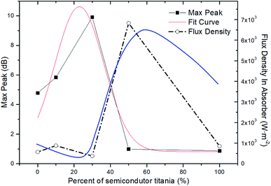 | ||
| Fig. 11 Relations among the titania semiconductor content of the composites, peak reflection loss of the composites, and flux density in the absorbers. | ||
Unless the media are uniform or at least the fully mixed fillers are uniformly dispersed, the fields in a real absorber will be regular. The uniform dispersion of fully mixed fillers with micro-nano sizes will only give rise to local distortion of fields. The whole fields in the sample absorbers are homogeneous on the macro scale. In this case, the simulation results match the results from the tests. Therefore, fully mixing fillers in a uniform dispersion state enables the collection of reasonable parameters in the simulation. Conversely, the simulation consistency reflects that the fully mixed fillers result in homogeneity of the absorbers. The simulation trend of the series of absorbers is consistent with the trend of the test results in Fig. 11, confirming the effectiveness of the contribution of uniformity by the SCF method. Overall, the effects of semiconductor modulation are confirmed from the field simulation and the reflection loss.
4. Conclusions
The EM absorbing scheme of semiconductor modulation of surface composites is confirmed. Precursors were exfoliated by the fast exfoliation of SCF. The harsh reaction conditions in SCF result in adequate premixing of the filler components during exfoliation. EM-absorbing composite samples were achieved using a casting solidification moulding method. Microscopic characterization demonstrated that the fillers are dispersed uniformly in the resin matrix. The formed composites approach ideal medium states for absorbers. Simulations of EM waves propagating in the absorbers were used to estimate the dissipation in the composites according to the dielectric and magnetic property parameters in the resonance region. GMT30 composite has a low energy flux with an intermediate value of 3.7401 × 10² W m−2 for the propagating EM wave. GMT30 composite with 30 percent titania added as filler showed the largest reflection loss, reaching 9.91 dB. The simulation estimations were consistent with the reflection loss results. The peak frequency was located at 14.45 GHz in the peak range of 7–17 GHz.The reflection loss does not increase monotonically as the semiconductor content increases. The optimal proportion of absorbing semiconductor modulation is between 10 percent and 50 percent. Compared with the main filler components of exfoliated GNS and EMO, small amounts of semiconductor titania component result in enhanced loss. These results reveal that the proposed scientific scheme is effective for the development of absorbers. Simulations of the EM wave energy flux density agreed with the trend of reflection loss in a series of samples.
Conflicts of interest
There are no conflicts to declare.Acknowledgements
The authors acknowledge the support from Talent Start-up Project of Nanchang Hangkong University (EA201906235), National Natural Science Foundation of China (No. 51965041), and meanwhile thank the Instrumental Analysis Center of SJTU for some of the tests.References
- Z. Chen, C. Xu, C. Ma, W. Ren and H.-M. Cheng, Adv. Mater., 2013, 25, 1296–1300 Search PubMed.
- B.-J. Kim, K.-M. Bae, Y. S. Lee, K.-H. An and S.-J. Park, Surf. Coat. Technol., 2014, 242, 125–131 Search PubMed.
- L. Yi, G. Hu and H. Li, Composites, Part A, 2015, 76, 233–243 Search PubMed.
- C. Mingdong, Y. Huangzhong, J. Xiaohua and L. Yigang, Appl. Surf. Sci., 2018, 434, 1321–1326 Search PubMed.
- S. Giordano, J. Electrost., 2003, 58, 59–76 Search PubMed.
- J. Sax and J. Ottino, Polym. Eng. Sci., 1983, 23, 165–176 Search PubMed.
- F. Cansell and C. Aymonier, J. Supercrit. Fluids, 2009, 47, 508–516 Search PubMed.
- J. Gyenis, Chem. Eng. Process., 1999, 38, 665–674 Search PubMed.
- P. M. C. Lacey, J. Appl. Chem., 1954, 4, 257–268 Search PubMed.
- N.-W. Pu, C.-A. Wang, Y. Sung, Y.-M. Liu and M.-D. Ger, Mater. Lett., 2009, 63, 1987–1989 Search PubMed.
- D. Rangappa, K. Sone, M. Wang, U. K. Gautam, D. Golberg, H. Itoh, M. Ichihara and I. Honma, Chem.–Eur. J., 2010, 16, 6488–6494 Search PubMed.
- L. Yi and G. Hu, RSC Adv., 2013, 3, 23461–23469 Search PubMed.
- G. Hu, L. Yi and C. Liu, J. Supercrit. Fluids, 2012, 72, 59–67 Search PubMed.
- L. Yi, G. Hu and H. Huang, Powder Technol., 2014, 259, 109–116 Search PubMed.
- L. Yi, G. Hu, J. Hou and L. Li, J. Supercrit. Fluids, 2014, 95, 24–34 Search PubMed.
- Y. Omomo, T. Sasaki, L. Wang and M. Watanabe, J. Am. Chem. Soc., 2003, 125, 3568–3575 Search PubMed.
- M. Naebe, J. Wang, A. Amini, H. Khayyam, N. Hameed, L. H. Li, Y. Chen and B. Fox, Sci. Rep., 2014, 4, 4375 Search PubMed.
- T. Sasaki, M. Watanabe, Y. Michiue, Y. Komatsu, F. Izumi and S. Takenouchi, Chem. Mater., 1995, 7, 1001–1007 Search PubMed.
- D. C. L. Vasconcelos, V. C. Costa, E. H. M. Nunes, A. C. S. Sabioni and W. L. Vasconcelos, Mater. Sci. Appl., 2011, 02, 1375–1382 Search PubMed.
- M. Hema, A. Y. Arasi, P. Tamilselvi and R. Anbarasan, Chem. Sci. Trans., 2013, 2, 239–245 Search PubMed.
- C. Xiang, R. Guo, S. Lin, S. Jiang, J. Lan, C. Wang, C. Cui, H. Xiao and Y. Zhang, Chem. Eng. J., 2019, 360, 1158–1166 Search PubMed.
- D. T. On, Langmuir, 1999, 15, 8561–8564 Search PubMed.
- P. A. Connor, K. D. Dobson and A. J. McQuillan, Langmuir, 1999, 15, 2402–2408 Search PubMed.
- M. G. González, J. C. Cabanelas and J. Baselga, Infrared Spectrosc.: Mater. Sci., Eng. Technol., 2011, 261–284 Search PubMed.
- K. Chike, M. Myrick, R. Lyon and S. Angel, Appl. Spectrosc., 1993, 47, 1631–1635 Search PubMed.
- H.-M. Xiao, X.-M. Liu and S.-Y. Fu, Compos. Sci. Technol., 2006, 66, 2003–2008 Search PubMed.
- Y. Cheng, J. Z. Y. Seow, H. Zhao, Z. J. Xu and G. Ji, Nano-Micro Lett., 2020, 12, 125 Search PubMed.
- P. Liu, Y. Huang, J. Yan and Y. Zhao, J. Mater. Chem. C, 2016, 4, 6362–6370 Search PubMed.
- ANSYS Reference Manual, Release 5.7, 1999.
- X. Q. Lin, T. J. Cui, J. Y. Chin, X. M. Yang, Q. Cheng and R. Liu, Appl. Phys. Lett., 2008, 92, 131904 Search PubMed.
- L.-L. Zhang and Y. Chen, in TBIS Proc., 2010, pp. 1022–1027 Search PubMed.
- Y. Wang, H. Zhu, Y. Chen, X. Wu, W. Zhang, C. Luo and J. Li, Mater. Chem. Phys., 2017, 202, 184–189 Search PubMed.
- G. Mu, N. Chen, X. Pan, K. Yang and M. Gu, Appl. Phys. Lett., 2007, 91, 043110 Search PubMed.
- M. Wu, Y. D. Zhang, S. Hui, T. D. Xiao, S. Ge, W. A. Hines, J. I. Budnick and G. W. Taylor, Appl. Phys. Lett., 2002, 80, 4404–4406 Search PubMed.
- X. Liang, Z. Man, B. Quan, J. Zheng, W. Gu, Z. Zhang and G. Ji, Nano-Micro Lett., 2020, 12, 102 Search PubMed.
- Y. Lin, J. Dai, H. Yang, L. Wang and F. Wang, Chem. Eng. J., 2018, 334, 1740–1748 Search PubMed.
- X. Yuan, R. Wang, W. Huang, Y. Liu, L. Zhang, L. Kong and S. Guo, Chem. Eng. J., 2019, 378, 122203 Search PubMed.
- X. Xu, G. Wang, G. Wan, S. Shi, C. Hao, Y. Tang and G. Wang, Chem. Eng. J., 2020, 382, 122980 Search PubMed.
- H. Zhang, G. Zhang, Q. Gao, M. Tang, Z. Ma, J. Qin, M. Wang and J.-K. Kim, Chem. Eng. J., 2020, 379, 122304 Search PubMed.
Footnote |
| † Electronic supplementary information (ESI) available. See DOI: 10.1039/d0ra08557j |
| This journal is © The Royal Society of Chemistry 2020 |

