
Branched polymer-incorporated multi-layered heterostructured photoanode: precisely tuning directional charge transfer toward solar water oxidation†
Zhi-Quan
Wei
,
Xiao-Cheng
Dai
,
Shuo
Hou
,
Yu-Bing
Li
,
Ming-Hui
Huang
,
Tao
Li
,
Shuai
Xu
and
Fang-Xing
Xiao
 *
*
College of Materials Science and Engineering, Fuzhou University, New Campus, Minhou, Fujian Province 350108, China. E-mail: fxxiao@fzu.edu.cn
First published on 27th November 2019
Abstract
Unidirectional and smooth charge transfer to the reactive sites plays an imperative role in boosting the solar-to-hydrogen conversion efficiency of photoelectrochemical (PEC) cells but suffers from sluggish charge transfer kinetics. Herein, as a proof-of-concept demonstration, high-speed spatially separated electron and hole transfer channels were simultaneously constructed in an integrated multilayered heterostructured photoanode via an efficient electrostatic layer-by-layer (LbL) assembly strategy, wherein a tailor-made positively charged polymer of branched polyethylenimine (BPEI) and negatively charged MoS2 quantum dot (QD) building blocks were intimately and alternately integrated on the hierarchically ordered TiO2 nanotube array (TNTA) framework in a unique “face-to-face” stacking fashion. The periodically alternately stacked ultra-thin BPEI layer in the ternary multilayered photoanode serves as a directional hole transport channel and the MoS2 QD layer functions as a cascade electron transfer channel, which synergistically contribute to the considerably enhanced separation and prolonged lifetime of charge carriers, endowing the multilayered TNTAs/(BPEI–MoS2 QDs)n photoanodes with markedly enhanced PEC water dissociation performances with respect to the single and binary counterparts under simulated solar light irradiation. Moreover, the essential role of the assembly unit was clarified. Our work would afford a new frontier to intelligently mediate the photoinduced charge flow by rationally constructing the unidirectional charge transport channels in semiconductor-based photoelectrodes for solar energy conversion.
1. Introduction
Solar energy collection, conversion and storage can be integrated in a single photoelectrochemical (PEC) cell in the simplest chemical bond (viz., H–H).1 Semiconductor-based PEC water splitting has been attracting enormous interest since the discovery of the Honda–Fujishima effect in the early 1970s.2,3 Various nanostructured metal oxides have thus been explored for PEC water splitting, among which one-dimensional (1D) semiconductors stand out among fruitful semiconductors due to their unique structural advantages compared with nanoparticulate and bulk counterparts, such as fast and long-distance electron transport, larger specific surface area, and enhanced light absorption and scattering capabilities.4–6Particularly, 1D TiO2-based semiconductors growing from conducting substrates (e.g., Ti foil or FTO) have been extensively exploited for PEC water splitting owing to their fascinating merits such as non-toxicity, excellent photostability, and high-efficiency charge transfer along the vertical direction of the 1D framework.7–9 Nevertheless, the high recombination rate of charge carriers and poor light absorption in the visible and near-infrared regions of the solar spectrum hinder the development of 1D TiO2, which leads to low quantum efficiency of PEC reactions.10,11 As such, multifarious strategies have been developed, e.g., metal deposition (Pd, Au, Ag, Pt),12–15 metal or non-metal (C, N, B, S) elemental doping,16–18 photosensitization with narrow-band-gap semiconductor quantum dots (e.g., CdS, CdSe, CdTe, PbS),19–21 construction of p–n heterojunctions (e.g., Cu2O, NiO)22,23 and hybridization with carbon materials (e.g., graphene, carbon nanotubes),24–26 to reduce the bandgap or extend the light-responsive region to the visible or near-infrared domain.27,28 Of particular note is the decoration of TiO2 with metal nanocrystals (NCs) in terms of the lower Fermi level of metal NCs for triggering the Schottky-junction-driven charge flow. Although metal NC deposition can benefit the interfacial charge transfer, rational construction of charge transfer channels with a controllable interface in an integrated PEC cell is in the infant stage. Besides, the prohibitive cost and scarcity of metal NCs restrict their wide-spread applications. Therefore, it is highly desirable to seek suitable alternatives to metal NCs to stimulate the interfacial charge transfer kinetics for considerably enhanced charge separation. Notably, earth-abundant transition metal chalcogenides (TMCs: e.g., MoS2, MoSe2, WS2etc.) enable boosted electron transfer in photocatalytic and PEC water splitting.29 Considering that solar-to-hydrogen conversion efficiency is heavily dependent on the interface between the TMCs and semiconductors, elaborate interface design and engineering would play a synergistic role, which calls for a novel material-manipulating strategy.
The layer-by-layer (LbL) assembly technique, as a promising bottom-up technique, demonstrates many advantages with respect to the conventional approaches in terms of simplicity, applicability and versatility, which furnishes tunable control over the microstructure, thickness, and composition of the assemblies.4,30,31 By rationally tuning the category of materials and deposition sequence, diverse nanostructured building blocks with distinct structures and compositions can be harmoniously integrated within the multilayered films, resulting in hybrid nanostructures with collective and improved functional properties.32 Inspired by this, if oppositely charged TMCs and polyelectrolyte (PE) were selected as the building blocks and alternately deposited on the semiconductor in a “face-to-face” stacking fashion via the LbL assembly, integration mode and interface engineering between TMCs and semiconductor can be finely modulated with the assistance of PE, resulting in (PE/TMDs)n/semiconductor multilayered heterostructures. In this way, spatially separated unidirectional electron–hole charge transfer channels in the (PE/TMDs)n/semiconductor multilayered heterostructures can be exquisitely designed in advance by finely tuning the assembly sequence and the number of assembly bilayers. On the other hand, it should be stressed that PEs are generally utilized as the “molecular glue” in the LbL assembly to facilitate electrostatic attraction with the oppositely charged counterparts and removal of PEs is normally necessary for achieving intimate interfacial integration among the building blocks.11,33 Thus far, utilizing PE as an interfacial charge transfer mediator has not yet been reported.
With these motivations, herein, an efficient LbL assembly strategy was developed to construct multilayered heterostructured photoanodes, wherein the positively charged PE of branched polyethylenimine (BPEI) and negatively charged MoS2 quantum dot (QD) building blocks were alternately deposited on TiO2 nanotube arrays (TNTAs) based on the electrostatic interaction. The intrinsically positively charged surface and the strong reducibility of BPEI make the ultra-thin BPEI layer a high-efficiency hole-transporting mediator and the MoS2 QD layer the electron-withdrawing medium, which concurrently constitute two spatially separated charge transfer channels in the multilayered photoelectrodes. The unique multilayered nanoarchitecture and alternate integration fashion at the nanoscale level endow multilayered TNTAs/(BPEI–MoS2 QDs)n ternary heterostructures with superior PEC water splitting performances under simulated solar light irradiation. This is predominantly ascribed to the fact that alternate integration of ultra-thin BPEI layer and MoS2 QDs endowed by the LbL assembly is beneficial for precisely regulating the unidirectional migration of photoinduced holes and electrons, strategically enhancing the charge separation.
2. Experimental section
2.1. Preparation of the TNTA substrate and MoS2 quantum dots (QDs)
A two-step anodizing method was employed to prepare TNTAs by referring to the previous work by Xiao et al.16 Meanwhile, preparation of MoS2 QDs was also adopted from a published report.34 For more experimental details see the Experimental section in the ESI.†2.2. Preparation of TNTAs/(BPEI/MoS2 QDs)n heterostructures
The TNTA substrate was first dipped into the positively charged BPEI aqueous solution (0.5 mg mL−1, 0.5 M NaCl, pH = 10) for 5 min and then washed with DI H2O for 1 min. Subsequently, BPEI-modified TNTAs were dipped into the negatively charged MoS2 QD aqueous solution (150 mg L−1, pH = 4.57) for 5 min, after which the sample was washed with DI H2O for 1 min and dried with a stream of N2. The above fabrication process was defined as one bi-layer, i.e., [TNTAs/(BPEI/MoS2 QDs)1]. According to the above synthesis procedure, multilayered TNTAs/(BPEI–MoS2 QDs)n heterostructures were fabricated via an analogous LbL assembly route.2.3. Characterization
Zeta potential (ξ) measurements were performed by dynamic light scattering analysis (Zeta sizer Nano ZS-90) by repeating five measurements at room temperature (298 K) and pH values of the samples were carefully adjusted with diluted 0.1 M HCl or NaOH aqueous solution. Crystal structures were determined by X-ray diffraction (XRD, X'Pert Pro MPD, Philips, Holland) using Cu Kα as the radiation source at 40 kV and 40 mA. Morphologies of the samples were probed by field emission scanning electron microscopy (FESEM, Supra55, Carl Zeiss, Germany) equipped with an energy-dispersive spectroscopy (EDS) setup. Transmission electron microscopy (TEM) and high-resolution TEM (HRTEM) images were collected on a JEOL-2010 with an accelerating voltage of 200 kV. Fourier transform infrared (FTIR) spectra were recorded on a TJ270-30A infrared spectrophotometer (Tianjin, China). X-ray photoelectron spectroscopy (XPS) spectra were recorded on a photoelectron spectrometer (ESCALAB 250, Thermo Fisher Scientific, USA), where the binding energy (B.E.) of the elements was calibrated using the B.E. of C 1s (284.60 eV). UV-vis diffuse reflectance spectra (DRS) (Cary50 UV-vis spectrophotometer, Varian, USA) were obtained using BaSO4 as the reflectance background ranging from 250 to 800 nm. Raman measurements were carried out by Raman spectroscopy (Dxr-2xi, Thermo Fisher Scientific, USA) with an extended scan range of 0–3000 cm−1. Photoluminescence (PL) spectra were collected on a Varian Cary Eclipse spectrometer.2.4. PEC water splitting measurements
PEC water splitting measurements were performed using a conventional three-electrode configuration on an electrochemical workstation (CHI660E, CHI Shanghai, Inc.). TNTAs, TNTAs/(BPEI/MoS2 QDs)n [T(BM)n] (n = 1, 2, 4, 6, 8), TNTAs/(BPEI)2 [TB2], TNTAs/(MoS2 QDs)2 [TM2], and Ti(BM)2 (1 cm × 1 cm) were directly employed as the working electrodes, and Pt foil and Ag/AgCl electrode as the counter and reference electrodes, respectively. The electrolyte was composed of 0.5 M Na2SO4 (pH = 6.69) aqueous solution. PEC water splitting performances were evaluated under simulated sunlight irradiation from a 300 W Xe lamp (FX300, Beijing Perfect Light Co. Ltd, China) equipped with an AM 1.5G filter or visible light (λ > 420 nm). Potentials of the electrodes were calibrated against the reversible hydrogen electrode (RHE) based on the formula given below: | (1) |
3. Results and discussion
The overall fabrication procedures for the LbL assembly of TNTAs/(BPEI–MoS2 QDs)n heterostructures, i.e., T(BM)n (n = 1, 2, 4, 6, 8) are illustrated in Scheme 1. In the first step, the hierarchically ordered TNTA substrate was prepared by a two-step electrochemical anodization approach. It has been well-established that TNTAs consisting of periodically arranged top-porous layers and vertically aligned bottom tubular arrays afford much less structural defects as compared with TNTAs prepared via the conventional one-step anodization approach,16 making them a suitable 1D semiconductor framework for the LbL assembly buildup. Dipping TNTAs into BPEI aqueous solution (pH = 10) endows the TNTA substrate with a negatively charged surface in view of the isoelectric point of TiO2 (4.2–6.8).35 In this regard, the positively charged ultra-thin BPEI layer can be electrostatically self-assembled on the negatively charged TNTAs, which affords a positively charged surface of TNTAs. The spontaneous adsorption of BPEI on the TNTA surface arises from its unique structure that is characterized by the presence of a large amount of amine groups (Table S4†), which endow BPEI with high affinity to the hydrophilic TNTA surface. Based on this, positively charged BPEI can be uniformly assembled on the TNTA substrate for the following spontaneous electrostatic assembly buildup with the tailor-made negatively charged MoS2 QDs (Fig. S1†), resulting in the T(BM)1 heterostructure.32,36 Then, in the same way, the thus-obtained T(BM)1 heterostructure was alternately re-treated with BPEI and assembled with MoS2 QDs based on the pronounced electrostatic interaction, by which the deposition amount of BPEI and MoS2 QDs on the TNTA substrate was finely tuned by the assembly cycle, ultimately resulting in well-defined T(BM)n (n = 1, 2, 4, 6, 8) multilayered heterostructures.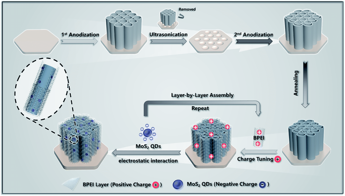 | ||
| Scheme 1 Schematic illustration for the electrostatic LbL assembly of TNTAs/(BPEI–MoS2 QDs)n ternary multilayered heterostructures. | ||
3.1. Characterization of composite photoanodes
Our work begins with the characterization of the photoanodes. The crystal structure of the samples was probed by X-ray diffraction (XRD) spectra. Fig. 1a shows the XRD patterns of blank Ti foil, TNTAs, Ti(BM)2, and T(BM)2 heterostructures, wherein the diffraction peaks at 2θ values of 25.5°, 38.1°, 48.2°, 54.4°, and 55.3° are undisputedly indexed to the (101), (004), (200), (105), and (211) crystal planes of anatase TiO2 (JCPDS no. 21-1272) and the peaks at 38.6°, 40.3°, 53.1°, 63.0°, 70.8°, and 76.3° match well with the metallic Ti phase (JCPDS no. 44-1294) from Ti foil. It is worth noting that these characteristic diffraction peaks corresponding to anatase TiO2 are concurrently observed in the XRD patterns of T(BM)2 and TNTAs, suggesting that the crystal structure of the TNTA framework was retained after the attachment of BPEI and MoS2 QDs. Alternatively, XRD patterns of T(BM)n (n = 1, 4, 6, 8) were also probed and the results are displayed in Fig. S2,† from which it is clearly seen that all these samples exhibit almost the same characteristic peaks as those of T(BM)2. Normally, the peak intensity of MoS2 QDs should be proportional to the assembly bi-layer number since more MoS2 QDs are deposited on the TNTA substrate as the assembly cycle increases. However, diffraction peaks of MoS2 are too weak to be detected due to the relatively low loading amount of MoS2 QDs or possibly, diffraction peaks of MoS2 QDs were shielded by the predominant peaks of TiO2. The XRD pattern of Ti(BM)2, which was prepared by the direct LbL assembly of BPEI and MoS2 QDs on the Ti foil rather than on the TNTA substrate, is almost the same as that of blank Ti foil without the appearance of typical TiO2 peaks, evidencing the relatively low loading amount of MoS2 QDs. | ||
| Fig. 1 (a) XRD patterns (A: anatase; T: Ti), (b) FTIR spectra, (c) DRS results with corresponding photographs in the inset and (d) transformed plots based on the Kubelka–Munk function vs. the energy of light for T(BM)2, TB2, TM2 and TNTAs, and high-resolution (e) N 1s and (f) Mo 3d spectra of T(BM)2. | ||
Fig. 1b illustrates the FTIR results of T(BM)2 and blank TNTAs, in which featured peaks at 3430, 1630 & 1390, and 823 cm−1 correspond to the fingerprint stretching vibration modes of surface –OH groups and asymmetric vibration mode of Ti–O bond for TNTAs,37 respectively. Apparently, T(BM)2 shows a different FTIR spectrum compared with pristine TNTAs, in which the peak at 1110 cm−1 is ascribed to the C–N bending vibration mode of the amino group from the ultra-thin BPEI layer grafted on the TNTAs,38,39 and the peaks at 2970 & 2850 cm−1 are assigned to the asymmetric and symmetric stretching vibration modes of the –CH2 groups from BPEI. Besides, another peak with increased peak intensity was observed at 3340 cm−1 relative to blank TNTAs, which mainly originates from the overlapping stretching vibration mode (N–H) of –NH2 groups from BPEI. Obviously, the appearance of the peaks attributable to –CH2 and –NH2 groups corroborates the successful encapsulation of TNTAs with the ultra-thin BPEI layer and this is in line with the HRTEM image (Fig. 3c).40 It should be emphasized that BPEI plays a pivotal role as a “molecular glue” to effectively and electrostatically adsorb the oppositely charged MoS2 QDs in terms of its substantially positively charged surface due to the protonation of amino groups on the molecular chain of BPEI.41 For comparison, the peak positions along with the corresponding functional groups in the FTIR spectra of T(BM)2 and blank TNTAs are concretely summarized in Table S1.† Therefore, FTIR results strongly evidence the deposition of the ultra-thin BPEI layer and MoS2 QDs on the TNTA scaffold by the LbL assembly to form well-defined ternary multilayered heterostructures.
As shown in Fig. S3,† Raman spectra of T(BM)2 and TNTAs concurrently exhibit four characteristic peaks at 143 (Eg), 399 (B1g), 515 (A1g + B1g) and 637 cm−1 (Eg), which can be accurately assigned to anatase TiO2 and this is in line with the XRD results (Fig. 1a).16 The result verifies that the crystal structure of the TNTA framework was not altered after the LbL assembly buildup. It can be clearly seen that the TiO2 peak intensity in the Raman spectrum of T(BM)2 is a little weaker than that in TNTAs, which is owing to the deposition of BPEI and MoS2 QDs on the TNTA scaffold afforded by the LbL assembly, thereby shielding the peak intensity. Note that no peaks assignable to MoS2 QDs can be observed in the Raman spectrum of T(BM)2 and this can still be ascribed to the relatively low loading amount of QDs.
UV-vis diffuse reflectance spectra (DRS) were used to determine the optical absorption properties of the samples. As shown in Fig. 1c, a broad absorption peak below 390 nm was clearly observed in the DRS results of T(BM)2, TB2, TM2 and TNTAs, which is attributed to the band-gap-photoexcitation of the TiO2 substrate.37 Apparently, DRS results of all these samples show that light absorption of T(BM)2, TB2 and TM2 is analogous to that of pristine TNTAs with the absorption band edge almost unchanged; this is understandable considering that BPEI is an amorphous polyelectrolyte and it cannot be photoexcited (Fig. S16†). Moreover, MoS2 QDs cannot be photoexcited in the light of its large bandgap (e.g. Eg = 4.92 eV, Fig. S1c†). Hence, alternate deposition of the ultra-thin BPEI layer and MoS2 QDs on the TNTA substrate did not cause the light absorption change of composite photoanodes. This deduction can be verified by the DRS results of T(BM)n (n = 1, 2, 4, 6, 8) multilayered heterostructures which demonstrate almost the same light absorption feature as that of blank TNTAs (Fig. S4†). The bandgaps of all these samples were determined according to the transformed plots based on the Kubelka–Munk function vs. the energy of light (Fig. 1d and the inset in Fig. S4†) to be ca. 3.18 eV. It should be pointed out that absorption above 390 nm for all these samples stems from the unique periodically ordered structure of TNTAs, as analyzed in our previous work.42
To further probe the elemental chemical valence states and composition of the T(BM)2 multilayered photoanode, X-ray photoelectron spectroscopy (XPS) analysis was performed. The survey spectrum in Fig. S5aI† reveals the co-existence of Ti, O, N, Mo, and S elements in T(BM)2, verifying the deposition of the BPEI layer and MoS2 QDs on the TNTA (TiO2) framework. As displayed in the high-resolution Ti 2p spectra of T(BM)2 (Fig. S5bI†) and TNTAs (Fig. S5bII†), binding energies (B.E.s) of the Ti 2p signal are in line with the Ti4+ species. Noticeably, Ti element in the high-resolution Ti 2p spectrum of T(BM)2 shows pronounced positive B.E. shift of ca. 0.3 eV for Ti 2p3/2 (i.e. 458.70 eV vs. 458.40 eV) and 0.35 eV for Ti 2p1/2 (i.e. 464.45 eV vs. 464.10 eV) as compared to TNTAs, which may be due to the intimate interfacial integration and synergistic interaction between BPEI, MoS2 QDs and TNTAs in forming multilayered heterostructures.43 In addition, high-resolution O 1s spectra of T(BM)2 and TNTAs in Fig. S5c† are assigned to the lattice oxygen (Ti–O) and hydroxyl species (Ti–OH) on the TiO2 surface, respectively.44 Note that the B.E. of the lattice oxygen for T(BM)2 (Fig. S5cI†) is considerably blue-shifted compared with TNTAs (Fig. S5cII†) and this also validates the substantial interfacial electronic interaction between the building blocks (BPEI & MoS2 QDs) and substrate (TNTAs). Alternatively, high-resolution Ti 2p (Fig. S5b†) and O 1s (Fig. S5c†) spectra verify the phase preservation of TNTAs during the LbL assembly buildup.
The encapsulation of TNTAs with the ultra-thin BPEI layer enabled by the LbL assembly is verified by the high-resolution N 1s spectrum of T(BM)2 (Fig. 1e), in which the peaks at 398.50, 399.60 and 400.20 eV are attributed to the –NH3+, N–C and –NH/–NH2 species arising from the BPEI attachment afforded by the LbL assembly.45,46 The high-resolution Mo 3d spectrum of T(BM)2 is displayed in Fig. 1f, which can be deconvoluted into four peaks and the peak at 225.9 eV corresponds to S 2s, two main peaks at 228.87 (Mo 3d5/2) and 232.40 eV (Mo 3d3/2) are attributed to Mo4+ in MoS2, while the peak at 235.96 eV (Mo 3d) is assigned to the partially oxidized Mo species (Mo6+), as commonly observed in the high-resolution Mo 3d spectrum of MoS2 exposed to air for an extended period of time.47 With regard to the high-resolution S 2p spectrum of T(BM)2 (Fig. S5d†), the two peaks at 161.6 (S 2p3/2) and 162.8 eV (S 2p1/2) are attributed to S2− species in MoS2.48 Thus, high-resolution Mo 3d and S 2p spectra of T(BM)2 concurrently evidence the deposition of MoS2 QDs on the TNTA framework.34,48 For comparison, chemical bond species vs. B.E. for T(BM)2 and blank TNTAs are specifically summarized in Table S2.† Consequently, XPS results strongly evidence the deposition of the ultra-thin BPEI layer and MoS2 QDs on the TNTA scaffold by the LbL assembly to form well-defined ternary multilayered heterostructures, which would contribute to the conspicuously enhanced PEC water splitting performances.
As shown in Fig. 2a–c and S6,† field-emission scanning electron microscope (FESEM) images of pristine TNTAs are characteristic of hierarchically ordered nanostructures consisting of uniform vertically aligned nanotubular arrays at the bottom and periodic nanoporous layers on the top-surface. Moreover, the length and average pore size of TNTAs are determined to be ca. 5.12 μm and 70 nm, respectively. When the ultra-thin BPEI layer was encapsulated on the TNTA framework, as displayed in Fig. S7,† the morphology of TNTAs/BPEI (TB2) was not changed compared with pristine TNTAs (Fig. S6†). Moreover, it was unveiled that TNTAs were uniformly encapsulated by the BPEI, as evidenced by the elemental mapping results (Fig. S7†), for which the N signal arises from the ultra-thin BPEI layer. Similarly, as reflected by Fig. S8,† elemental mapping results of TNTAs/MoS2 QDs (TM2), which was prepared by directly dipping TNTAs in MoS2 QD aqueous solution with the same time, suggest that MoS2 QDs have been anchored on the TNTA scaffold. When BPEI and MoS2 QDs were alternately integrated on the TNTA framework via the LbL assembly, as displayed in Fig. 2d–f, the morphology of T(BM)2 was also not changed with respect to pristine TNTAs, which is mainly ascribed to the ultra-thin thickness of the BPEI layer and ultra-small size of MoS2 QDs (Fig. S1†), thereby making direct differentiation of the BPEI layer and MoS2 QDs on the TNTA surface rather difficult. Nonetheless, uniform encapsulation of TNTAs with BPEI and distribution of MoS2 QDs on the TNTAs can be evidenced by the elemental mapping results [Fig. 2g–l] and EDS results (Fig. S9†), wherein the N signal from the BPEI layer along with the Mo & S signals from MoS2 QDs was clearly observed, verifying that BPEI and MoS2 QDs have been uniformly deposited on the TNTA scaffold via the LbL assembly buildup.
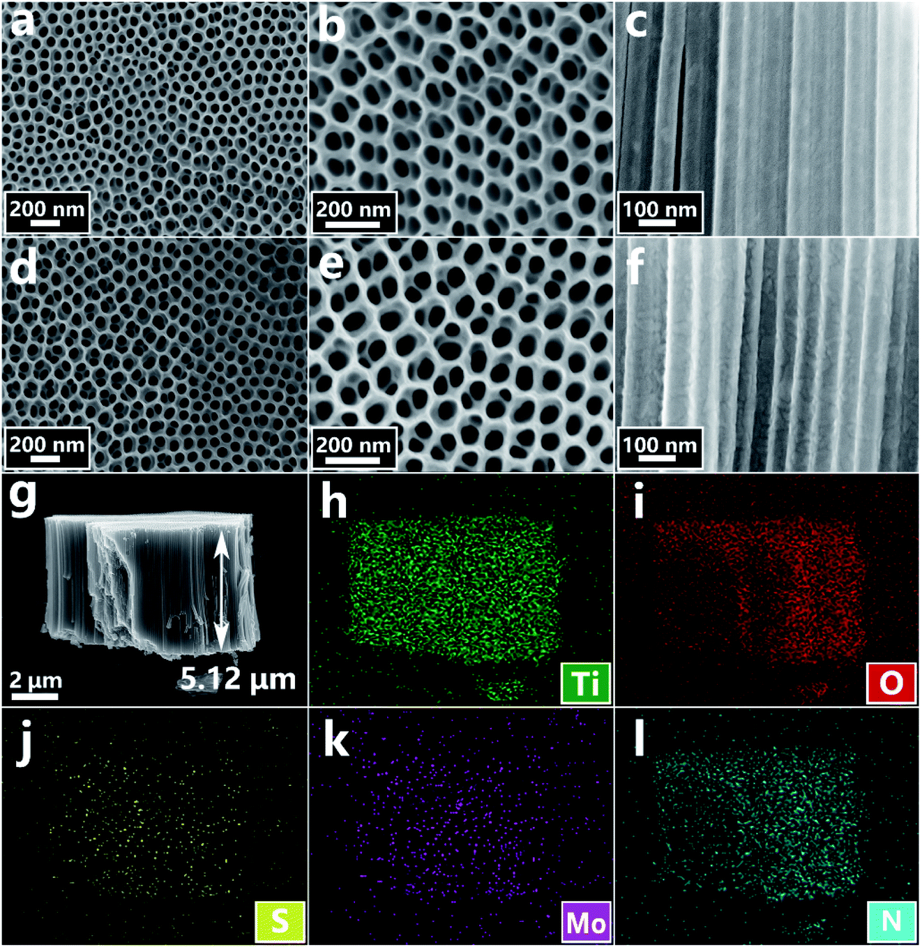 | ||
| Fig. 2 Top-view and cross-sectional FESEM images of (a–c) blank TNTAs and (d–f) T(BM)2 heterostructure, (g) low-magnification FESEM image with corresponding (h–l) elemental mapping results. | ||
To obtain more enriched information on the microscopic structures of the samples, transmission electron microscopy (TEM) measurements were performed. As displayed in Fig. 3a and S10a,† pristine TNTAs feature a uniform and nanotubular structure and this agrees well with the FESEM results (Fig. 2). Fig. 3c shows that an ultra-thin BPEI layer with a thickness of ca. 0.8 nm was closely wrapped on the surface of the TNTA substrate. Meanwhile, as revealed by the TEM images of T(BM)2 in Fig. 3c and d and S10c and d,† MoS2 QDs are evenly distributed on the BPEI-encapsulated TNTA scaffold as marked by the yellow circles, indicating that MoS2 QDs were electrostatically deposited on the TNTAs with the assistance of BPEI by way of the LbL assembly buildup. Consistently, the HRTEM image of T(BM)2 (Fig. 3d) demonstrates two sets of distinct lattice fringes of 0.35 and 0.27 nm, corresponding to the (101) and (100) crystal planes of anatase TiO2 (Fig. 3b) and MoS2 QDs, respectively. Thus uniform encapsulation of TNTAs with BPEI and distribution of MoS2 QDs on the TNTAs can be evidenced by the TEM elemental mapping results [Fig. 3e–j] and EDS results (Fig. S11†), wherein the N signal stems from the BPEI layer and Mo & S signals originate from MoS2 QDs, verifying the formation of distinguishable and intimate interfaces among the ultra-thin BPEI layer, MoS2 QDs and TNTA scaffold, which would facilitate the interfacial charge separation and transfer.
 | ||
| Fig. 3 TEM and HRTEM images of (a and b) TNTAs and (c and d) T(BM)2, (e) TEM image of T(BM)2 with corresponding (f–j) elemental mapping results. Insets in (b and d) are the corresponding HRTEM images and insets in (a and c) are the schematic models. | ||
3.2. PEC water splitting performances
PEC water splitting performances of the samples were systematically probed to evaluate the role of cooperativity between the ultra-thin BPEI layer and MoS2 QDs in affecting the separation and transfer of photoinduced charge carriers over multilayered photoanodes. The influence of MoS2 QD loading amount and assembly bilayer number on the PEC water splitting performances of T(BM)n multilayered heterostructures was firstly explored. As shown in Fig. S12,† the MoS2 QD loading amount affects the photocurrent of T(B–M)n heterostructures under simulated solar light irradiation. Notably, the loading amount of MoS2 QDs on the TNTA framework was controlled by the concentration of MoS2 QDs used during the LbL assembly buildup. Specifically, the PEC performance of T(BM)n is closely related to the MoS2 QD concentration and it increases with boosting the MoS2 QD concentration from 12.5 to 25 mg L−1 and then it decreases with additionally increasing the concentration to 50 mg L−1, based on which the optimal concentration of MoS2 QD aqueous solution used is determined to be 25 mg L−1. Normally, over-deposition of MoS2 QDs induces their agglomeration, which may reduce the active site number, thus retarding the interfacial charge transfer. Moreover, as displayed in Fig. S13,† photocurrents of T(BM)n (n = 1, 2, 4, 6, 8) multilayered heterostructures in the I–t and LSV results are closely associated with the number of assembly bilayers, that is, photocurrent increases gradually with boosting the number of assembly bilayers from one to two and then it decreases upon further increasing the number of assembly bilayers to eight, based on which the optimal assembly bilayer number was determined to be two. This result is reasonable since more BPEI and MoS2 QDs were deposited on the TNTA surface with considerably increasing the assembly bilayer number, thereby causing the unfavorable agglomeration, shielding the active sites on the MoS2 QDs, and reducing the photocurrent. Additionally, as reflected by Fig. S14,† we found that the deposition time of each bilayer during the LbL assembly exerts negligible influence on the PEC performances of T(BM)n (n = 1, 2, 4, 6, 8) multilayered heterostructures, suggesting that the electrostatic attachment of BPEI and MoS2 QDs on the TNTA substrate rapidly reaches saturation within a short deposition time (1 min). Based on the above analysis, the optimal MoS2 QD concentration (25 mg L−1) and assembly bilayer number (n = 2) during the LbL assembly were determined, that is, T(BM)2, which was used for the following systematic comparison.Fig. 4a shows the linear sweep voltammetry curves (LSV) of different photoanodes under simulated solar light irradiation. It is worth noting that the photocurrent of all these samples is almost zero in the dark and an apparent response was observed under simulated solar light irradiation, indicating that the photocurrent is truly caused by a PEC water splitting process. Apparently, the photocurrent of the samples increases with increasing the bias voltage, indicative of the quintessential n-type semi-conductor.49 Note that the photocurrent of TB2 is 200 μA cm−2 (0.61 V vs. RHE), which is about two times larger than that of blank TNTAs, suggesting that encapsulation of TNTAs with the ultra-thin BPEI layer not only plays a crucial role as a positively charged building block but also boosts the interfacial charge separation/transfer photoexcited over the TNTA substrate. It has been reported that BPEI is able to act as an electron donor and we speculate that the ultra-thin BPEI layer integrated in-between the interface of TNTAs and MoS2 QDs on the entire TNTA scaffold can serve as a high-efficiency hole trap for boosting charge separation. This deduction can be strongly evidenced by the excellent reducing capability of BPEI (Fig. S15†), which enables rapid reduction of the metal precursor to metal nanocrystals merely under ambient conditions. Moreover, it is worth noting that BPEI aqueous solution exhibits no light absorption in the UV and visible regions (Fig. S16†), implying that BPEI demonstrates no light absorption in the solar spectrum and it cannot serve as a photosensitizer, consistent with the DRS results (Fig. 1c). Consequently, the hole-withdrawing role of BPEI in constructing a cascade hole transfer channel to benefit effective charge separation was ascertained, thereby contributing to the markedly enhanced PEC water splitting performances of TB2. It should be noted that the photocurrent of TM2 is higher than that of blank TNTAs to some extent, which highlights the pivotal role of MoS2 QDs in enhancing the charge separation in terms of its excellent electron-transporting capability. Significantly, T(BM)2 displays the most enhanced photocurrent which substantially surpasses the TB2, TM2 and TNTA counterparts and the photocurrent follows the order of T(BM)2 > TB2 > TM2 > TNTAs > Ti(BM)2. Especially, the photocurrent of T(BM)2 is larger than the integrated photocurrents of TB2 and TM2, which persuasively confirms the cooperativity of the ultra-thin BPEI layer and MoS2 QDs in boosting the photocurrent of the T(BM)2 ternary multilayered photoanode. Besides, the almost zero photocurrent of Ti(BM)2 suggests the importance of the TNTA substrate (TiO2) in the composite multilayered photoanode, which was photoexcited under simulated solar light irradiation and no charge carriers were produced once TNTAs were replaced with Ti foil. Based on the LSV results, applied bias photon-to-current efficiency (ABPE) of the photoelectrodes can be calculated using the following formula:50
 | (2) |
 is the standard reversible potential which is 1.23 V vs. RHE, and V is the applied bias potential vs. RHE. As revealed in Fig. 4b, T(BM)2 displays the optimal ABPE of 0.16%, followed by TB2, TM2, TNTAs and T(BM)2 with ABPE of 0.09, 0.06, 0.04 and 0%, respectively. Obviously, T(BM)2 exhibits the most enhanced ABPE with respect to other counterparts under the same conditions and this agrees with LSV results.
 | ||
| Fig. 4 (a) LSV results (scan rate: 5 mV s−1) with (b) ABPE results, (c) transient photocurrent responses (I–t) (light on/off cycle: 10 s, bias voltage: 0.61 V vs. RHE), (d) EIS results (with an amplitude of 10 mV in the frequency range of 105 to 0.01 Hz) with (e) Bode plots, (f) OCVD results with (g) average electron lifetime (τn) of T(BM)2, TB2, TM2, TNTAs and Ti(BM)2 under simulated solar light irradiation (AM1.5) in Na2SO4 aqueous solution (pH = 6.69). (h) Mott–Schottky plots of different photoanodes with (i) charge carrier density calculated based on the M–S plots. The inset in (d) demonstrates the equivalent circuit. | ||
Fig. 4c illustrates the on–off transient photocurrent responses of different photoanodes at a bias of 0.61 V RHE under simulated solar light irradiation. Notably, TB2 and TM2 show much higher photocurrent than TNTAs, once again corroborating that the ultra-thin BPEI layer and MoS2 QDs are beneficial for improving the interfacial charge separation. Intriguingly, T(BM)2 still demonstrates the most enhanced photocurrent density relative to TB2, TM2, TNTAs and Ti(BM)2 counterparts, which is in faithful agreement with the LSV (Fig. 4a) and ABPE results (Fig. 4b). The optimal photocurrent of T(BM)2 is mainly ascribed to its unique multilayered nanostructure, wherein periodically alternately deposited ultra-thin BPEI layer and MoS2 QDs serve as efficient hole and electron transfer channels that facilitate spatial charge separation/transfer, respectively. This can be corroborated by probing the photocurrent of the composite photoanode with different stacking fashions (Fig. S17 and S18†) to determine the impact of the interfacial interaction mode between the BPEI layer and MoS2 QDs on the PEC water splitting performances. Specifically, T(BBMM) (Fig. S17b†) and T(MMBB) (Fig. S17c†) counterparts were deliberately designed, wherein two ultra-thin BPEI layers were firstly deposited on the TNTA surface followed by deposition of two more layers of MoS2 QDs rather than being alternately deposited as observed in T(BM)2. In other words, the TNTA substrate was fully encapsulated by the BPEI layer and then MoS2 QDs were all electrostatically assembled on the outer surface. Fig. S18† shows that T(BBMM) and T(MMBB) exhibit inferior photocurrent to T(BM)2, indicative of the paramount importance of alternately depositing the BPEI layer and MoS2 QDs in a face-to-face stacking way for accelerating the interfacial charge transfer rate. The result highlights the advantage of the LbL assembly in boosting interfacial charge transfer efficiency compared to the irregularly and randomly integrated self-assembly approach. Based on the above control experiments, we can speculate that electrons photoexcited from TNTAs are firstly transferred over the ultra-thin BPEI layer whose thickness is remarkably small than the mean free path of electrons and then captured by MoS2 QDs. Simultaneously, holes are efficaciously trapped by the ultra-thin BPEI layer periodically integrated at the interface of MoS2 QDs on the outer surface of TNTAs, thus fulfilling the separation of photo-induced charge carriers. This speculation can be additionally corroborated by another control experiment. As displayed in Fig. S18d and S17d,† PEC performances of T(B2 + M2), which was fabricated by mechanically dipping the TNTA substrate in a mixed aqueous solution containing equivalent MoS2 QDs and BPEI without carefully tuning their surface charge properties, are much lower than that of T(BM)2 under the same conditions, which strongly confirms that the electrostatic self-assembly is indispensable for the LbL assembly of high-efficiency T(BM)n multilayered heterostructures. Additionally, the result also suggests that synergistic interaction of BPEI and MoS2 QDs can be achieved via ingenious and rational interface design for effectively suppressing the recombination of photogenerated electron–hole pairs. The pivotal roles of BPEI and MoS2 QDs in triggering the directional hole and electron transfer were also reflected by the defect-induced PEC performances of TB1 and TM1 under visible light irradiation (λ > 420 nm), as displayed in Fig. S19.†
Electrochemical impedance spectroscopy (EIS) measurements in the dark and under simulated solar light irradiation were further carried out to evaluate the interfacial charge transfer resistance between the photoelectrodes and electrolyte.51 Nyquist plots of the different photoanodes were collected in the dark (Fig. S20†), which suggest that all the photoelectrodes exhibit quite large charge transfer resistance Rct, suggesting that the charge transfer efficiency in the interfacial region is relatively low in the dark without the involvement of photo-induced charge carriers. Nevertheless, it should be particularly noted that the charge transfer efficiency of these electrodes without light irradiation determined from the semicircular arc radius follows the same order as that of LSV and I–t results, i.e., T(BM)2 > TB2 > TM2 > TNTAs. The result implies that BPEI encapsulation and MoS2 QD deposition on the TNTA framework enabled by the LbL assembly approach as well as their cooperativity indeed favor reducing the interfacial charge transfer resistance although photo-induced charge carriers are not responsible for the process. As shown in Fig. 4d and simulated EIS results in Table S3,† both TB2 (1211 ohm) and TM2 (2963 ohm) photoanodes exhibited much lower charge transfer resistance (Rct) under simulated solar light illumination relative to TNTAs (3037 ohm). More significantly, T(BM)2 shows the smallest semicircular arc radius compared to other counterparts, which indicates that interfacial charge transport resistance is greatly reduced over T(BM)2 as a result of simultaneous BPEI encapsulation and MoS2 QDs deposition via the LbL assembly, thereby causing a dramatic drop in Rct (786 ohm) and improved charge separation efficiency as well as PEC water splitting performances. Furthermore, EIS results were analyzed to assess the charge lifetime from the perspective of interfacial resistance. Electron lifetime (τ) can be estimated by using the following formula:16
| τrel = 1/(2πfmax) | (3) |
Open-circuit voltage decay (OCVD) measurements were performed by irradiating the photoelectrode at open circuit potential and then monitoring the decay of the voltage with time upon switching off the light irradiation.52 OCVD analysis has been well-established as a simple and efficacious technique to determine the charge decay kinetics especially the electron lifetime (τn). As displayed in Fig. 4f, the open-circuit voltage (Voc) of the electrode substantially increases arising from instant production of a great number of charge carriers on the photoanode under simulated solar light irradiation and then it gradually decreases and decays to the lower Voc once the light irradiation is turned off, based on which charge separation efficiency can be evaluated. The average electron lifetime (τn) was determined according to the formula given below:31
| τn = kBT/e(dVoc/dt)−1 | (4) |
Mott–Schottky (M–S) results of the photoelectrodes were analyzed to evaluate the charge carrier density. Fig. 4h shows the Mott–Schottky (M–S) plots of the different photoanodes, in which slopes of the linear part of the curves are positive, indicating n-type semiconductors, consistent with the LSV results (Fig. 4a). Charge carrier density ND of the different photoelectrodes was determined from Fig. 4h using the following equation:4
 | (5) |
With a view to unlocking the influence of PE on the PEC water splitting performances, photocurrents of T(PE–M)n under simulated solar light irradiation were probed, in which BPEI was replaced with other positively charged PEs. As displayed in Fig. S21a and b,† the photocurrent of T(PE–M)n (PE = BPEI, PAH, PDDA; n = 1) follows a descending order of T(BPEI–M)1 > T(PAH–M)1 > T(PDDA–M)1 > TNTAs. Virtually, there has been no report on the role of PEs in shuttling and transferring the charge carriers considering their polymeric properties.5,54 However, our results undoubtedly evidence that BPEI outperforms other PE counterparts as a hole transfer mediator to promote directional hole transport. Besides, the MoS2 QD ingredient in T(BM)2 was replaced with the negatively charged PE of PSS to objectively evaluate the contributing role of MoS2 QDs in the PEC water splitting reaction. As reflected by Fig. 5a and b, the photocurrent of T(B–PSS)2 under simulated solar light irradiation was lower than that of T(BM)2, which highlights the imperative role of MoS2 QDs in helping to construct a cascade electron transport channel. This speculation can be further substantiated by comparing the photocurrent of T(BM)2 with TB2 with the same deposition amount of BPEI, for which T(BM)2 demonstrates considerably enhanced photocurrent relative to TB2, once again confirming that the MoS2 QDs alternately deposited on the TNTA surface indeed contribute to the photocurrent enhancement of T(BM)2 by acting as the interfacial electron transfer mediator. In this regard, it is the simultaneously built-in electron and hole transfer channels in the multilayered photoanodes enabled by the LbL assembly that ultimately result in the markedly enhanced PEC water splitting performances of T(BM)2.
 | ||
| Fig. 5 (a and b) On–off transient photocurrent and LSV results (scan rate: 5 mV s−1, bias voltage: 0.61 V vs. RHE) of TNTAs, T(BM)2 and T(B–PSS)2 in Na2SO4 aqueous solution (pH = 6.69) under simulated solar light irradiation (AM1.5), (c) IPCE results and (d) PL spectra of T(BM)2, TB2, TM2 and TNTAs, (e) LSV results of TNTAs, T(BM)2 and T(BM)2 after dipping in DI H2O for 1 h and 2 h, (f) photocurrent of T(BM)2 under continuous simulated solar light irradiation after adding 0.05 M Na2SO3 in Na2SO4 aqueous solution (pH = 6.69) (bias voltage: 0.61 V vs. RHE). | ||
Incident photon-to-current conversion efficiencies (IPCEs) of the photoanodes were explored to uncover the light-responsive region that is responsible for the significantly enhanced PEC water splitting performances of T(BM)2. IPCE is defined by the following equation:55
 | (6) |
It has been well-established that photoluminescence (PL) spectra can be utilized to evaluate the separation efficiency of photo-generated electron–hole pairs over the semiconductor. As shown in Fig. 5d, the PL spectrum of anatase TiO2 (TNTAs) mainly includes three physical modes, i.e., self-trapped excitons, oxygen vacancies, and surface states.56 The peak at ca. 420 nm is ascribed to the self-trapped excitons of anatase TiO2 from the TNTA substrate and the PL intensity of this peak for TNTAs, TM2, TB2, and T(BM)2 successively decreases and follows the order of T(BM)2 < TB2 < TM2 < TNTAs, suggesting that T(BM)2 demonstrates the lowest recombination rate of electron–hole pairs, thereby leading to the optimal PEC water splitting performances. It is worth noting that PL results are in line with PEC performances.
Photostability is a paramount sector of photoanodes for future practical application. PEC water splitting performances of T(BM)2 under simulated solar light irradiation were probed under continuous solar light irradiation for 2 h. As displayed in Fig. S22,† T(BM)2 demonstrates unfavorable photostability under continuous simulated solar light irradiation. This might be ascribed to the dissolution of BPEI in the electrolyte or, probably, consumption of BPEI by holes during the PEC water splitting process, thus leading to disintegration of the multilayered nanostructure of T(BM)2. In this regard, with a view to unveiling the reasons, PEC performances of T(BM)2 after being dipped in the electrolyte (Na2SO4) for the designated time (1 h/2 h) were explored and compared with those of freshly prepared T(BM)2. Fig. 5e and S23† shows that PEC performances (LSV & I–t) of T(BM)2 dipped in the electrolyte (Na2SO4) for 1 & 2 h were almost analogous to that of the freshly prepared counterpart, which excludes the dissolution of the ultra-thin BPEI layer in T(BM)2 in the electrolyte (Na2SO4). On the other hand, it should be noted that BPEI is a branched polymer and features an ultra-long molecular chain with a large molecular weight (25 kDa), which makes the complete consumption of BPEI by holes impossible. Consequently, slow charge transport kinetics especially the interfacial hole transfer kinetics is the core factor influencing the photostability of T(BM)2 for PEC water oxidation, for which the holes produced over the T(BM)2 photoanode might oxidize the MoS2 QDs, thereby deteriorating the photostability. Furthermore, XPS results of T(BM)2 after continuous simulated solar light irradiation (2 h) were analyzed. As revealed in Fig. S24,† no apparent B.E. shifts were observed in the high-resolution N 1s spectra of T(BM)2 after continuous light irradiation in comparison with those of freshly prepared T(BM)2, thereby substantiating that the ultra-thin BPEI layer was retained during the continuous simulated solar light irradiation, confirming the favorable photostability of T(BM)2. To corroborate this speculation, a minute amount of hole scavenger (Na2SO3) was added into the electrolyte (Na2SO4) to expedite the interfacial hole transfer kinetics and reduce energy loss in the water oxidation reaction, by which nearly 100% hole injection efficiency was achieved.57Fig. 5f shows the photocurrent of T(BM)2 in Na2SO4 (Na2SO3) under consecutive simulated solar light irradiation for 2 h, from which it is clearly seen that T(BM)2 demonstrates favorable photostability, distinct from the result probed in the pristine electrolyte (Na2SO4). Consistently, as shown in Fig. S25,† the FTIR spectrum of T(BM)2 after continuous light irradiation is same as that of pristine T(BM)2 with the peak intensity and position of typical functional groups from BPEI retained, verifying the structural integrity and favorable photostability of T(BM)2. The result also corroborates that hole is the origin leading to the poor photostability of T(BM)2 and it is of paramount importance to finely tune the interfacial hole transfer to avoid its direct oxidation to the MoS2 QD ingredient.
3.3. PEC water dissociation mechanism
On the basis of the above systematic investigation, a feasible PEC water splitting mechanism of T(BM)n was tentatively proposed. As depicted in Scheme 2, when T(BM)2 was irradiated by simulated solar light, the TNTA substrate (TiO2) was instantly photoexcited to produce the electron–hole pairs with electrons photoexcited to the conduction band (CB), meanwhile leaving holes in the valence band (VB). Considering the uniform and intimate BPEI encapsulation on the whole TNTA framework in the T(BM)2, the transfer speed of holes accumulated in the VB of TiO2 was remarkably expedited in terms of the strong reducing capability of BPEI, which is able to serve as an efficacious hole transfer mediator to promote the directional hole transport for water oxidation. Simultaneously, the MoS2 QD ingredient in the T(BM)2 plays an indispensable role in accelerating the unidirectional electron transport from the CB of TiO2 and provides abundant active sites for H2 evolution as a result of the quantum confinement effect. Alternatively, it should be emphasized that the ultra-thin BPEI layer and MoS2 QD building blocks were periodically alternately stacked on the TNTA surface; (BPEI/MoS2 QDs) bilayer assembly units integrated in the T(BM)n multilayered photoanode constitute spatially separated cascade charge transfer channels, wherein the periodic ultra-thin BPEI layer forms the hole transfer channel and the MoS2 QD layer serves as the electron transfer channel. Hence, holes transferred by the ultra-thin BPEI layer enables the oxidation of water to oxygen at the photoanode and electrons migrated by the MoS2 QD layer are directed to the external circuit to reduce water to hydrogen at the photocathode, thus synergistically resulting in the considerably enhanced separation and prolonged lifetime of charge carriers. Besides, the 1D nano-architecture of TNTAs also contributes partially to the rapid charge transport in terms of its unique structural merits.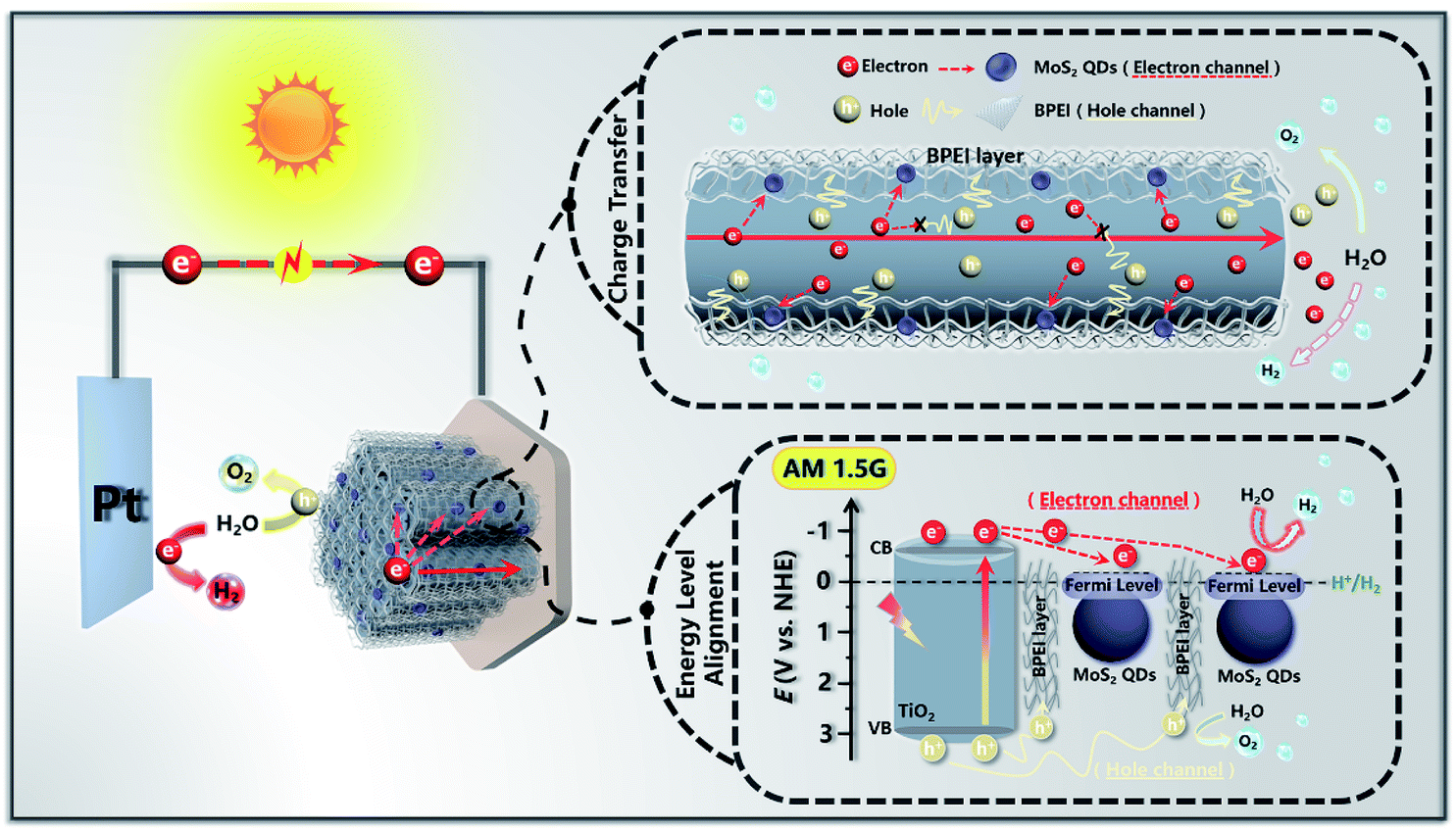 | ||
| Scheme 2 Schematic diagram illustrating the PEC water splitting mechanism of the T(BM)2 ternary multilayered heterostructure. | ||
4. Conclusions
In summary, spatially hierarchically ordered T(BM)n ternary photoanodes were exquisitely designed by a facile and green LbL assembly strategy based on the pronounced electrostatic interaction, in which the ultra-thin BPEI layer and MoS2 QD building blocks were alternately and intimately integrated in a face-to-face stacking fashion on the TNTA surface. The periodically alternately deposited BPEI and MoS2 QD layers serve as high-efficiency hole and electron transfer channels in the light of the strong reducing and electron-transferring capabilities of BPEI and MoS2 QDs, which are beneficial for rapid and directional hole and electron transfer for the charge carrier photoexcited over TNTAs, ultimately giving rise to the significantly boosted PEC water spitting performances of T(BM)n multilayered photoanodes under simulated solar light irradiation, substantially outperforming the single and binary counterparts. More intriguingly, PEC water splitting performances of T(BM)n heterostructures can be finely tuned by the assembly fashion and assembly bilayer number. The cooperative synergy arising from the alternate integration of the ultra-thin BPEI layer and MoS2 QDs on the TNTA framework enabled by the LbL assembly is responsible for the substantial PEC water splitting performance enhancement, based on which a feasible PEC water splitting mechanism of T(BM)n was presented. It is hoped that our work would provide new insights on the promising potential of polymers in mediating spatial charge transfer/separation and meanwhile, inspire more sparkling ideas for rationally constructing multilayered photoelectrodes for solar energy conversion.Conflicts of interest
There are no conflicts to declare.Acknowledgements
The support by the award Program for Minjiang scholar professorship is greatly acknowledged. This work was financially supported by the National Natural Science Foundation of China (No. 21703038).Notes and references
- M. G. Walter, E. L. Warren, J. R. McKone, S. W. Boettcher, Q. Mi, E. A. Santori and N. S. Lewis, Chem. Rev., 2010, 110, 6446–6473 CrossRef CAS.
- A. Fujishima and K. Honda, Nature, 1972, 238, 37–38 CrossRef CAS PubMed.
- T. Hisatomi, J. Kubota and K. Domen, Chem. Soc. Rev., 2014, 43, 7520–7535 RSC.
- Z. Zhang and P. Wang, Energy Environ. Sci., 2012, 5, 6506 RSC.
- Z. L. Wang, Adv. Mater., 2003, 15, 432–436 CrossRef CAS.
- F.-X. Xiao and B. Liu, Adv. Mater. Interfaces, 2018, 5, 1701098 CrossRef.
- Z. Liu, X. Zhang, S. Nishimoto, M. Jin, D. A. Tryk, T. Murakami and A. Fujishima, J. Phys. Chem. C, 2008, 112, 253–259 CrossRef CAS.
- F. X. Xiao, ACS Appl. Mater. Interfaces, 2012, 4, 7055–7063 CrossRef CAS PubMed.
- F. X. Xiao and B. Liu, Nanoscale, 2017, 9, 17118–17132 RSC.
- K. Lee, A. Mazare and P. Schmuki, Chem. Rev., 2014, 114, 9385–9454 CrossRef CAS PubMed.
- J. Zhang, G. Xiao, F.-X. Xiao and B. Liu, Mater. Chem. Front., 2017, 1, 231–250 RSC.
- T.-S. Kang, A. P. Smith, B. E. Taylor and M. F. Durstock, Nano Lett., 2009, 9, 601–606 CrossRef CAS.
- Y. Hou, X. Li, Q. Zhao, X. Quan and G. Chen, J. Mater. Chem., 2011, 21, 18067 RSC.
- T. Li, Y.-B. Li, X.-C. Dai, M.-H. Huang, Y. He, G. Xiao and F.-X. Xiao, J. Phys. Chem. C, 2019, 123, 4701–4714 CrossRef CAS.
- K.-Y. Jiang, X.-C. Dai, Y. Yu, Q.-L. Mo and F.-X. Xiao, J. Phys. Chem. C, 2018, 122, 12291–12306 CrossRef CAS.
- X.-C. Dai, M.-H. Huang, Y.-B. Li, T. Li, B.-B. Zhang, Y. He, G. Xiao and F.-X. Xiao, J. Mater. Chem. A, 2019, 7, 2741–2753 RSC.
- J. H. Park, S. Kim and A. J. Bard, Nano Lett., 2006, 6, 24–28 CrossRef CAS.
- M. Ge, J. Cai, J. Iocozzia, C. Cao, J. Huang, X. Zhang, J. Shen, S. Wang, S. Zhang, K.-Q. Zhang, Y. Lai and Z. Lin, Int. J. Hypertens., 2017, 42, 8418–8449 CAS.
- S. Zhang, Y. S. Park, J. Li, X. Lu, W. Zhang and X. Zhang, Phys. Rev. Lett., 2009, 102, 023901 CrossRef.
- C. Ratanatawanate, A. Chyao and K. J. Balkus, Jr., J. Am. Chem. Soc., 2011, 133, 3492–3497 CrossRef CAS.
- X.-F. Gao, H.-B. Li, W.-T. Sun, Q. Chen, F.-Q. Tang and L.-M. Peng, J. Phys. Chem. C, 2009, 113, 7531–7535 CrossRef CAS.
- Y. Hou, X. Li, X. Zou, X. Quan and G. Chen, Environ. Sci. Technol., 2009, 43, 858–863 CrossRef CAS.
- L. Hou, S. Li, Y. Lin, D. Wang and T. Xie, J. Colloid Interface Sci., 2016, 464, 96–102 CrossRef CAS.
- M. Wang, L. Sun, Z. Lin, J. Cai, K. Xie and C. Lin, Energy Environ. Sci., 2013, 6, 1211 RSC.
- M.-Z. Ge, S.-H. Li, J.-Y. Huang, K.-Q. Zhang, S. S. Al-Deyab and Y.-K. Lai, J. Mater. Chem. A, 2015, 3, 3491–3499 RSC.
- Z. Zeng, F.-X. Xiao, H. Phan, S. Chen, Z. Yu, R. Wang, T.-Q. Nguyen and T. T. Yang Tan, J. Mater. Chem. A, 2018, 6, 1700–1713 RSC.
- X. Chen and C. Burda, J. Am. Chem. Soc., 2008, 130, 5018–5019 CrossRef CAS.
- S. U. M. Khan, M. Al-Shahry and W. B. Ingler, Science, 2002, 297, 2243 CrossRef CAS.
- Z. Zeng, Z. Yin, X. Huang, H. Li, Q. He, G. Lu, F. Boey and H. Zhang, Angew. Chem., Int. Ed., 2011, 50, 11093–11097 CrossRef CAS.
- F. X. Xiao, M. Pagliaro, Y. J. Xu and B. Liu, Chem. Soc. Rev., 2016, 45, 3088–3121 RSC.
- Z. Zeng, F.-X. Xiao, X. Gui, R. Wang, B. Liu and T. T. Yang Tan, J. Mater. Chem. A, 2016, 4, 16383–16393 RSC.
- Z. Zeng, T. Li, Y.-B. Li, X.-C. Dai, M.-H. Huang, Y. He, G. Xiao and F.-X. Xiao, J. Mater. Chem. A, 2018, 6, 24686–24692 RSC.
- D. Kim, M. Gu, M. Park, T. Kim and B.-S. Kim, Mol. Syst. Des. Eng., 2019, 4, 65–77 RSC.
- X. Ren, L. Pang, Y. Zhang, X. Ren, H. Fan and S. Liu, J. Mater. Chem. A, 2015, 3, 10693–10697 RSC.
- C. Kormann, D. W. Bahnemann and M. R. Hoffmann, J. Phys. Chem., 1988, 92, 5196–5201 CrossRef CAS.
- F. X. Xiao, J. Miao and B. Liu, J. Am. Chem. Soc., 2014, 136, 1559–1569 CrossRef CAS.
- F. X. Xiao, S. F. Hung, J. Miao, H. Y. Wang, H. Yang and B. Liu, Small, 2015, 11, 554–567 CrossRef CAS.
- N. Nakayama and T. Hayashi, Colloids Surf., A, 2008, 317, 543–550 CrossRef CAS.
- M. R. Nabid, Y. Bide, M. Shojaipour and F. Dastar, Catal. Lett., 2016, 146, 229–237 CrossRef CAS.
- F. Kretschmer, U. Mansfeld, S. Hoeppener, M. D. Hager and U. S. Schubert, Chem. Commun. (Cambridge, U. K.), 2014, 50, 88–90 RSC.
- Y. Dong, R. Wang, H. Li, J. Shao, Y. Chi, X. Lin and G. Chen, Carbon, 2012, 50, 2810–2815 CrossRef CAS.
- F. X. Xiao, Z. Zeng and B. Liu, J. Am. Chem. Soc., 2015, 137, 10735–10744 CrossRef CAS.
- Z. Zeng, Y.-B. Li, S. Chen, P. Chen and F.-X. Xiao, J. Mater. Chem. A, 2018, 6, 11154–11162 RSC.
- Q. Quan, S. Xie, B. Weng, Y. Wang and Y.-J. Xu, Small, 2018, 14, 1870096 CrossRef.
- C. Zhang, L. Chen, L. Tan, X. Zheng and Y. Wang, React. Funct. Polym., 2015, 93, 190–201 CrossRef CAS.
- W. Cheng, C. Yang, X. Ding, A. C. Engler, J. L. Hedrick and Y. Y. Yang, Biomacromolecules, 2015, 16, 1967–1977 CrossRef CAS PubMed.
- Q. Wang, J. Huang, H. Sun, Y. H. Ng, K. Q. Zhang and Y. Lai, ChemSusChem, 2018, 11, 1708–1721 CrossRef CAS.
- Y.-B. Li, T. Li, X.-C. Dai, M.-H. Huang, Y. He, G. Xiao and F.-X. Xiao, J. Mater. Chem. A, 2019, 7, 8938–8951 RSC.
- F.-X. Xiao, J. Miao and B. Liu, Mater. Horiz., 2014, 1, 259–263 RSC.
- S.-F. Hung, F.-X. Xiao, Y.-Y. Hsu, N.-T. Suen, H.-B. Yang, H. M. Chen and B. Liu, Adv. Energy Mater., 2016, 6, 1501339 CrossRef.
- J. Bisquert, A. Zaban, M. Greenshtein and I. Mora-Seró, J. Am. Chem. Soc., 2004, 126, 13550–13559 CrossRef CAS.
- A. Zaban, M. Greenshtein and J. Bisquert, ChemPhysChem, 2003, 4, 859–864 CrossRef CAS PubMed.
- P. K. Ghosh and M. E. Azimi, IEEE Trans. Dielectr. Electr. Insul., 1994, 1, 975–981 CrossRef.
- Y.-G. Guo, L.-J. Wan and C.-L. Bai, J. Phys. Chem. B, 2003, 107, 5441–5444 CrossRef CAS.
- S. J. Hong, S. Lee, J. S. Jang and J. S. Lee, Energy Environ. Sci., 2011, 4, 1781 RSC.
- A. K. L. Sajjad, S. Shamaila, B. Tian, F. Chen and J. Zhang, Appl. Catal., B, 2009, 91, 397–405 CrossRef CAS.
- M. Liao, J. Feng, W. Luo, Z. Wang, J. Zhang, Z. Li, T. Yu and Z. Zou, Adv. Funct. Mater., 2012, 22, 3066–3074 CrossRef CAS.
Footnote |
| † Electronic supplementary information (ESI) available. See DOI: 10.1039/c9ta11579j |
| This journal is © The Royal Society of Chemistry 2020 |