A type-II GaSe/GeS heterobilayer with strain enhanced photovoltaic properties and external electric field effects†
Bin
Zhou
a,
Shi-Jing
Gong
 *b,
Kai
Jiang
a,
Liping
Xu
a,
Liyan
Shang
a,
Jinzhong
Zhang
 a,
Zhigao
Hu
 *acd and
Junhao
Chu
acd
aTechnical Center for Multifunctional Magneto-Optical Spectroscopy (Shanghai), Department of Materials, School of Physics and Electronic Science, East China Normal University, Shanghai 200241, China. E-mail: sjgong@ee.ecnu.edu.cn; zghu@ee.ecnu.edu.cn; Fax: +86-21-54342933; Tel: +86-21-54345150
bKey Laboratory of Polar Materials and Devices (MOE), East China Normal University, Shanghai 200241, China
cCollaborative Innovation Center of Extreme Optics, Shanxi University, Taiyuan, Shanxi 030006, China
dShanghai Institute of Intelligent Electronics & Systems, Fudan University, Shanghai 200433, China
First published on 30th October 2019
Abstract
Constructing two dimensional (2D) van der Waals (vdW) heterostructures and understanding their electronic properties are pivotal for developing novel electronic devices. In this work, by using the first-principles calculations, we theoretically demonstrate that the 2D GaSe/GeS van der Waals (vdW) heterobilayer is a robust type-II band alignment semiconductor with a direct band gap of 1.8 eV. It exhibits a remarkable absorbance coefficient of ∼105 cm−1 from the UV to visible light region and a high carrier mobility with anisotropic character. The photoelectric conversion efficiency (PCE) shows a tremendous enhancement under external strain, and shows an efficiency of up to ∼16.8% at 2% compressive strain. Besides, we find that applying an external electric field can effectively modulate its band gap and band offset. Interestingly, a larger external electric field can induce nearly free electron (NFE) states around the conduction band minimum (CBM) in the GaSe/GeS heterobilayer, which leads to the band transition from a semiconductor to metallic status. These results indicate that 2D GaSe/GeS heterostructures will have widespread application prospects in future photovoltaic and optoelectric nanodevices.
1 Introduction
In recent decades, many two dimensional (2D) materials beyond graphene have been extensively studied, which display potential application prospects in the field of photodetectors, field-effect transistors (FETs) and spintronics, due to their distinct electronic properties.1–4 However, it is found that no single 2D material possesses perfect properties that meet the requirements of practical applications. Recently, stacking vertically atomic thickness van der Waals (vdW) heterostructures has been confirmed to be a powerful strategy to leverage and combine the optoelectronic characteristics of different 2D materials in experiment and theory.5–8 The 2D heterostructures, in which vdW interactions integrate different 2D materials without considering the crystal lattice mismatch, possess many tailed electronic properties that far outstripped the properties in a single component.9 The 2D heterostructure based layered materials are considered to be good candidate materials for next-generation solar cells.10 However, the photovoltaic efficiency of 2D heterostructure based solar cells displayed is still not ideal and needs extremely urgent improvement.As one member of group IIIA metal monochalcogenides MX (M = Ga, In; X = S, Se, Te), the layered gallium selenide (GaSe) stacking in a Se–Ga–Ga–Se sequence has attracted growing attention due to its superior optoelectronic properties in recent years.11,12 The GaSe crystal has a layered hexagonal structure with strong intralayer and relatively weak interlayer interactions. The monolayer GaSe can be achieved by repeatedly peeling the bulk material, which is called a micromechanical cleavage technique and it has been proven to be a convenient and efficient way to produce high quality and large size single and few layer nanosheets. So far, many optoelectronic devices based on GaSe nanosheets have been successfully fabricated.13–17 For example, D. J. Late et al.13 demonstrated the fabricated field effect transistors (FETs) based on the monolayer GaSe with ON/OFF current ratios up to 105. Hu et al. reported that GaS nanosheet based photodetectors exhibit a superhigh photoresponsivity up to 19.2 A W−1, which is much higher than that of graphene, MoS2 and other 2D semiconductors.14
Additionally, germanium monochalcogenides (GeS, GeSe), which are similar to black phosphorus, have also attracted a lot of research interest since their successful synthesis in experiment.18,19 Single layer GeS has been theoretically predicted to possess a high carrier mobility (∼103 cm2 V−1 s−1) with a suitable band gap value (1.65 eV), which shows promising applications in nanodevices.20–22 It is reported that the 2D GeS monolayer has been achieved experimentally by liquid phase exfoliation recently,23 which paves the way for fabricating the GeS based vdW heterostructure.
In this work, we construct the GaSe/GeS vdW heterostructure and investigate the combined electronic properties. Our attention was mainly focused on the band alignment, optical properties, carrier mobility and electronic field (E-field) effects. The results show that the GaSe/GeS heterobilayer possesses typical type-II band alignment with a direct band gap. Surprisingly, a larger external electric field can induce near free electron (NFE) states24,25 around the conduction band minimum (CBM), which leads to the transition from a semiconductor to metallic status. The present results demonstrate that the GaSe/GeS heterobilayer may become a promising candidate material in applications of nanoelectronic devices.
2 Computational details
First-principles calculations were performed based on density functional theory (DFT), using the projector augmented-wave method as implemented in the Vienna Ab initio Simulation Package (VASP) code.26–28 The exchange correlation functional was used within the generalized gradient approximation of Perdew, Burke and Ernzerhof.29,30 A plane-wave basis set with a cutoff of 500 eV was used and a k mesh of 20 × 5 × 1 was adopted to sample the first Brillouin zone of the monolayers and heterostructure. The conjugate-gradient scheme is used for geometric optimization until the force on each atom is less than 0.01 eV Å−1, and the total energy change is less than 10−5 eV to acquire good convergence. A sufficient vacuum space (≥25 Å) is used along the z direction (normal to the 2D plane) to avoid periodicity interaction between adjacent images. As the van der Waals interaction cannot be effectively described by the PBE functional, the van der Waals interactions are considered by adding a semi-empirical dispersion potential to the Kohn–Sham DFT energy, through a pair-wise force field following Grimme's DFT-D2 method.31 And optB8832 vdW corrections are also considered for comparison. As we know, the PBE functional is known to underestimate the band gap of semiconductors. Thus, the intrinsic electronic and optical properties of the GaSe/GeS heterobilayer and the corresponding isolated monolayers are calculated using the HSE06 methods with the mixing exchange parameter of 0.25 and screening parameter of 0.2 Å−1. The band properties of the heterostructure under an applied external electric field are calculated with the PBE methods to obtain a variation trend.To quantitatively evaluate the relative stability of the heterostructure, the binding energy (Eb) of GaSe/GeS is calculated by Eb = EGaSe/GeS − (EGaSe + EGeS), where EGaSe/GeS, EGaSe, and EGeS represent the total energies of the GaSe/GeS heterobilayer and GaSe and GeS monolayers, respectively.
As the absorption range of the spectrum is very important in the application of optoelectronic devices, we calculate the optical absorption coefficient by using the following formula:
 | (1) |
 | (2) |
| × 〈μck+eα|μvk〉〈μck+eβ|μvk*〉 | (3) |
Furthermore, we estimated the photoelectric conversion efficiency (PCE) by using Scharber's method,33 which is defined as follows:
 | (4) |
To investigate the electronic transport properties of the GaSe/GeS heterobilayer, we calculated the carrier mobility based on the following expression:34
 | (5) |
 . The El is the deformation potential given by El = ΔE/(Δl/l0), which denotes the shift of the band edges compared to the applied strain. C2D is the in-plane elastic modulus, which can be derived from the formula (E − E0)/S0 = (C2D/2)(Δl/l0)2, where E0 and E are the total energies before and after applying uniaxial strain and S0 is the area of the optimized structure at the equilibrium state.
3 Results and discussion
3.1 Geometric structure and stability of the GaSe/GeS heterobilayer
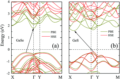
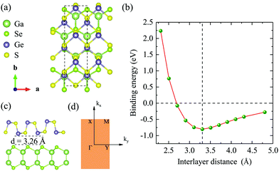
Before studying the 2D GaSe/GeS heterobilayer model, we first investigate the GaSe and GeS monolayers. Based on the minimization of the total energy, we optimize the lattice parameters of the rectangular unit cell GaSe and GeS monolayers. For the rectangular GaSe monolayer, a = 3.84 Å and b = 6.65 Å, and a = 3.66 Å and b = 4.49 Å for the GeS unit cell (see Table 1). The band structures of the GaSe and GeS monolayers are calculated both by PBE and HSE06 functionals, which are plotted together in Fig. 1(a) and (b) for comparison. It is shown that both GaSe and GeS monolayers are indirect band gap semiconductors. The band gap value is 1.82/2.90 eV (PBE/HSE06) for the GaSe monolayer with the conduction band minimum (CBM) being located at the Γ point and the valence band maximum (VBM) between the Γ and X points. The valence band is nearly flat in the central region of the Brillouin zone, which results in very heavy holes. For the GeS monolayer, the band gap is 1.78/2.50 eV with the CBM being located between the Γ and X points and VBM between the Γ and Y points. It is found that the shape of band structures given by two methods is very similar, in which the HSE06 result is almost a linear shift up of the PBE result in band energy. All the results are in good agreement with previous theoretical reports.35,36In order to construct the GaSe/GeS vdW heterobilayer with less lattice mismatch, we construct the GaSe/GeS heterostructure using a 1 × 2 × 1 GaSe rectangular supercell and a 1 × 3 × 1 GeS supercell, as shown in Fig. 2(a) and (c). The lattice mismatch along the x and y directions is less than 3% and 1%, respectively, which are located in a reasonable range, thus a reliable computational result can be achieved. Besides, the stacking pattern effects on the GaSe/GeS vdW heterostructures are also considered, as shown in Fig. S1 (ESI†). The results show that there is little difference in the binding energy between the different stacking configurations. The calculated band structures of two stacking patterns are very similar (see Fig. S2 in the ESI†), thus, we only take one stacking configuration as an example to study the electronic properties of GaSe/GeS heterostructures in this work. The variation of binding energy Eb with the interlayer distance is shown in Fig. 2(b). The minimum binding energy for the heteobilayer is up to 0.8 eV (1.07 eV for optB88) and the equilibrium distance is calculated to be 3.26 Å. The binding energy value, which is about 60 meV per atom, has the same order of magnitude as other typical vdW heterostructures calculated within the same computational scheme (e.g. MoS2/black phosphorus, phosphorene/graphene),37,38 which indicates that the GaSe/GeS vdW heterostructure can be stably formed.
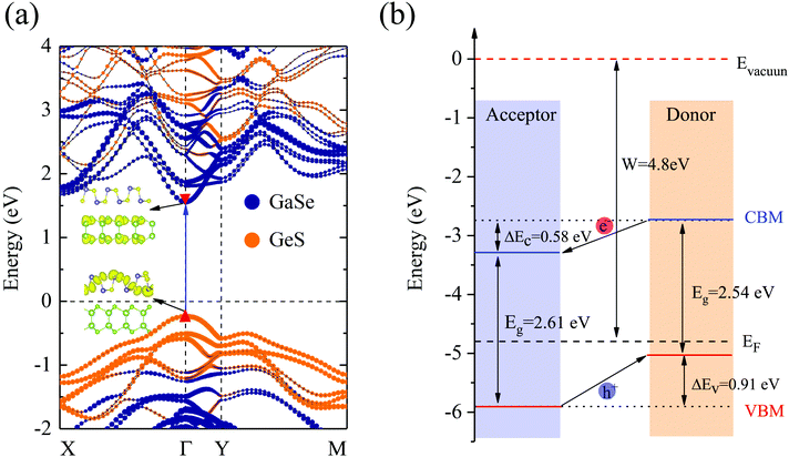
In Fig. 3(a) and (b), we present the projected band structure and band alignment of the GaSe/GeS vdW heterobilayer. It is found that the GaSe/GeS heterobilayer displays semiconductor characteristics with a direct band gap of 1.8 eV (HSE06), in which both the CBM and VBM lie at the Γ point. The CBM and VBM of the GaSe layer are both lower than those of the GeS layer in energy, which forms a staggered type-II band alignment. To further confirm the type II band feature, we also calculated the band-decomposed charge density of the VBM and CBM, as shown in the inset of Fig. 3(a). The lowest-energy electron and hole states are localized on the GaSe layer and GeS layer, respectively. This indicates that the GaSe/GeS heterobilayer is a perfect type-II band alignment semiconductor, which can effectively separate the photogenerated holes and electrons. We have also performed band calculations with optB88 vdW corrections. It is found that different vdW corrections have very small effects on band dispersion and the value of the band gap of the heterostructure (see Fig. S3 in the ESI†). Thus, it can be a good candidate material for optoelectronic applications. In the following discussions, we will use the results from simulations with DFT-D2 corrections. Fig. 3(b) shows the band alignment of the GaSe/GeS heterobilayer, in which the vacuum level (Evacuum) is set as a common energy reference. It is noteworthy that there is a tiny potential difference between the right (GeS) and left (GaSe) vacuum surfaces (see Fig. S4 in the ESI†). This tiny potential step is mainly caused by the dipole moment at the interface due to the charge transfer between layers. As an important factor in designing optoelectronic devices, the band offsets are presented. The valence band offset (VBO) ΔEv and conduction band offset (CBO) ΔEc between the GaSe and GeS layers are calculated to be about 0.91 eV and 0.58 eV, respectively. The larger band offsets can prolong the lifetime of interlayer excitons, which is crucial for improving the efficiency of carrier separation.39 When the GaSe/GeS vdW heterobilayer is exposed to sunlight, the type-II band alignment together with the large band offset ensures the fomation of an interlayer exciton at the lowest energy in the optical spectra,40 thus facilitating the transfer of photogenerated carriers.
The calculated optical absorption coefficient α(ω) as a function of wavelength for the GaSe/GeS heterobilayer and the corresponding monolayers are shown in Fig. 4. The calculated results show that both the GaSe monolayer and GeS monolayer as well as the GaSe/GeS exhibit an absorption coefficient as high as ∼105 cm−1 from the ultraviolet light to visible light range. The optical absorption coefficient of the heterobilayer presents an obvious enhancement compared with the isolated monolayers, which suggests an enhancement of efficiency of solar energy utilization. This is mainly due to overlap of electronic states in the heterostructure caused by the charge transfer and interlayer coupling effects between two constituents.41,42 Besides, the absorption coefficient of monolayer GeS displays anisotropic characteristics in armchair and zigzag directions, while these anisotropic characteristics are weakened in the heterobilayer.
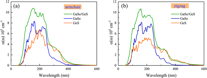 | ||
| Fig. 4 The optical absorption coefficient α(ω) of isolated GaSe and GeS monolayers and the GaSe/GeS heterobilayer along armchair and zigzag directions with the HSE06 method, respectively. | ||
3.2 Carrier mobility of the GaSe/GeS vdW heterobilayer
Based on the deformation potential theory, which is proposed by Bardeen and Shockley,43 we calculated the carrier mobility of 2D GaSe and GeS monolayers as well as the GaSe/GeS heterobilayer at the PBE level, as it has been confirmed to be reliable for carrier mobility prediction.44,45 The calculated carrier mobilities at room temperature (300 K) for the GaSe and GeS monolayers and their heterostructure along the x and y directions are listed in Table 2. The three key parameters, which determine the carrier mobility, i.e., the effective mass m*, deformation potential El and the in-plane stiffness C2D in the propagation direction, are also listed in Table 2. The carrier mobility of 2D GeS shows anisotropic character, in which the mobilities of electrons and holes along the x direction (zigzag direction) are both about 400 cm2 V−1 s−1, while along the y direction (armchair direction), the electron mobility is up to 2253 cm2 V−1 s−1 and hole mobility is about 189 cm2 V−1 s−1. These results are in line with the previously calculated results.46,47 The significant difference between electron mobility and hole mobility could hinder the recombination of photogenerated carriers, thus prolonging the lifetime of carriers.39 For the GaSe monolayer, the electron mobility is up to 583 cm2 V−1 s−1 and 661 cm2 V−1 s−1 along x and y directions, respectively. While the hole mobilities are 216 and 106 cm2 V−1 s−1 for x and y directions, which are found to be close to previous results.45 For the GaSe/GeS heterobilayer, the electron mobility is 661 cm2 V−1 s−1 along the x direction and 583 cm2 V−1 s−1 along the y direction. The hole mobility is 377 cm2 V−1 s−1 along x direction and 193 cm2 V−1 s−1 along y direction. The carrier mobilities are almost a combination of the electron mobility of GaSe and the hole mobility of GeS along the x and y directions. This can be attributed to the CBM and VBM of the heterostructure mainly originating from the GaSe layer and GeS layer, respectively.| Carrier type | m x */m0 | m y */m0 | E lx | E ly | C 2D_x | C 2D_y | μ x | μ y | |
|---|---|---|---|---|---|---|---|---|---|
| GaSe | Electron | 0.24 | 0.17 | 8.29 | 9.40 | 84.88 | 74.62 | 472.30 | 525.48 |
| Hole | 1.33 | 2.08 | 1.94 | 2.07 | 84.88 | 74.62 | 216.11 | 106.70 | |
| GeS | Electron | 0.53 | 0.38 | 3.04 | 1.60 | 46.63 | 14.61 | 426.44 | 2253.51 |
| Hole | 0.25 | 0.27 | 6.00 | 4.82 | 46.63 | 14.61 | 421.58 | 189.52 | |
| GaSe/GeS | Electron | 0.39 | 0.18 | 6.35 | 8.39 | 130.38 | 89.47 | 661.89 | 583.54 |
| Hole | 0.64 | 0.76 | 4.04 | 4.29 | 130.38 | 89.47 | 377.22 | 193.30 |
3.3 Tunable electronic properties and enhanced photoelectric conversion efficiency (PCE) by biaxial and vertical strains
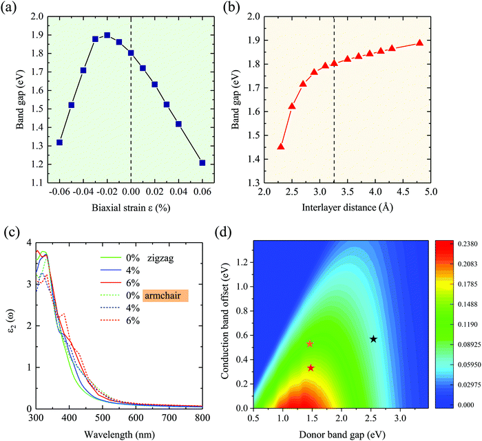
Strain engineering is an effective way to tune the electronic properties of 2D vdW heterostructures. Here, the band gap as a function of biaxial and vertical strains is presented in Fig. 5(a) and (b), in which the effective tunability of the band gap by strain engineering is clearly demonstrated. For the vertical direction, when the compressive strain is applied to the GaSe/GeS heterobilayer, in which the interlayer distance is decreased, the band gap displays a reduced trend. Conversely, when a stretch strain is exerted, a larger interlayer distance will induce an increase of the band gap. Similar behaviors can be found in GeSe/SnS heterobilayers.48 The project band structures under different biaxial and vertical strains are presented in Fig. S5 and S6 (see the ESI†). It is noteworthy that the heterostructures retain type-II band alignment properties, independent of the biaxial and vertical strains. In Fig. 5(c), the optical absorption along the armchair and zigzag directions under biaxial strain is presented. When the strain varies from 0% to +6%, a red shift of the absorption spectrum occurred, which agree with the trend of band gap changing.In addition, following the PCE definition mentioned in computational details, the calculated PCE of the intrinsic GaSe/GeS heterostructures is about 6.1%, which is relatively low for photovoltaic applications. According to Scharber's work, two factors are important to improve the PCE of heterostructures: one is decreasing the CBO, which can increase the Voc, and the other is improving the Jsc by adjusting the band gap of donors Ed. Both factors were involved in modulating the band structure of 2D materials in the heterostructure, which can be realized through applying external strain. The PCE contour plots of the GaSe/GeS heterostructure are shown in Fig. 5(d). It is found that the vertical and biaxial strains could greatly improve the PCE values, which facilitates solar energy utilization. The PCE reaches 11.9% when the interlayer distance decreases to 2.56 Å. While for 2% compressive strain, the PCE can reach as high as 16.8%. The power conversion efficiency is competitive with the theoretical values of many recently proposed 2D heterostructures, such as g-SiC2 (∼12%)49 and MoS2/phosphorene (∼16%).50 The results indicate that the high efficiency of solar energy utilization of GaSe/GeS could be realized by strain engineering, which strikingly broadens its application in optoelectric devices.
3.4 Electric field modulations of the electronic structures in the GaSe/GeS vdW heterobilayer
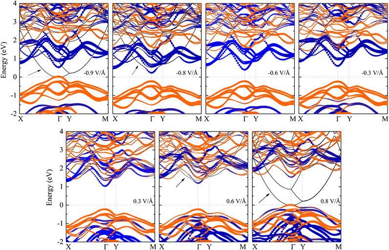
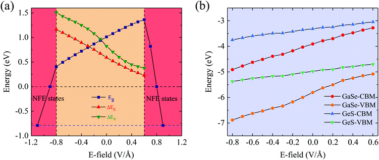
To explore the external E-field effects on the electronic properties of the GaSe/GeS heterobilayer, we consider the E-field direction perpendicular to GaSe/GeS. The positive direction of the E-field is defined as pointing from the GeS layer to the GaSe layer. The projected band structures of the GaSe/GeS heterobilayer with several selected external E-fields are shown in Fig. 6. The GaSe/GeS retains type-II band alignment characteristics under the E-field of −0.8 V Å−1 to 0.6 V Å−1. Interestingly, it is found that extra conduction bands appear near the CBM in the heterostructure, when the applied E-field increases over to Ec = 0.6 V Å−1 (−0.8 V Å−1 for the negative E-field). This phenomenon can be attributed to the electric field induced near free electron (NFE) states in the heterostructure.24,25 The NFE states are not contributed by any electrons around GaSe or GeS layers. The energy level of the NFE bands drops down quickly upon increasing the amplitude of the external E-field. When the applied electric field reaches 0.8 V Å−1 (−0.9 V Å−1), the rapid decline of NFE bands can induce the metallic conducting band structure feature of the GaSe/GeS heterobilayer.The band gap as a function of the external E-field for the GaSe/GeS heterobilayer is shown in Fig. 7(a). Our results show that the band gap can be modulated effectively through the external electric field, which rely on both the intensity and direction of the E-field. When the positive E-field is applied, the band gap increases first, and then starts to decrease rapidly when the E-field strength is beyond 0.6 V Å−1. While the negative E-field is applied, the band gap displays a monotonously decreasing trend. The band gap exhibits a linear modulation effect within Ec (−0.8 V Å−1, 0.6 V Å−1). The band gap is closed when the intensity of the positive (negative) E-field is larger than 0.8(−0.9) V Å−1. Besides, we shift the zero-gap for the hybrid functional according to the band gap differences between PBE and HSE06.25 Thus, the band gap can extend a variety of fitting lines to the HSE06 zero-gap range. The band offsets of the GaSe/GeS heterobilayer that varied with the external E-field are also plotted in Fig. 7(a). We see that both the values of ΔEv and ΔEc exhibit a continuously decreasing trend with the applied E-field changing from −0.8 V Å−1 to 0.6 V Å−1. In Fig. 7(b), we show the evolution of band edges under the external E-field. It can be seen that as the E-field is varied from −0.8 to 0.6 V Å−1, the CBM and VBM of the GaSe layer move upward, while the band edges of the GeS monolayer change little. As the energy of band edges for GeS is always higher than that for the GaSe layer, the heterostructure retains type-II band alignment features in the range of −0.8 V Å−1 to 0.6 V Å−1 for the external E-field. In addition, the GaSe/GeS heterobilayer retains direct band gap features, which is in favour of light absorption. When the applied external electric field reaches −0.8 V Å−1, the band gap decreases to about 1.1 eV (HSE06 level), which is suitable for application in optical absorption within the visible region.
To understand the physical mechanism of charge transfer between GaSe and GeS monolayers under the E-field, we performed the Bader charge analysis.51 The number of transferred electrons between the two layers as a function of the external E-field is shown in Fig. 8(a). When the external E-field is 0 V Å−1, we find that there are net electrons being transferred from the GaSe to GeS layer, and this can be attributed to the built-in E-field along with the direction of the positive external electric field induced by a larger electrostatic potential drop between two layers.52 When the negative E-field is applied gradually, the electrons that are transferred from the GaSe to GeS layer start to decrease, which is due to the reduced net effective internal electric field crossing the interface. When the strength of the external E-field reaches −0.4 V Å−1, the net charges transferred between the two layers are almost zero. As the negative E-field is further increased, the electrons start to transfer from the GeS to GaSe layer. Meanwhile, we also calculate the electrostatic potentials of GaSe/GeS under an external electric field, as shown in Fig. 8(b). With the external electric field increasing from negative to postive, the potential well of GaSe rises up notably, leading to a larger interfacial electrostatic potential difference ΔV. Thus, a stronger interfacial electrostatic field forms, which leads to more charge transfer between GaSe and GeS layers. All the results indicate that the GaSe/GeS heterostructure can be used as a good candidate for next generation optoelectronic devices.
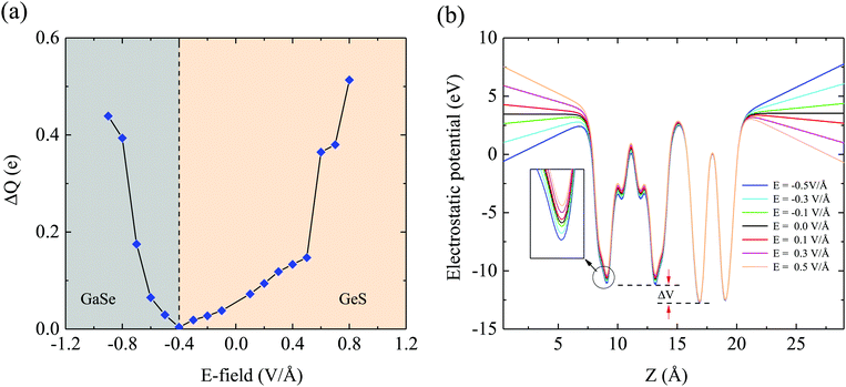 | ||
| Fig. 8 (a) Charge transfer as a function of the external electric field in the GaSe/GeS heterostructure. (b) Electrostatic potentials of GaSe/GeS with different applied electric fields. | ||
4 Conclusions
In summary, by using first-principles calculations, we reveal that the 2D GaSe/GeS vdW heterobilayer is a robust type-II band alignment semiconductor with a direct band gap of 1.8 eV. The heterobilayer shows an excellent absorbance coefficient of ∼105 cm−1 from the UV to visible light range. Meanwhile, the GaSe/GeS heterobilayer possesses a high carrier mobility and displays anisotropic character. The calculated photoelectric conversion efficiency displays a tremendous enhancement under applied external strain, and shows as high as 16.8% at 2% compressive strain. The band gap and band offset of the GaSe/GeS heterobilayer can be effectively modulated through applying a vertical electric field. Moreover, we also find that the GaSe/GeS heterostructure can be transformed into its NFE states under a large electric field. We believe that the theoretical results will shed light on the design and application of novel two-dimensional material-based photovoltaic electronic devices in the future.Conflicts of interest
There are no conflicts to declare.Acknowledgements
The authors would like to thank Dr Wenzhen Dou from Beihang University for constructive discussions. This work was financially supported by the National Natural Science Foundation of China (Grant No. 91833303, 61774058, 61974043, and 61674057), and the National Key R&D Program of China (Grant No. 2017YFA0303403 and 2018YFB0406500), the Projects of Science and Technology Commission of Shanghai Municipality (Grant No. 18JC1412400, 18YF1407200, 18YF1407000, and 19511120100), and the Program for Professor of Special Appointment (Eastern Scholar) at Shanghai Institutions of Higher Learning.References
- S. Z. Butler, S. M. Hollen, L. Cao, Y. Cui, J. A. Gupta, H. R. Gutierrez, T. F. Heinz, S. S. Hong, J. Huang, A. F. Ismach, E. Johnston-Halperin, M. Kuno, V. V. Plashnitsa, R. D. Robinson, R. S. Ruoff, S. Salahuddin, J. Shan, L. Shi, M. G. Spencer, M. Terrones, W. Windl and J. E. Goldberger, ACS Nano, 2013, 7, 2898–2926 CrossRef CAS PubMed.
- G. R. Bhimanapati, Z. Lin, V. Meunier, Y. Jung, J. Cha, S. Das, D. Xiao, Y. Son, M. S. Strano, V. R. Cooper, L. Liang, S. G. Louie, E. Ringe, W. Zhou, S. S. Kim, R. R. Naik, B. G. Sumpter, H. Terrones, F. Xia, Y. Wang, J. Zhu, D. Akinwande, N. Alem, J. A. Schuller, R. E. Schaak, M. Terrones and J. A. Robinson, ACS Nano, 2015, 9, 11509–11539 CrossRef CAS PubMed.
- S. J. Gong, C. Gong, Y. Y. Sun, W. Y. Tong, C. G. Duan, J. H. Chu and X. Zhang, Proc. Natl. Acad. Sci. U. S. A., 2018, 115, 8511–8516 CrossRef CAS PubMed.
- L. P. Xu, P. Zhang, H. Jiang, X. Wang, F. F. Chen, Z. G. Hu, Y. J. Gong, L. Y. Shang, J. J. Zhang, K. Jiang and J. H. Chu, Small, 2019, 1904116 CrossRef CAS.
- A. K. Geim and I. V. J. N. Grigorieva, Nature, 2013, 499, 419 CrossRef CAS.
- K. S. Novoselov, A. Mishchenko, A. Carvalho and A. H. Castro Neto, Science, 2016, 353, aac9439 CrossRef CAS.
- C. Gong and X. Zhang, Science, 2019, 363, 706 CrossRef.
- F. Withers, O. Del Pozo-Zamudio, A. Mishchenko, A. P. Rooney, A. Gholinia, K. Watanabe, T. Taniguchi, S. J. Haigh, A. K. Geim, A. I. Tartakovskii and K. S. Novoselov, Nat. Mater., 2015, 14, 301–306 CrossRef CAS.
- X. Wang and F. Xia, Nat. Mater., 2015, 14, 264–265 CrossRef CAS.
- Q. Xiang, J. Yu and M. Jaroniec, J. Am. Chem. Soc., 2012, 15, 6575–6578 CrossRef.
- W. Feng, W. Zheng, W. W. Cao and P. A. Hu, Adv. Mater., 2014, 26, 6587–6593 CrossRef CAS.
- W. Huang, L. Gan, H. Li, Y. Ma and T. Zhai, CrystEngComm, 2016, 18, 3968–3984 RSC.
- D. J. Late, B. Liu, J. Luo, A. Yan, H. S. Matte, M. Grayson, C. N. Rao and V. P. Dravid, Adv. Mater., 2012, 24, 3549–3554 CrossRef CAS.
- P. Hu, L. Wang, M. Yoon, J. Zhang, W. Feng, X. Wang, Z. Wen, J. C. Idrobo, Y. Miyamoto, D. B. Geohegan and K. Xiao, Nano Lett., 2013, 13, 1649–1654 CrossRef CAS.
- H. Huang, P. Wang, Y. Gao, X. Wang, T. Lin, J. Wang, L. Liao, J. Sun, X. Meng, Z. Huang, X. Chen and J. Chu, Appl. Phys. Lett., 2015, 107, 143112 CrossRef.
- P. Hu, Z. Wen, L. Wang, P. Tan and K. Xiao, ACS Nano, 2012, 6, 5988–5994 CrossRef CAS.
- X. Li, M. W. Lin, J. Lin, B. Huang, A. A. Puretzky, C. Ma, K. Wang, W. Zhou, S. T. Pantelides, M. Chi, I. Kravchenko, J. Fowlkes, C. M. Rouleau, D. B. Geohegan and K. Xiao, Sci. Adv., 2016, 2, e1501882 CrossRef.
- D. D. Vaughn, R. J. Patel, M. A. Hickner and R. E. Schaak, J. Am. Chem. Soc., 2010, 132, 15170–15172 CrossRef CAS.
- C. Li, L. Huang, G. P. Snigdha, Y. Yu and L. Cao, ACS Nano, 2012, 6, 8868–8877 CrossRef CAS.
- F. Li, X. Liu, Y. Wang and Y. Li, J. Mater. Chem. C, 2016, 4, 2155–2159 RSC.
- X. Lv, W. Wei, Q. Sun, F. Li, B. Huang and Y. Dai, Appl. Catal., B, 2017, 217, 275–284 CrossRef CAS.
- S. Zhang, N. Wang, S. Liu, S. Huang, W. Zhou, B. Cai, M. Xie, Q. Yang, X. Chen and H. Zeng, Nanotechnology, 2016, 27, 274001 CrossRef.
- D. Lam, K. S. Chen, J. Kang, X. L. Liu and M. C. Hersam, Chem. Mater., 2018, 30, 2245–2250 CrossRef CAS.
- M. Khazaei, A. Ranjbar, M. Ghorbani-Asl, M. Arai, T. Sasaki, Y. Liang and S. Yunoki, Phys. Rev. B: Condens. Matter Mater. Phys., 2016, 93, 205125 CrossRef.
- X. Yang, B. Sa, H. Zhan and Z. Sun, J. Mater. Chem. C, 2017, 5, 12228–12234 RSC.
- P. E. Blöchl, Phys. Rev. B: Condens. Matter Mater. Phys., 1994, 50, 17953–17979 CrossRef.
- G. Kresse and J. Hafne, Phys. Rev. B: Condens. Matter Mater. Phys., 1993, 47, 558 CrossRef CAS.
- G. Kresse and J. Hafne, Phys. Rev. B: Condens. Matter Mater. Phys., 1994, 49, 14251 CrossRef CAS.
- J. P. Perdew, K. Burke and M. Ernzerhof, Phys. Rev. Lett., 1996, 77, 3865 CrossRef CAS.
- T. Kerber, M. Sierka and J. Sauer, J. Comput. Chem., 2008, 29, 2088–2097 CrossRef CAS.
- S. Grimme, J. Comput. Chem., 2006, 27, 1787–1799 CrossRef CAS.
- A. D. Becke, Phys. Rev. B: Condens. Matter Mater. Phys., 1988, 38, 3098 CAS.
- M. C. Scharber, D. Muhlbacher, M. Koppe, P. Denk, C. Waldauf, A. J. Heeger and C. Brabec, Adv. Mater., 2010, 20, 579–583 Search PubMed.
- J. Qiao, X. Kong, Z. X. Hu, F. Yang and W. Ji, Nat. Commun., 2014, 5, 4475 CrossRef CAS PubMed.
- H. L. Zhuang and R. G. Hennig, Chem. Mater., 2013, 25, 3232–3238 CrossRef CAS.
- L. C. Gomes and A. Carvalho, Phys. Rev. B: Condens. Matter Mater. Phys., 2015, 92, 085406 CrossRef.
- K. Tang, W. Qi, Y. Li and T. Wang, J. Phys. Chem. C, 2018, 122, 7027–7032 CrossRef CAS.
- Y. Cai, G. Zhang and Y.-W. Zhang, J. Phys. Chem. C, 2015, 119, 13929–13936 CrossRef CAS.
- M. Palummo, M. Bernardi and J. C. Grossman, Nano Lett., 2015, 15, 2794–2800 CrossRef CAS PubMed.
- E. Torun, H. P. C. Miranda, A. Molina-Sĺćnchez and L. Wirtz, Phys. Rev. B: Condens. Matter Mater. Phys., 2018, 97, 245427 CrossRef CAS.
- X. H. Niu, Y. H. Li, H. B. Shu, X. J. Yao and J. L. Wang, J. Phys. Chem. C, 2017, 121, 3648 CrossRef CAS.
- J. M. Liao, B. S. Sa, J. Zhou, R. Ahuja and Z. M. Sun, J. Phys. Chem. C, 2014, 118, 17594 CrossRef CAS.
- J. Bardeen and W. Shockley, Phys. Rev., 1950, 80, 72–80 CrossRef CAS.
- Y. Q. Cai, G. Zhang and Y. W. Zhang, J. Am. Chem. Soc., 2014, 136, 6269–6275 CrossRef CAS PubMed.
- Y. Cui, L. Peng, L. Sun, Q. Qian and Y. Huang, J. Mater. Chem. A, 2018, 6, 22768–22777 RSC.
- X. Lv, W. Wei, Q. Sun, F. Li, B. Huang and Y. Dai, Appl. Catal., B, 2017, 217, 275–284 CrossRef CAS.
- L. Xu, M. Yang, S. J. Wang and Y. P. Feng, Phys. Rev. B: Condens. Matter Mater. Phys., 2017, 95, 235434 CrossRef.
- C. Xia, J. Du, W. Xiong, Y. Jia, Z. Wei and J. Li, J. Mater. Chem. A, 2017, 5, 13400–13410 RSC.
- L. J. Zhou, Y. F. Zhang and L. M. Wu, Nano Lett., 2013, 13, 5431–5436 CrossRef CAS.
- J. Dai and X. C. Zeng, J. Phys. Chem. Lett., 2014, 5, 1289–1293 CrossRef CAS.
- G. Henkelman, A. Arnaldsson and H. Jonsson, Comput. Mater. Sci., 2006, 36, 354–360 CrossRef.
- Y. C. Rao, S. Yu and X. M. Duan, Phys. Chem. Chem. Phys., 2017, 19, 17250–17255 RSC.
Footnote |
| † Electronic supplementary information (ESI) available. See DOI: 10.1039/c9tc05840k |
| This journal is © The Royal Society of Chemistry 2020 |

