Gate tunable self-powered few-layer black phosphorus broadband photodetector†
Xiaofei
Guo
a,
Liwen
Zhang
bc,
Jun
Chen
*ac,
Xiaohong
Zheng
 bd and
Lei
Zhang
 *bc
*bc
aState Key Laboratory of Quantum Optics and Quantum Optics Devices, Institute of Theoretical Physics, Shanxi University, Taiyuan 030006, China. E-mail: chenjun@sxu.edu.cn
bState Key Laboratory of Quantum Optics and Quantum Optics Devices, Institute of Laser Spectroscopy, Shanxi University, Taiyuan 030006, China. E-mail: zhanglei@sxu.edu.cn
cCollaborative Innovation Center of Extreme Optics, Shanxi University, Taiyuan 030006, China
dKey Laboratory of Materials Physics, Institute of Solid State Physics, HFIPS, Chinese Academy of Sciences, Hefei 230031, China
First published on 26th November 2020
Abstract
Utilizing the unique gate induced giant stark effect in few-layer black phosphorus (BP), we theoretically propose a broadband photodetector device based on pure few-layer BP using atomic first-principles calculations. By applying a vertical gate voltage in the few-layer BP, the intrinsic inversion symmetry of the system can be broken. We found that the photocurrent can be generated via the photogalvanic (or photovoltaic) effect (PGE) without the need for an external bias voltage, which means the gated few-layer BP photodetector is self-powered and the dark current can be greatly suppressed. Most importantly, due to the giant stark effect of the gated few-layer BP, the photodetection range can be well controlled and further enlarged from the mid-infrared range (MIR) to the far-infrared range (FIR). Furthermore, the few-layer BP based photodetector device also presents high polarization sensitivity with extinction ratios up to 104 and a large anisotropic photoresponse. Our numerical findings pave a feasible way for the few-layer BP's novel application in self-powered and well-controlled broadband photodetectors.
1 Introduction
Recently, few-layer black phosphorus (BP) has attracted significant research attention due to its unique electronic and optical properties.1–17 On the one hand, the few-layer BP is a direct bandgap semiconductor and its bandgap ranges from around 0.35 eV to 2.0 eV (from the visible to mid-infrared region) depending on the number of layers.2 On the other hand, transistors made using few-layer BP present an extremely high mobility (∼1000 cm2 V−1 s−1).1 Based on these superior characteristics, the few-layer BP is a promising two-dimensional (2D) optoelectronic candidate material, especially for photodetection applications. At present, many BP based mid-infrared range photodetectors have been proposed and demonstrated, such as a fast photodetector of few-layer BP based transistors with an ambipolar behavior;18 high gain BP mid-infrared detectors and many other high-performance few-layer BP based heterostructure devices.19–22 However, during the photodetection process in the BP photodetector, the bias voltage induced current can be a major contribution of dark current, which may even exceed the photon generated current itself.21,22 Hence, the signal-to-noise ratio (SNR) of the BP photodetector can be markedly decreased. In order to suppress the dark current in BP photodetectors, people have developed many methods, such as gate control of the barrier height, which can be used in the mid-infrared range (MIR) or near-infrared range (NIR).23–25 On the other hand, a lot of self-powered photodetector devices are investigated both experimentally and theoretically.26 Due to the presence of built-in electronic field along the current transport direction, the photocurrent can be generated by the photogalvanic effect or the photovoltaic effect. To achieve this built-in electric field, the p–n junction, heterojunction, and Schottky junction are usually investigated, which requires complicated experimental procedures and subtle engineering of device interfaces. Therefore, several important and interesting questions naturally arise, can we utilize the unique properties of few-layer BP to design a self-powered photodetection device? If so, can the photodetection range be further enlarged into the far-infrared range (FIR) and be well controlled? It is our purpose to answer these important questions in this work.In fact, besides the layer number, stress and strain degrees of freedom, the bandgap of few-layer BP can also be engineered through applying a perpendicular electric field to the BP layer.15,27–30 It is demonstrated in both theoretical studies and experimental measurements that applying a gate voltage or potassium atomic doping can generate a perpendicular electric field. By applying a gate voltage in the few-layer BP, a giant Stark effect can be induced, which results in a downward shift of its conduction band and an upward shift of its valence band (see Fig. S1, ESI†). Thus, the corresponding bandgap of few-layer BP can be gradually reduced down to zero and it finally transits into the metallic state from the semiconducting one. Meanwhile, the perpendicular electric field breaks the intrinsic inversion symmetry of the system. Once the inversion symmetry of the system is broken, the photocurrent can be generated by the photogalvanic effect (PGE) without the need to apply an external bias voltage to drive the system. Thus, the gated few-layer BP can be used as a self-powered photodetector. Hence, the dark current can be greatly suppressed, which is extremely important during the photodetection process. In a nutshell, first of all, our proposed few-layer BP based self-powered photodetector does not need to carefully engineer the device interface problem. Secondly, the photodetection range can be further effectively controlled by the gate voltage.
In this work, we propose a gate-controlled few-layer BP based photodetector based on non-equilibrium Green's function combined with density functional theory (NEGF-DFT) formalism. The numerical results show that the photoresponse in few-layer BP based devices can be generated via both linearly polarized PGE (LPGE) and circularly polarized PGE (CPGE) without the need to apply an external electric field. Furthermore, by adjusting the gate voltage, the magnitude of the photoresponse and photodetection range can be tuned and controlled. Most importantly, the photodetection range can be even enlarged into the far-infrared range. In addition, the photoresponse presents a sine or cosine dependence on the polarization angle with high polarization sensitivity.
2 Model and theoretical formalism
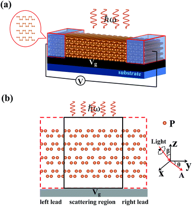
As shown in Fig. 1, the proposed nanoscale photodetector is based on two-dimensional few-layer BP. The vertical gate voltage is applied at the bottom of the entire system. In reality, the vertical gate voltage can be realized by applying a back gate voltage through a p-doped silicon wafer.28 When the vertical gate voltage is applied, the electron static potential within the few-layer BP is redistributed, which breaks its intrinsic inversion symmetry. In our numerical simulations, the model device can be divided into three parts, i.e., the central scattering region (including 6 unit cells about 27.48 Å along the armchair direction and about 18.15 Å along the zigzag direction) where light is shining, and the left and right electrodes, which extend to the electron reservoir into infinity to collect the generated photocurrent.Before presenting the quantum transport study of the proposed device, the atomic structures of few-layer BP are fully relaxed when the residual force on each atom is smaller than 0.01 eV Å−1 by using VASP.31 We perform first principles quantum transport analysis by carrying out DFT within the Keldysh non-equilibrium Green's function (NEGF) formalism,32 as implemented in the first principles quantum transport package Nanodcal.32–34 In our NEGF-DFT self-consistent calculations, a linear combination of atomic orbital basis (LCAO) at the double-ζ polarization (DZP) level is used to expand physical quantities; the standard norm-conserving nonlocal pseudo-potentials35 are used to define the atomic core. 13k points are employed for k-sampling along the transverse direction, and the energy cutoff for the real space grid is taken at 200 Ry. The NEGF-DFT self-consistency is deemed achieved when monitored quantities such as every element of the Hamiltonian and density matrices differ less than 1 × 10⁻⁵ a.u. between iteration steps. In our numerical simulations, there are two steps in order. First of all, the Hamiltonian of a two-probe device without photons is obtained self-consistently by the NEGF-DFT formalism.32 Secondly, the electron–photon interaction is perturbatively included as the self energy during the photocurrent calculations.36
In particular, we only consider the photocurrents generated by illuminating linearly or circularly polarized light on the central scattering region for the two-probe device (see Fig. 1). In the following, we shall focus on the photocurrent in the left lead of the two-probe device. Once the NEGF-DFT self-consistent device Hamiltonian is obtained, the photocurrent I(ph)L can be calculated in the following form,36,37
 | (1) |
![[thin space (1/6-em)]](https://www.rsc.org/images/entities/char_2009.gif) θe1 + sin
θe1 + sin![[thin space (1/6-em)]](https://www.rsc.org/images/entities/char_2009.gif) θe2, where θ is the angle formed by the polarized direction with respect to the vector e1 (the y axis is along the armchair direction), as shown in Fig. 1(b). In our numerical calculations, the vectors e1 and e2 are set along the y and x directions, respectively, i.e., the light is incident along the −z direction with different incidence angles β, as shown in Fig. 1(b). For the elliptically polarized light, the polarization vector is defined as e = cos
θe2, where θ is the angle formed by the polarized direction with respect to the vector e1 (the y axis is along the armchair direction), as shown in Fig. 1(b). In our numerical calculations, the vectors e1 and e2 are set along the y and x directions, respectively, i.e., the light is incident along the −z direction with different incidence angles β, as shown in Fig. 1(b). For the elliptically polarized light, the polarization vector is defined as e = cos![[thin space (1/6-em)]](https://www.rsc.org/images/entities/char_2009.gif) ϕe1 + i
ϕe1 + i![[thin space (1/6-em)]](https://www.rsc.org/images/entities/char_2009.gif) sin
sin![[thin space (1/6-em)]](https://www.rsc.org/images/entities/char_2009.gif) ϕe2. In particular, the left/right circularly polarized light can be represented when ϕ = ±45°, respectively. For simplicity, we define the normalized photocurrent to represent the photocurrent response function,37,38i.e.,
ϕe2. In particular, the left/right circularly polarized light can be represented when ϕ = ±45°, respectively. For simplicity, we define the normalized photocurrent to represent the photocurrent response function,37,38i.e., | (2) |
3 Results and discussion
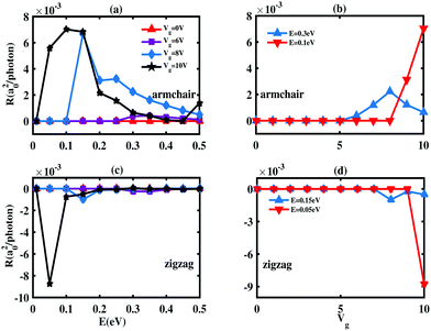
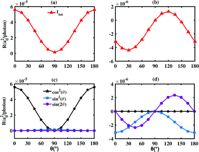
To begin with, we calculate and analyze the linearly polarized PGE (LPGE) generated photocurrent of the three-layer BP based devices (for both zigzag and armchair directions). Here, the linearly polarized light is vertically irradiated, which means the incident angle shown in Fig. 1 is equal to zero. The numerical results of the photoresponse are shown in Fig. 2. From Fig. 2(a and c), we can clearly see that the photoresponse is exactly zero in the whole photon energy range when the gate voltage Vg is equal to zero (red triangular curve) regardless of the zigzag and armchair directions. This is because there is no PGE induced photocurrent when the inversion symmetry is retained and there is no external bias and electric field to drive the photoexcited electron flow. This is consistent with the phenomenological theory.39,40 Once the gate voltage Vg is switched on, the inversion symmetry of the electron static potential of the system is broken although the atomic structure is still inversion symmetric.5 From Fig. 2(b and d), we clearly see that the nonzero photoresponse can be obtained and enlarged by increasing the gate voltage when the photon energy is fixed. More importantly, the range of the nonzero photocurrent can be gradually enlarged as the gate voltage increases. For example, as Vg is increased from 6 V to 8 V, the starting photon energy that generates nonzero photocurrent is changed from 0.25 eV into 0.1 eV, which means the photodetection range is broadened. As the inversion symmetry of the electron static potential is broken, the photogalvanic effect (PGE) is produced and hence the nonzero photocurrent can be obtained. Due to the Stark effect of few-layer BP in the presence of a vertical gate voltage, the corresponding bandgap of few-layer BP decreases. Thus, the corresponding requirement of photon energy to excite electrons between the valence band and conduction band is also reduced. Once the excitation between the valence band and conduction band occurs, the PGE induced nonzero photocurrent can be generated. This means that the starting photon energy that generates nonzero photocurrent decreases as the gate voltage increases. In fact, the photodetection range can be continuously adjusted, since the bandgap of few-layer BP can be continuously reduced through varying the applied voltage. Therefore, the middle infrared region (MIR) and the near infrared region (NIR) can both be covered. By further increasing the gate voltage Vg up to 10 V, the starting photon energy of nonzero photocurrent can be as small as 0.01 eV (∼124.03 μm) shown in Fig. 2(a and c), which is in the far infrared region (FIR). This indicates that the photodetection range can be extended to the FIR region from MIR by using the gate voltage. Furthermore, by comparing Fig. 2(a), (b) and (c), (d), the photoresponse along the armchair direction is different from that of the zigzag direction, which also reflects the giant optical anisotropy of few-layer BP. Note that the photoresponse induced by the circularly polarized current (CPGE) is similar to that of LPGE and presented in the ESI.† The anisotropic photoresponse of few-layer BP can be identified by using electrical methods.41In the following, we consider the effects of the polarization angle θ of LPGE by fixing the photon energy E = 0.025 eV. The LPGE photoresponse can be largely tuned by the polarization angle θ as shown in Fig. 3. Specifically, the photoresponse along the zigzag direction can change from negative to positive values when the polarization angle θ varies from 0° to 180°. This indicates that the polarization characteristics of light can also be detected using a few-layer BP based photodetection device. To characterize the polarization sensitivity, the extinction ratio R‖/R⊥ (R‖/⊥ is the corresponding photoresponse at polarization angles of 0° and 90°, respectively) can be introduced. The extinction ratios can reach 43.4 and 3711.2 for the photoresponse along armchair and zigzag directions. More interestingly, the photoresponse versus the polarization angle θ for both zigzag and armchair directions is quite different. This difference can be further investigated by decomposing the photoresponse into three independent terms, with factors of cos2![[thin space (1/6-em)]](https://www.rsc.org/images/entities/char_2009.gif) θ, sin2
θ, sin2![[thin space (1/6-em)]](https://www.rsc.org/images/entities/char_2009.gif) θ, and sin
θ, and sin![[thin space (1/6-em)]](https://www.rsc.org/images/entities/char_2009.gif) 2θ.42Fig. 3(c and d) presents the three components of the photoresponse in the armchair and zigzag directions, respectively. In the armchair direction case, the amplitude of the cos2
2θ.42Fig. 3(c and d) presents the three components of the photoresponse in the armchair and zigzag directions, respectively. In the armchair direction case, the amplitude of the cos2![[thin space (1/6-em)]](https://www.rsc.org/images/entities/char_2009.gif) θ term dominates and the other two terms are negligible. However, the cos2
θ term dominates and the other two terms are negligible. However, the cos2![[thin space (1/6-em)]](https://www.rsc.org/images/entities/char_2009.gif) θ term is nearly zero while sin2
θ term is nearly zero while sin2![[thin space (1/6-em)]](https://www.rsc.org/images/entities/char_2009.gif) θ and sin
θ and sin![[thin space (1/6-em)]](https://www.rsc.org/images/entities/char_2009.gif) 2θ present the most contributions. Since the photocurrent dependence on the polarization angle θ is the linear combination of three terms, the peak of photoresponse versus θ is determined by their magnitude coefficients. According to our study, the peak position can be easily tuned by changing the incident angle β. Furthermore, we can roughly estimate the photocurrent generated by the non-polarized light by taking average photocurrent over polarization angles θ, since the non-polarized light vibrates in a variety of directions and has random polarization angles. Thus, the photocurrent generated by the non-polarized light along the zigzag and armchair directions is also nonzero due to the nonzero coefficients of cos2
2θ present the most contributions. Since the photocurrent dependence on the polarization angle θ is the linear combination of three terms, the peak of photoresponse versus θ is determined by their magnitude coefficients. According to our study, the peak position can be easily tuned by changing the incident angle β. Furthermore, we can roughly estimate the photocurrent generated by the non-polarized light by taking average photocurrent over polarization angles θ, since the non-polarized light vibrates in a variety of directions and has random polarization angles. Thus, the photocurrent generated by the non-polarized light along the zigzag and armchair directions is also nonzero due to the nonzero coefficients of cos2![[thin space (1/6-em)]](https://www.rsc.org/images/entities/char_2009.gif) θ and sin2
θ and sin2![[thin space (1/6-em)]](https://www.rsc.org/images/entities/char_2009.gif) θ components. In the ESI,† the extinction ratios versus photon energies and photoresponse versus polarization angle with CPGE are presented.
θ components. In the ESI,† the extinction ratios versus photon energies and photoresponse versus polarization angle with CPGE are presented.
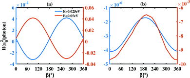
Next, we study the photoresponse versus the photon incident angle β defined in Fig. 4. Here, the polarization angle θ in LPGE is fixed as θ = 15° with two different photon energies E = 0.025, 0.05 eV (∼49.6 μm and 24.8 μm in FIR). The numerical results are presented in Fig. 4. At first glance, the photoresponses of the three-layer BP device are very sensitive with incident angle β and in all cases. As shown in Fig. 4(a), the photoresponse of LPGE along the armchair direction first decreases/increases with the increase of the incident angle β from zero when the photon energy is 0.025 eV or 0.05 eV, respectively. Furthermore, the photoresponse behavior along the zigzag direction [in Fig. 4(b)] is largely distinct. Interestingly, the photoresponse of LPGE has a periodic dependence on the incident angle β for both photon energies. In a nutshell, the photoresponse of three-layer BP is not only sensitive with photon energy and polarization angles but also sensitive with the incident angles.
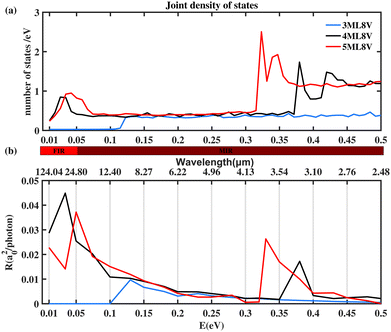
Last but not the least, the photoresponse of few-layer BP photodetection device with different layers (from three layers to five layers) is investigated by fixing the gate voltage. Since the joint density of states (JDOS)43–45 can provide optical transition information between the valence occupied bands and conduction unoccupied bands, the JDOS of few-layer BP photodetection device are studied and presented in Fig. 5(a). Firstly, we can clearly know that the JDOS of the few-layer BP photodetective devices with different layers is largely different. It is worth mentioning that the JDOS of three-layer BP is zero when the photon energy is smaller than 0.1 eV (near FIR and FIR region) and the corresponding photoresponse in this region is also zero as shown in Fig. 5(b). When the photon energy is larger than 0.1 eV, the JDOS develops into a plateau and remains a constant value. However, the corresponding photoresponse (absolute values) decreases with the increasing photon energy. More importantly, when the layer number of few-layer BP photodetection device is equal to four or five layer cases, the JDOS is nonzero in the FIR region and so is the photoresponse. In the MIR, the JDOS of four and five layer systems is further increased up to another plateau. This indicates that the layer number is also another degree of freedom to tune the photoresponse. In reality, few-layer BP should be placed on some substrate to make a real device.46 Due to the interaction between few-layer BP and the substrate material, the atomic structure of the few-layer BP shall change and the inversion symmetry of the system is broken. Then, the photoresponse of the zero gate voltage is supposed to be nonzero. Since the substrate is usually an insulating material, it has a large bandgap and an extremely small Stark effect response. Thus, the photoresponse shall only be generated by the few-layer BP and even the substrate material is also considered. However, the qualitative conclusions with non-zero gate voltage will not change. Moreover, the optoelectronic switching behavior is quite important for the practical application of the few-layer BP based photodetector.47
4 Conclusion
To summarize, using atomistic first-principles calculations, we have shown that the gate tunable few-layer BP device can be used as a broadband photodetector. Due to the presence of gate voltage, the inversion symmetry of electrostatic potential in the system is broken and hence the photocurrent can be generated and detected without an external driving force. Hence, the dark current can be greatly suppressed. More importantly, the photodetection range can be enlarged from MIR to FIR via tuning the gate voltage. Our numerical findings indicate that few-layer BP can be the potential candidate for self-powered broadband photodetectors.Conflicts of interest
There are no conflicts to declare.Acknowledgements
We gratefully acknowledge the support from the National Natural Science Foundation of China (Grants No. 11674204, 11704232, 11974355, 12074230, and 11574318), National Key R&D Program of China under Grants No. 2017YFA0304203 and 1331KSC, Shanxi Province 100-Plan Talent Program, and the Program of State Key Laboratory of Quantum Optics and Quantum Optics Devices (No. KF201810). This research was partially conducted using the High Performance Computer of Shanxi University.References
- L. Li, Y. Yu, G. J. Ye, Q. Ge, X. Ou, H. Wu, D. Feng, X. H. Chen and Y. Zhang, Nat. Nanotechnol., 2014, 9, 372–377 CrossRef CAS.
- J. Qiao, X. Kong, Z. Hu, F. Yang and W. Ji, Nat. Commun., 2014, 5, 4475 CrossRef CAS.
- H. Doh and H. J. Choi, 2D Mater., 2017, 4, 025017 CrossRef.
- H. F. Lin, L. M. Liu and J. Zhao, J. Mater. Chem. C, 2017, 5, 2291–2300 RSC.
- S. Li, T. Wang, X. Chen, W. Lu, Y. Xie and Y. Hu, Nanoscale, 2018, 10, 7694–7701 RSC.
- A. Hua, J. Zhao and N. Wei, Appl. Phys. Lett., 2019, 115, 243103 CrossRef.
- L. M. Kern, R. Galceran, V. Zatko, M. Galbiati, F. Godel, D. Perconte, F. Bouamrane, E. Gaufres, A. Loiseau, P. Brus, O. Bezencenet, M. B. Martin, B. Servet, F. Petroff, B. Dlubak and P. Seneor, Appl. Phys. Lett., 2019, 114(5), 053107 CrossRef.
- R. J. Suess, J. D. Hart, E. Leong, M. Mittendorff and T. E. Murphy, APL Photonics, 2019, 4, 034502 CrossRef.
- L. Huang and J. Li, Appl. Phys. Lett., 2016, 108, 083101 CrossRef.
- S. Jeon, J. Jia, J. H. Ju and S. Lee, Appl. Phys. Lett., 2019, 115, 183102 CrossRef.
- P. Sengupta and S. Rakheja, Appl. Phys. Lett., 2017, 111, 161902 CrossRef.
- H. Y. Wu, Y. Yen and C. H. Liu, Appl. Phys. Lett., 2016, 109, 261902 CrossRef.
- N. Youngblood and M. Li, Appl. Phys. Lett., 2017, 110, 051102 CrossRef.
- K. Gong, L. Zhang, W. Ji and H. Guo, Phys. Rev. B: Condens. Matter Mater. Phys., 2014, 90, 125441 CrossRef.
- L. Zhang, Z. Yu, L. Zhang, X. Zheng, L. Xiao, S. Jia and J. Wang, J. Mater. Chem. C, 2018, 6, 2460 RSC.
- Y. Xie, M. Chen, Z. Wu, Y. Hu, Y. Wang, J. Wang and H. Guo, Phys. Rev. Appl., 2018, 10, 034005 CrossRef CAS.
- X. Zong, H. Hu, G. Ouyang, J. Wang, R. Shi, L. Zhang, Q. Zeng, C. Zhu, S. Chen, C. Cheng, B. Wang, H. Zhang, Z. Liu, W. Huang, T. Wang, L. Wang and X. Chen, Light: Sci. Appl., 2020, 9, 114 CrossRef CAS.
- M. Buscema, D. J. Groenendijk, S. I. Blanter, G. A. Steele, H. S. van der Zant and A. Castellanos-Gomez, Nano Lett., 2014, 14(6), 3347 CrossRef CAS.
- X. Chen, X. Lu, B. Deng, O. Sinai, Y. Shao, C. Li, S. Yuan, V. Tran, K. Watanabe, T. Taniguchi, D. Naveh, L. Yang and F. Xia, Nat. Commun., 2017, 8, 1672 CrossRef.
- Y. Deng, Z. Luo, N. J. Conrad, H. Liu, Y. Gong, S. Najmaei, P. M. Ajayan, J. Lou, X. Xu and P. D. Ye, ACS Nano, 2014, 8(8), 8292–8299 CrossRef CAS.
- Q. Guo, A. Pospischil, M. Bhuiyan, H. Jiang, H. Tian, D. Farmer, B. Deng, C. Li, S. J. Han, H. Wang, Q. Xia, T. P. Ma, T. Mueller and F. Xia, Nano Lett., 2016, 16(7), 4648–4655 CrossRef CAS.
- M. Huang, M. Wang, C. Chen, Z. Ma, X. Li, J. Han and Y. Wu, Adv. Mater., 2016, 28, 3481–3485 CrossRef CAS.
- N. Youngblood, C. Chen, S. J. Koester and M. Li, Nat. Photonics, 2015, 9(4), 247–252 CrossRef CAS.
- M. Long, A. Gao, P. Wang, H. Xia, C. Ott, C. Pan, Y. Fu, E. Liu, X. Chen, W. Lu, T. Nilges, J. Xu, X. Wang, W. Hu and F. Miao, Sci. Adv., 2017, 3(6), e1700589 CrossRef.
- J. Miao, B. Song, Q. Li, L. Cai, S. Zhang, W. Hu, L. Dong and C. Wang, ACS Nano, 2017, 11(6), 6048–6056 CrossRef CAS.
- L. Su, W. Yang, J. Cai, H. Chen and X. Fang, Small, 2017, 13, 1701687 CrossRef.
- Q. Liu, X. Zhang, L. Abdalla, A. Fazzio and A. Zunger, Nano Lett., 2015, 15(2), 1222–1228 CrossRef CAS.
- Y. Liu, Z. Qiu, A. Carvalho, Y. Bao, H. Xu, S. J. R. Tan, W. Liu, A. H. Castro Neto, K. P. Loh and J. Lu, Nano Lett., 2017, 17, 1970–1977 CrossRef CAS.
- J. Kim, S. S. Baik, S. H. Ryu, Y. Sohn, S. Park, B. G. Park, J. Denlinger, Y. Yi, H. J. Choi and K. S. Kim, Science, 2015, 349, 723–726 CrossRef CAS.
- D. Li, J. R. Xu, K. Ba, N. Xuan, M. Chen, Z. Sun, Y. Z. Zhang and Z. Zhang, 2D Mater., 2017, 4, 031009 CrossRef.
- G. Kresse and J. Furthmĺźller, Phys. Rev. B: Condens. Matter Mater. Phys., 1996, 54, 11169 CrossRef CAS.
- J. Taylor, H. Guo and J. Wang, Phys. Rev. B: Condens. Matter Mater. Phys., 2001, 63, 245407 CrossRef.
- D. Waldron, P. Haney, B. Larade, A. MacDonald and H. Guo, Phys. Rev. Lett., 2006, 96, 166804 CrossRef.
- For details of the NanoDcal quantum tranpsort package, see http://hzwtech.com/.
- L. Kleinman and D. M. Bylander, Phys. Rev. Lett., 1982, 48, 1425 CrossRef CAS.
- L. Zhang, K. Gong, J. Chen, L. Liu, Y. Zhu, D. Xiao and H. Guo, Phys. Rev. B: Condens. Matter Mater. Phys., 2014, 90, 195428 CrossRef.
- J. Chen, Y. Hu and H. Guo, Phys. Rev. B: Condens. Matter Mater. Phys., 2012, 85, 155441 CrossRef.
- L. E. Henrickson, J. Appl. Phys., 2002, 91, 6273–6281 CrossRef CAS.
- E. L. Ivchenko and G. E. Pikus, JETP Lett., 1978, 27, 604 Search PubMed.
- V. I. Belinicher and B. I. Sturman, Sov. Phys. Usp., 1980, 23, 199–223 CrossRef.
- M. A. Hernández-Acosta, M. Trejo-Valdez, J. H. Castro-Chacón, C. R. Torres-San Miguel, H. Martínez-Gutiérrez and C. Torres-Torres, New J. Phys., 2018, 20, 023048 CrossRef.
- Y. Xie, L. Zhang, Y. Zhu, L. Liu and H. Guo, Nanotechnology, 2015, 26, 455202 CrossRef.
- S. K. O'Leary, J. Appl. Phys., 2004, 96(7), 3680–3686 CrossRef.
- J. J. Thevaril and S. K. O'Leary, J. Appl. Phys., 2010, 107(8), 083105 CrossRef.
- W. M. Luo, Z. G. Shao, X. F. Qin and M. Yang, Phys. E, 2020, 115, 113714 CrossRef CAS.
- E. Jiménez-Marín, I. Villalpando, M. Trejo-Valdez, F. Cervantes-Sodi, J. R. Vargas-García and C. Torres-Torres, Mater. Sci. Eng., B, 2017, 220, 22–29 CrossRef.
- C. Torres-Torres, D. Torres-Torres, M. A. García-Zíćrate, C. I. García-Gil, C. C. Leyva-Porras, O. O. Solís-Canto, M. Trejo-Valdez, A. V. Khomenko and G. Romero-Paredes, J. Mod. Opt., 2014, 61, 1500 CrossRef CAS.
Footnote |
| † Electronic supplementary information (ESI) available. See DOI: 10.1039/d0cp05292b |
| This journal is © the Owner Societies 2021 |

