
9.7%-efficient Sb2(S,Se)3 solar cells with a dithieno[3,2-b: 2′,3′-d]pyrrole-cored hole transporting material†
Chenhui
Jiang‡
 a,
Jie
Zhou‡
b,
Rongfeng
Tang
a,
Weitao
Lian
a,
Xiaomin
Wang
a,
Xunyong
Lei
c,
Hualing
Zeng
c,
Changfei
Zhu
a,
Weihua
Tang
*b and
Tao
Chen
*a
a,
Jie
Zhou‡
b,
Rongfeng
Tang
a,
Weitao
Lian
a,
Xiaomin
Wang
a,
Xunyong
Lei
c,
Hualing
Zeng
c,
Changfei
Zhu
a,
Weihua
Tang
*b and
Tao
Chen
*a
aHefei National Laboratory for Physical Sciences at Microscale, CAS Key Laboratory of Materials for Energy Conversion, Department of Materials Science and Engineering, School of Chemistry and Materials Science, University of Science and Technology of China, Hefei, 230026, China. E-mail: tchenmse@ustc.edu.cn
bSchool of Chemical Engineering, Nanjing University of Science and Technology, Nanjing 210094, China. E-mail: whtang@njust.edu.cn
cICQD, Hefei National Laboratory for Physical Sciences at Microscale, CAS Key Laboratory of Strongly-coupled Quantum Matter Physics, University of Science and Technology of China, Hefei 230026, China
First published on 8th December 2020
Abstract
Antimony selenosulfide, Sb2(S,Se)3, is a promising next-generation solar cell material with superior photovoltaic properties and high stability. However, the efficiency of Sb2(S,Se)3 solar cells lags far behind its theoretical value and other well-established thin-film solar cells. Herein, we report a one-step hydrothermal process by employing selenourea as a selenium source for a single-phase and compact Sb2(S,Se)3 light absorber film, which possessed a desirable bandgap of 1.50 eV. When a low-cost and planar dithieno[3,2-b:2′,3′-d]pyrrole-cored small molecule (DTPThMe-ThTPA) is used as the hole transporting material, the interfacial energy level alignment is optimized. We disclose that chemical interaction formed between neighbouring thiophene and Sb atoms is critical for carrier collection and suppression of charge recombination, resulting in a champion efficiency of 9.7% with DTPThMe-ThTPA and increased stability, which is comparable to the device based on conventional Spiro-OMeTAD.
Broader contextDue to the suitable photovoltaic properties and high stability, antimony selenosulfide, Sb2(S,Se)3, has emerged as a promising solar cell material. The high-efficiency Sb2(S,Se)3 solar cells typically apply expensive and hygroscopic Spiro-OMeTAD as a hole-transporting material (HTM), which poses a potential challenge to the practical applications. Here, we developed a low-cost and highly stable alternative organic HTM (denoted as DTPThMe-ThTPA) for Sb2(S,Se)3 solar cells. It is found that the planar HTM with electron-rich thiophene moieties could coordinate with Sb atoms at the interface of Sb2(S,Se)3/DTPThMe-ThTPA, thereby forming an efficient pathway of hole transport. Benefiting from the optimized interfacial energy level alignment and diminished charge recombination, DTPThMe-ThTPA-based Sb2(S,Se)3 solar cells achieved an efficiency of 9.7% with essentially increased stability. In addition to the cost-effective characteristic, the chemical interaction formed between the thiophene units of the HTM and Sb atoms of the Sb2(S,Se)3 light absorber film provides an effective strategy towards the exploitation of efficient HTMs with the dual functions of surface passivation and device performance improvement. |
Antimony chalcogenides have emerged as promising alternative light absorber materials due to their superior optoelectronic properties such as strong absorption coefficient (>105 cm−1) and easily tunable bandgap in range of 1.1–1.8 eV.1–3 In terms of practical applications, they are relatively non-toxic, less expensive, earth abundant, and stable against moisture and air.4–6 The critical challenge in this emerging solar cell technology is to improve the power conversion efficiency (PCE). To prepare efficient antimony chalcogenide solar cells, different device structures were explored. For example, the superstrate structures were initially applied to fabricate a series of antimony chalcogenide solar cells, delivering the PCEs of 7.5% and 7.6% for Sb2S3 and Sb2Se3 solar cells, respectively.7,8 Subsequently, the substrate configuration based on the Mo-coated glass substrate was introduced to prepare Sb2Se3 solar cells, recently obtaining the highest efficiency of 9.2%.9 However, this efficiency is much inferior to state-of-the-art cadmium telluride (CdTe), copper indium gallium selenide (Cu(In,Ga)Se2) and other kinds of thin-film solar cell (e.g., dye-sensitized solar cells and perovskite solar cells) as well as its maximum theoretical value.10–14
To improve the device performance, in addition to the fabrication of high quality absorber materials, interfacial materials are crucial for the fast carrier transfer from light absorber materials to the charge transfer layers. In this regard, interfacial engineering of the Sb-based absorber layers with inorganic and organic hole transporting materials (HTMs), such as CuSCN, PbS, V2O5, 2,2′,7,7′-tetrakis(N,N-di-p-methoxyphenylamino)-9,9′-spirobifluorene (Spiro-OMeTAD), poly(3-hexylthiophene) (P3HT), poly(2,6-(4,4-bis-(2-ethylhexyl)-4H-ctckioebta[2,1-b; 3,4-b′]dithiophene)-alt-4,7(2,1,3-benzothiadiazole)) (PCPDTBT), and passivation treatments were developed to boost the carrier collection efficiency and reduce carrier recombination loss at the back contact.15–19 At present, Spiro-OMeTAD has been confirmed as the most efficient HTM to deliver the highest PCE. However, Spiro-OMeTAD shows relatively low hole mobility, low conductivity, and high cost due to the complicated multistep synthesis. The lack of strong chemical interaction between Spiro-OMeTAD and antimony chalcogenide poses a potential challenge in essentially promoting the charge transfer efficiency. Therefore, alternative organic HTMs with suitable energy levels, high hole mobility and interfacial interaction are intensively demanded for improving the performance of antimony chalcogenide solar cells.
Very recently, a hydrothermal process was demonstrated as a successful approach to fabricate efficient Sb2(S,Se)3 solar cells. Treating a hydrothermally-synthesized Sb2S3 thin film with post-selenization, a highly crystalline and compact Sb2(S,Se)3 film with a device efficiency of 6.14% was realized.20 Limited by post-selenization, nonetheless, only superficial Sb2S3 is transformed into Sb2(S,Se)3. The obtained 1.63 eV bandgap of this Sb2(S,Se)3 film is larger than the optimum value. In this work, we report the direct fabrication of a single-phase and dense Sb2(S,Se)3 film via a one-step hydrothermal method with a suitable bandgap. Meanwhile, we introduce a thiophene-rich dithieno[3,2-b:2′,3′-d]pyrrole-cored organic small molecule (denoted as DTPThMe-ThTPA) as the HTM. Compared to Spiro-OMeTAD, this HTM demonstrates a higher doped hole mobility, deeper-lying highest occupied molecular orbital (HOMO) level and comparable thermal stability. The Sb2(S,Se)3/DTPThMe-ThTPA heterojunction forms bidentate-chelating between thiophene and Sb on the interfaces, which is highly desirable for enabling high hole extraction efficiency.
Fig. 1a reveals a highly crystalline characteristic for the as-prepared Sb2(S,Se)3 film (detailed synthesis is provided in the ESI†), the diffraction pattern shows a typical stibnite structure. Compared with the standard pattern of Sb2S3 (PDF 00-042-1393), the X-ray diffraction peaks of Sb2(S,Se)3 shift to lower 2-theta angles, indicating the enlarged lattice spacing that resulted from the partial substitution of S atoms by larger Se atoms. Furthermore, no diffraction peaks belonging to Sb2S3, Sb2Se3 and other impurities are observed in our samples, suggesting the formation of a single-phase Sb2(S,Se)3 film. The scanning electron microscopy (SEM) image demonstrates a uniform and compact surface morphology with the grain size up to 2 μm for the Sb2(S,Se)3 film (Fig. 1b). We further used energy dispersive X-ray spectroscopy (EDS) measurement to identify the atomic ratio of Sb, S and Se. As displayed in Fig. 1c, sharp energy peaks of Sb, S and Se are observed with an atomic ratio of 1![[thin space (1/6-em)]](https://www.rsc.org/images/entities/char_2009.gif) :1.21:0.25. Elemental mapping images confirm the uniform distribution of Sb, S and Se through the Sb2(S,Se)3 film (Fig. S7, ESI†).
:1.21:0.25. Elemental mapping images confirm the uniform distribution of Sb, S and Se through the Sb2(S,Se)3 film (Fig. S7, ESI†).
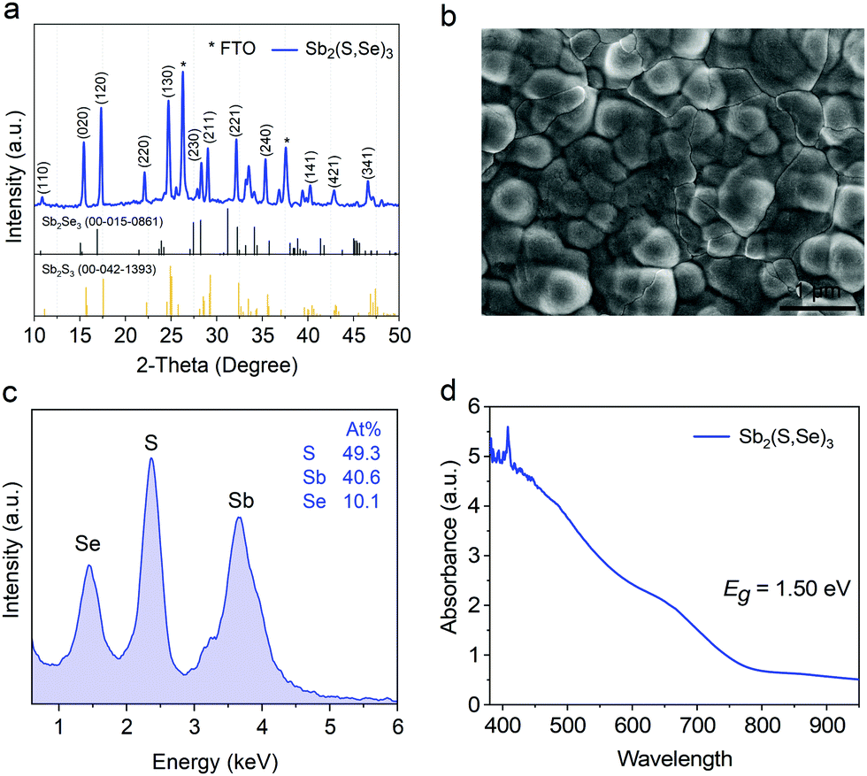 | ||
| Fig. 1 (a) XRD pattern, (b) SEM image (top-view), (c) EDS spectrum, and (d) UV-vis absorption spectrum of the as-synthesized Sb2(S,Se)3 film. | ||
The ultraviolet-visible (UV-vis) absorption spectrum shows that the as-prepared Sb2(S,Se)3 film can efficiently harvest the sunlight in the entire visible region with an absorption onset of 825 nm (Fig. 1d). The optical bandgap of the Sb2(S,Se)3 film is determined to be 1.50 eV, approaching the theoretical optimal value (Fig. S8a, ESI†). Synchrotron radiation photoemission spectroscopy (SRPES) results demonstrate a valence band maximum (VBM) and conduction band minimum (CBM) of −5.37 eV and −3.87 eV for our Sb2(S,Se)3 film, respectively (Fig. S8b–d, ESI†). These results suggest that the Sb2(S,Se)3 film fabricated via a one-step hydrothermal procedure without further post-selenization is suitable as a light absorber for photovoltaic devices. In terms of complete devices, Sb2(S,Se)3 solar cells fabricated via a hydrothermal deposition method without HTMs deliver poor PCE with extremely low open-circuit voltage (Voc) and fill factor (FF) owing to the low built-in potential.21 Moreover, it should be noted that the nonmetal elements in the as-prepared Sb2(S,Se)3 film are deficient, as the EDS results show in Fig. 1c. Previous theoretical and experimental results22,23 demonstrated the easy formation of cation-replaced-anion antisites and anion vacancies under Sb-rich conditions because of their low formation energies. These deep-level donor defects can result in increased unpaired Sb atoms, which could serve as charge recombination centers specifically on the surface and grain boundaries. To address this problem, a conjugated planar small molecule is employed as an alternative HTM to improve carrier extraction efficiency and reduce the recombination rate.
DTPThMe-ThTPA was synthesized according to our previous protocol (Scheme S1, ESI†).24 The detailed synthetic procedure and characterization of chemical structures are presented in the ESI,† (Fig. S1–S6). The cost for lab synthesis of DTPThMe-ThTPA is estimated to be approximately 20 $ g−1 (Table S1, ESI†), which is much lower than that of Spiro-OMeTAD (250 $ g−1). The characteristics of DTPThMe-ThTPA and Spiro-OMeTAD are summarized in Table S2 (ESI†). In particular, as revealed by density functional theory (DFT) calculation (Fig. S9, ESI†), DTPThMe-ThTPA displays a planar conjugated structure, which significantly differs from orthogonal Spiro-OMeTAD. A significant redshift (ca. 91 nm) of the maximum absorption band was thus observed for DTPThMe-ThTPA (Fig. S10a, ESI†).25,26 The optical bandgaps of DTPThMe-ThTPA and Spiro-OMeTAD are derived to be 2.21 and 2.95 eV, respectively (Fig. S10b, ESI†). Based on the onset of the first oxidation peak in cyclic voltammetry (CV) curves (Fig. S11, ESI†), the highest occupied molecular orbital (HOMO) energy levels of DTPThMe-ThTPA and Spiro-OMeTAD are determined to be −4.87 eV and −4.82 eV, respectively. Both the HOMO values are shallower than the VBM of Sb2(S,Se)3 film, guaranteeing hole extraction from the light absorber. Meanwhile, the lowest unoccupied molecular orbital (LUMO) energy levels of DTPThMe-ThTPA and Spiro-OMeTAD are calculated to be −2.66 and −1.87 eV, respectively, which are able to block electrons. These CV results are well consistent with the DFT calculation (Fig. 2a). The space-charge-limited current (SCLC) method was conducted to evaluate the hole-transporting properties of DTPThMe-ThTPA and Spiro-OMeTAD. As shown in Fig. S12 (ESI†), the hole mobility of the DTPThMe-ThTPA film in low doped concentration is estimated to be 1.67 × 10⁻³ cm2 V−1 s−1, which is higher than doped Spiro-OMeTAD (8.02 × 10⁻⁴ cm2 V−1 s−1). We attribute the improved hole mobility to the enhanced π–π molecular stacking and intramolecular charge transfer. The deeper HOMO level and higher hole mobility of DTPThMe-ThTPA make the hole extraction and transport more favorable.
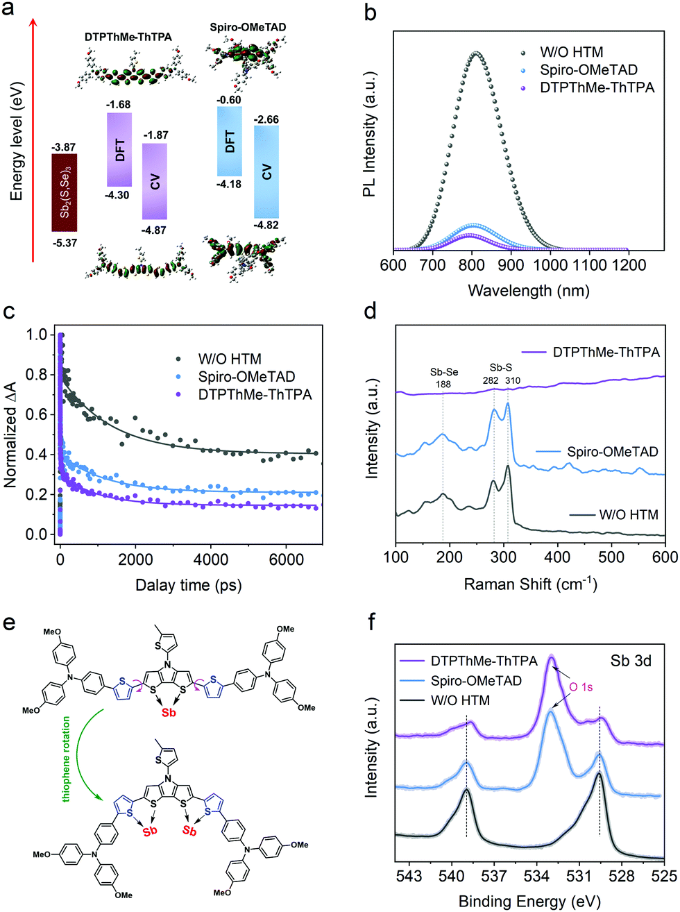 | ||
| Fig. 2 (a) Energy-level diagram of Sb2(S,Se)3, DTPThMe-ThTPA and Spiro-OMeTAD. (b) Steady-state PL spectra, (c) TAS decay kinetics at 650 nm, (d) Raman spectra, and (f) Sb 3d XPS spectra of FTO/CdS/Sb2(S,Se)3, FTO/CdS/Sb2(S,Se)3/DTPThMe-ThTPA and FTO/CdS/Sb2(S,Se)3/Spiro-OMeTAD films. (e) Schematic illustration of the chelating effect for neighboring thiophene moieties toward Sb atoms. | ||
The interfacial hole transporting properties were further investigated by steady-state photoluminescence (PL) spectra (Fig. 2b). The PL intensities of the Sb2(S,Se)3 films are found to be quenched more effectively by attaching DTPPhMe-ThTPA, which is in good agreement with the above analyses. Furthermore, the PL peak of Sb2(S,Se)3/DTPThMe-ThTPA shows an obvious blueshift due to a lower trap state density on the light absorber surface.27,28 We consider that electron-rich thiophene groups could act as Lewis bases to coordinate with Sb atoms, especially un-coordinated Sb atoms at the interface of Sb2(S,Se)3/DTPThMe-ThTPA, thereby forming an efficient pathway of hole transfer. Transient absorption spectroscopy (TAS) was employed to gain insight into the carrier dynamics. The transition dynamics were extracted from pseudo-color TAS (Fig. S13, ESI†) and can be well fitted with the monoexponential equation. As shown in Fig. 2c, FTO/CdS/Sb2(S,Se)3 has a long carrier lifetime of 1384 ps, which is consistent with the literature.8,29 Capped with HTMs, the DTPThMe-ThTPA sample (827 ps) exhibits a faster delay lifetime than Spiro-OMeTAD (973 ps), suggesting a better hole extraction ability.
Raman spectra (Fig. 2d) clearly demonstrate the characteristic Sb–S bond vibration (282 and 310 cm−1) and Sb–Se bond vibration (188 cm−1) for Sb2(S,Se)3.30 The attachment of doped or undoped Spiro-OMeTAD has a negligible effect on the Sb-chalcogen bonds (Fig. S14, ESI†). However, the use of DTPThMe-ThTPA leads to the disappearance of these chemical bonds, suggesting the presence of interfacial interactions. In the case of DTPThMe-ThTPA, two types of neighboring thiophene exist which result from the dithieno[3,2-b:2′,3′-d]pyrrole core and rotatable thiophene bridges (Fig. 2e). As such, DTPThMe-ThTPA is able to passivate the interfaces by forming stable complexes to replace these Sb–chalcogen bonds. X-ray photoelectron spectroscopy (XPS) measurement was also performed to deeply understand the passivation effect. As depicted in Fig. 2f, with the deposition of DTPThMe-ThTPA, the Sb 3d peaks display an apparent shift to lower binding energy as compared to the pristine Sb2(S,Se)3 and Sb2(S,Se)3/Spiro-OMeTAD, indicating that the electron density around Sb atoms is increased, which could be ascribed to the interactions with electron-rich thiophene moieties.31 These results indicate the accelerated charge transport and suppressed interfacial charge recombination loss for DTPThMe-ThTPA based devices and an increased device performance is expected. Furthermore, DTPThMe-ThTPA possesses a comparable thermal stability in comparison to Spiro-OMeTAD. As depicted in Fig. S15 (ESI†), the differential scanning calorimetry thermograms show that the glass transition temperature (Tg) of DTPThMe-ThTPA (120 °C) is opportunely equivalent to Spiro-OMeTAD. In addition, the thermogravimetric analysis result reveals a high decomposition temperature with 5% weight loss (Td95) of 426 °C for DTPThMe-ThTPA.
In order to demonstrate the potential of this HTM, we fabricated devices in a configuration of FTO (fluorine doped tin oxide)/CdS/Sb2(S,Se)3/HTM/Au by using either DTPThMe-ThTPA or Spiro-OMeTAD as HTMs. First, it is imperative to optimize the film thickness of DTPThMe-ThTPA for the best PCE, where the thickness was tuned by spin-coating different concentrations of DTPThMe-ThTPA from 4 to 16 mg mL−1. As illustrated in Fig. S16 (ESI†), with the DTPThMe-ThTPA concentration increasing, the devices initially display an improvement and then a drop in PCE. The reason for this is that too thin HTM film cannot effectively block electrons due to the appearance of pinholes or incomplete coverage of Sb2(S,Se)3. This results in direct contact between the gold electrode and the Sb2(S,Se)3 film. On the other hand, too thick HTM film would increase resistance, which leads to impeded charge transport.32 The optimal DTPThMe-ThTPA thickness of ∼90 nm was achieved from a low precursor concentration of merely 8 mg mL−1, which is much lower than that of Spiro-OMeTAD (36.6 mg mL−1). Coupling with lower amount of additives, the application of DTPThMe-ThTPA as the HTM implies low material consumption and thus low cost production.
Fig. 3a shows the cross-sectional SEM image of the typical device with the optimized 90 nm thick DTPThMe-ThTPA layer uniformly attaching the surface of a 300 nm thick Sb2(S,Se)3 layer. To evaluate the advantage of DTPThMe-ThTPA, Sb2(S,Se)3 solar cells without the HTM (denoted as W/O HTM) and with the Spiro-OMeTAD layer (denoted as Spiro-OMeTAD) were fabricated as reference devices. The current density–voltage (J–V) curves of the best performing devices measured under standard simulated AM1.5G are displayed in Fig. 3b. The corresponding photovoltaic parameters are summarized in Table 1. The W/O HTM device shows a rather low PCE of 5.60%, which can be ascribed to low Voc, short-circuit current density (Jsc), and FF. From the statistics of a series of devices (Table 1 and Fig. S17, ESI†), the average Voc, FF and Jsc of the Spiro-OMeTAD based devices are 619 mV, 22.94 mA cm−2 and 62.27%, while the DTPThMe-ThTPA devices exhibit average Voc, FF and Jsc of 634 mV, 22.69 mA cm−2 and 64.52%, respectively. The change in average efficiencies is consistent with the best efficiencies of the devices based on the two HTMs. The best DTPThMe-ThTPA device achieves a PCE of 9.69%. Fig. 3c depicts the measured external quantum efficiency (EQE) spectrum of the champion device using DTPThMe-ThTPA as the HTM. In the visible region of 530–580 nm, the peak EQE can reach up to 90% with an integrated Jsc of 22.00 mA cm−2, which is close to the Jsc obtained from the J–V measurements. It is worth noting that the EQE is low in the short wavelength region, where considerable photons are absorbed by the CdS buffer layer because of its bandgap of ∼2.4 eV.33,34 In order to demonstrate the repeatability, 101 independent cells were fabricated and characterized. The PCE histogram displayed in Fig. 3d demonstrates a good reproducibility for the devices with DTPThMe-ThTPA as the HTM, where most of the devices deliver PCEs above 8.7%.
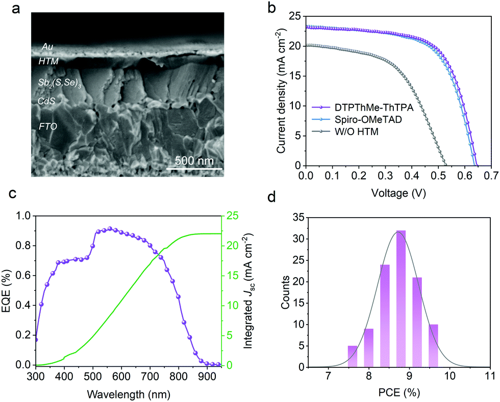 | ||
| Fig. 3 (a) Cross-sectional SEM image of the typical device with DTPThMe-ThTPA as the HTM. (b) Current density–voltage (J–V) curves of W/O HTM, Spiro-OMeTAD, and DTPThMe-ThTPA devices. (c) EQE curve of the best DTPThMe-ThTPA device (purple) and the integrated short-circuit current density (green). (d) A PCE distribution for 101 DTPTh Me-ThTPA devices. | ||
| HTMs | V oc (mV) | J sc (mA cm−2) | FF (%) | η (%) |
|---|---|---|---|---|
| W/O HTM | 486 ± 37 (529) | 19.27 ± 1.20 (20.12) | 47.14 ± 3.74 (52.69) | 4.32 ± 0.68 (5.60) |
| Spiro-OMeTAD | 619 ± 13 (630) | 22.94 ± 0.51 (23.31) | 62.27 ± 1.51 (63.85) | 8.90 ± 0.26 (9.37) |
| DTPThMe-ThTPA | 634 ± 9 (638) | 22.69 ± 0.40 (23.18) | 64.52 ± 0.97 (65.50) | 9.28 ± 0.26 (9.69) |
To investigate the interfacial charge transfer properties of the devices, we carried out electrochemical impedance spectroscopy (EIS) measurements. Fig. 4a presents the Nyquist plots of the devices. The high- and low-frequency components correspond to charge transfer resistance (Rs) and recombination resistance (Rrec), respectively. As summarized in Table S3 (ESI†), the device with DTPThMe-ThTPA exhibits a larger Rrec and smaller Rs than those of the Spiro-OMeTAD device. These results indicate that DTPThMe-ThTPA HTM enables more efficient hole transport and slower charge recombination rate. Without HTMs, the Sb2(S,Se)3 solar cells suffer from severe charge recombination along with the highest charge transfer barrier among the devices. Fig. 4b shows capacitance–voltage (C–V) characteristic curves of various devices. The built-in potential of the DTPThMe-ThTPA device (0.665 V) is found to be higher than the Spiro-OMeTAD device (0.653 V), which thus results in an improvement of Voc.35
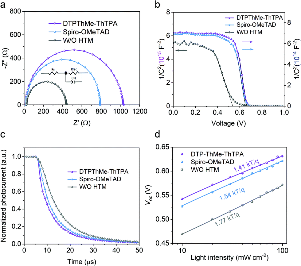 | ||
| Fig. 4 (a) Nyquist plots, (b) Mott–Schottky plots, (c) transient photocurrent delay curves and (d) the dependence of Voc on different light intensity for the W/O HTM, Spiro-OMeTAD, and DTPThMe-ThTPA devices. The insert image in (a) is the corresponding equivalent circuit. | ||
We also conducted transient photocurrent decay measurement to further characterize the charge transport mechanism in the devices. As shown in Fig. 4c, the DTPThMe-ThTPA device exhibits the shortest photocurrent decay time compared to W/O HTM and Spiro-OMeTAD devices, indicating an enhanced charge extraction ability for DTPThMe-ThTPA.36Fig. 4d shows a linear relationship between Voc and the logarithm of light intensity. Compared to W/O HTM (1.77 kT/q) and Spiro-OMeTAD devices (1.54 kT/q), the DTPThMe-ThTPA device exhibits the smallest slope of 1.41 kT/q, indicating a reduced trap-assisted Shockley–Read–Hall recombination,37,38 which is in agreement with the observations discussed above. To summarize, all the above results confirm that planar molecular DTPThMe-ThTPA is an effective HTM for Sb2(S,Se)3 solar cells, which not only efficiently extracts the holes but also passivates the defects and suppresses the charge recombination.
The stability of the as-prepared devices was investigated with devices stored in the ambient air with relative humidity (RH) >15% and room temperature without encapsulation. A general observation is that DTPThMe-ThTPA devices always display better stability than Spiro-OMeTAD based devices (Fig. 5a, b and Fig. S18, Table S4, ESI†). In particular, the DTPThMe-ThTPA device retains over 92% of the initial efficiency after storing for 30 days (Fig. 5a), whereas the PCE of the Spiro-OMeTAD device degrades relatively fast to 79% of its initial value under the same storage condition (Fig. 5b). We assume that the chemical interaction between DTPThMe-ThTPA and Sb2(S,Se)3 improved the heterojunction quality and device stability. We measured the water contact angles of both HTM films, as shown in Fig. 5c and d, and found that the contact angle on the surface of the DTPThMe-ThTPA film (86°) is larger than that of Spiro-OMeTAD (67°). The increased hydrophobicity generated by using DTPThMe-ThTPA as the HTM is a key factor contributing to the enhanced stability of Sb2(S,Se)3 devices.
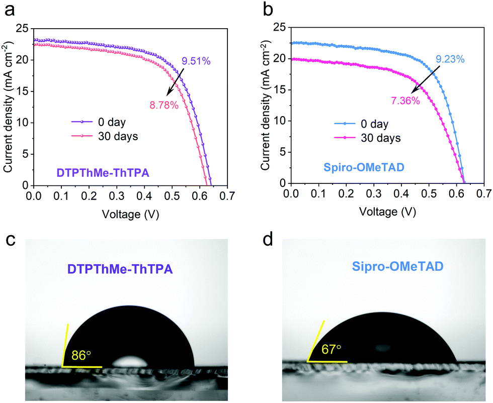 | ||
| Fig. 5 The J–V curves of (a) DTPThMe-ThTPA and (b) Spiro-OMeTAD devices measured at the beginning and after storage in ambient air for 30 days. Contact angle measurements by dropping water on the top of (c) DTPThMe-ThTPA and (d) Spiro-OMeTAD films, respectively. | ||
In summary, we have demonstrated a straightforward and feasible approach to deposit a single-phase Sb2(S,Se)3 film with compact morphology and optimal bandgap. Taking advantage of the conjugated thiophene-rich HTM, the hole transport at the Sb2(S,Se)3/HTM interface is improved with favorable energy level alignment. The application of DTPThMe-ThTPA as the HTM introduced critical interfacial functionalization which enhanced charge transport and diminished charge recombination. Benefitting from these results, the champion DTPThMe-ThTPA-based Sb2(S,Se)3 solar cells achieved a PCE value of 9.69%, suggesting a breakthrough in the performance improvement of Sb2(S,Se)3 solar cells. Furthermore, the device with DTPThMe-ThTPA showed essentially improved operational stability compared with the Spiro-OMeTAD-based device. This research suggests that DTPThMe-ThTPA is a promising HTM candidate for the development of high-efficiency Sb2(S,Se)3 solar cells and other types of photovoltaic cells.
Conflicts of interest
There are no conflicts to declare.Acknowledgements
This work was supported by the National Natural Science Foundation of China (U19A2092, 21905136, and 22005293), the National Key Research and Development Program of China (2019YFA0405600), the Fundamental Research Funds for the Central Universities (WK2340000082 and WK2030020032), and Collaborative Innovation Program of Hefei Science Center, CAS.Notes and references
- R. Kondrotas, C. Chen and J. Tang, Joule, 2018, 2, 857–878 CrossRef CAS.
- Y. C. Choi, T. N. Mandal, W. S. Yang, Y. H. Lee, S. H. Im, J. H. Noh and S. I. Seok, Angew. Chem., Int. Ed., 2014, 53, 1329–1333 CrossRef CAS PubMed.
- K. Li, C. Chen, S. Lu, C. Wang, S. Wang, Y. Lu and J. Tang, Adv. Mater., 2019, 31, 1903914 CrossRef CAS PubMed.
- Y. Zhou, L. Wang, S. Chen, S. Qin, X. Liu, J. Chen, D.-J. Xue, M. Luo, Y. Cao, Y. Cheng, E. H. Sargent and J. Tang, Nat. Photonics, 2015, 9, 409–415 CrossRef CAS.
- L. Wang, D.-B. Li, K. Li, C. Chen, H.-X. Deng, L. Gao, Y. Zhao, F. Jiang, L. Li, F. Huang, Y. He, H. Song, G. Niu and J. Tang, Nat. Energy, 2017, 2, 17046–17055 CrossRef CAS.
- H. Lei, J. Chen, Z. Tan and G. Fang, Sol. RRL, 2019, 3, 1900026 CrossRef.
- Y. C. Choi, D. U. Lee, J. H. Noh, E. K. Kim and S. I. Seok, Adv. Funct. Mater., 2014, 24, 3587–3592 CrossRef CAS.
- X. Wen, C. Chen, S. Lu, K. Li, R. Kondrotas, Y. Zhao, W. Chen, L. Gao, C. Wang, J. Zhang, G. Niu and J. Tang, Nat. Commun., 2018, 9, 2179 CrossRef PubMed.
- Z. Li, X. Liang, G. Li, H. Liu, H. Zhang, J. Guo, J. Chen, K. Shen, X. San, W. Yu, R. E. I. Schropp and Y. Mai, Nat. Commun., 2019, 10, 125 CrossRef PubMed.
- Y. Zhao, M. Boccard, S. Liu, J. Becker, X.-H. Zhao, C. M. Campbell, E. Suarez, M. B. Lassise, Z. Holman and Y.-H. Zhang, Nat. Energy, 2016, 1, 16067 CrossRef CAS.
- A. Chirila, P. Reinhard, F. Pianezzi, P. Bloesch, A. R. Uhl, C. Fella, L. Kranz, D. Keller, C. Gretener, H. Hagendorfer, D. Jaeger, R. Erni, S. Nishiwaki, S. Buecheler and A. N. Tiwari, Nat. Mater., 2013, 12, 1107–1111 CrossRef CAS PubMed.
- Y. Wang, T. Wu, J. Barbaud, W. Kong, D. Cui, H. Chen, X. Yang and L. Han, Science, 2019, 365, 687–691 CrossRef CAS PubMed.
- M. He, B. Li, X. Cui, B. Jiang, Y. He, Y. Chen, D. O’Neil, P. Szymanski, M. A. Ei-Sayed, J. Huang and Z. Lin, Nat. Commun., 2017, 8, 16045 CrossRef CAS PubMed.
- X. Cui, Y. Chen, M. Zhang, Y. W. Harn, J. Qi, L. Gao, Z. L. Wang, J. Huang, Y. Yang and Z. Lin, Energy Environ. Sci., 2020, 13, 1743–1752 RSC.
- K. Li, S. Wang, C. Chen, R. Kondrotas, M. Hu, S. Lu, C. Wang, W. Chen and J. Tang, J. Mater. Chem. A, 2019, 7, 9665–9672 RSC.
- C. Chen, L. Wang, L. Gao, D. Nam, D. Li, K. Li, Y. Zhao, C. Ge, H. Cheong, H. Liu, H. Song and J. Tang, ACS Energy Lett., 2017, 2, 2125–2132 CrossRef CAS.
- L. Zhang, C. Jiang, C. Wu, H. Ju, G. Jiang, W. Liu, C. Zhu and T. Chen, ACS Appl. Mater. Interfaces, 2018, 10, 27098–27105 CrossRef CAS PubMed.
- Y. C. Choi and S. I. Seok, Adv. Funct. Mater., 2015, 25, 2892–2898 CrossRef CAS.
- C. Chen, K. Li, S. Chen, L. Wang, S. Lu, Y. Liu, D. Li, H. Song and J. Tang, ACS Energy Lett., 2018, 3, 2335–2341 CrossRef CAS.
- W. Wang, X. Wang, G. Chen, L. Yao, X. Huang, T. Chen, C. Zhu, S. Chen, Z. Huang and Y. Zhang, Adv. Electron. Mater., 2019, 5, 1800683 CrossRef.
- M. Courel, T. Jiménez, A. Arce-Plaza, D. Seuret-Jiménez, J. P. Morán-Lázaro and F. J. Sánchez-Rodríguez, Sol. Energy Mater. Sol. Cells, 2019, 201, 110123 CrossRef CAS.
- X. Liu, X. Xiao, Y. Yang, D.-J. Xue, D.-B. Li, C. Chen, S. Lu, L. Gao, Y. He, M. C. Beard, G. Wang, S. Chen and J. Tang, Prog. Photovoltaics Res. Appl., 2017, 25, 861–870 CrossRef CAS.
- M. Huang, P. Xu, D. Han, J. Tang and S. Chen, ACS Appl. Mater. Interfaces, 2019, 11, 15564–15572 CrossRef CAS PubMed.
- X. Yin, J. Zhou, Z. Song, Z. Dong, Q. Bao, N. Shrestha, S. S. Bista, R. J. Ellingson, Y. Yan and W. Tang, Adv. Funct. Mater., 2019, 29, 1904300 CrossRef.
- W. Tang, J. Zhou, X. Yin, Z. Dong, A. Ali, Z. Song, N. Shrestha, S. S. Bista, Q. Bao, R. J. Ellingson and Y. Yan, Angew. Chem., Int. Ed., 2019, 58, 13717–13721 CrossRef PubMed.
- N. J. Jeon, H. Na, E. H. Jung, T.-Y. Yang, Y. G. Lee, G. Kim, H.-W. Shin, S. Il Seok, J. Lee and J. Seo, Nat. Energy, 2018, 3, 682–689 CrossRef CAS.
- Z. Liu, J. Chang, Z. Lin, L. Zhou, Z. Yang, D. Chen, C. Zhang, S. F. Liu and Y. Hao, Adv. Energy Mater., 2018, 8, 1703432 CrossRef.
- D. Wang, Y. Chang, S. Pang and G. Cui, J. Semicond., 2017, 38, 014002 CrossRef.
- C. Chen and J. Tang, ACS Energy Lett., 2020, 5, 2294–2304 CrossRef CAS.
- H. Deng, S. Yuan, X. Yang, J. Zhang, J. Khan, Y. Zhao, M. Ishaq, W. Ye, Y. B. Cheng and H. Song, Prog. Photovolt. Res. Appl., 2018, 26, 281–290 CrossRef CAS.
- D. B. Sulas, A. E. London, L. Huang, L. Xu, Z. Wu, T. N. Ng, B. M. Wong, C. W. Schlenker, J. D. Azoulay and M. Y. Sfeir, Adv. Opt. Mater., 2018, 6, 1701138 CrossRef.
- W. Ke, P. Priyanka, S. Vegiraju, C. C. Stoumpos, I. Spanopoulos, C. M. M. Soe, T. J. Marks, M. C. Chen and M. G. Kanatzidis, J. Am. Chem. Soc., 2018, 140, 388–393 CrossRef CAS PubMed.
- W. Witte, S. Spiering and D. Hariskos, Vak. Forsch. Prax., 2014, 26, 23–27 CrossRef CAS.
- J. Li, Y. Ma, G. Chen, J. Gong, X. Wang, Y. Kong, X. Ma, K. Wang, W. Li, C. Yang and X. Xiao, Sol. RRL, 2019, 3, 1800254 CrossRef.
- E. H. Jung, N. J. Jeon, E. Y. Park, C. S. Moon, T. J. Shin, T. Y. Yang, J. H. Noh and J. Seo, Nature, 2019, 567, 511–515 CrossRef CAS PubMed.
- Q. Jiang, L. Zhang, H. Wang, X. Yang, J. Meng, H. Liu, Z. Yin, J. Wu, X. Zhang and J. You, Nat. Energy, 2016, 2, 16177 CrossRef.
- J. Duan, Y. Zhao, B. He and Q. Tang, Small, 2018, 14, 1704443 CrossRef PubMed.
- X. Yin, L. Guan, J. Yu, D. Zhao, C. Wang, N. Shrestha, Y. Han, Q. An, J. Zhou, B. Zhou, Y. Yu, C. R. Grice, R. A. Awni, F. Zhang, J. Wang, R. J. Ellingson, Y. Yan and W. Tang, Nano Energy, 2017, 40, 163–169 CrossRef CAS.
Footnotes |
| † Electronic supplementary information (ESI) available. See DOI: 10.1039/d0ee02239j |
| ‡ These authors contributed equally to this work. |
| This journal is © The Royal Society of Chemistry 2021 |