 Open Access Article
Creative Commons Attribution 3.0 Unported Licence
Highly efficient, ultralow turn-on voltage red and white organic light-emitting devices based on a novel exciplex host
Jian
Song
a,
Fujun
Zhang
a,
Liping
Yang
a,
Keming
Chen
a,
Asu
Li
a,
Ren
Sheng
b,
Yu
Duan
 a and
Ping
Chen
 *ab
*ab
aState Key Laboratory on Integrated Optoelectronics, College of Electronic Science and Engineering, Jilin University, Changchun, China. E-mail: pingchen@jlu.edu.cn
bInstitute of Science and Technology for Opto-Electronic Information, Yantai University, Yantai 264005, China
First published on 8th April 2021
Abstract
The exciplex forming co-host is one of the most promising candidates for developing high-performance organic light-emitting devices (OLEDs) that can implement an internal quantum efficiency of 100%. In this work, a novel exciplex co-host system by employing N-([1,1′-biphenyl]-2-yl)-N-(9,9-dimethyl-9H-fluoren-2-yl)-9,9′-spirobi[fluoren]-4-amine (FSF4A) and 2,4,6-tris[3-(diphenylphosphinyl)phenyl]-1,3,5-triazine (PO-T2T) is applied to design simplified red and white OLEDs with low turn-on voltage and high efficiency. A high performance red phosphorescent organic light-emitting diode (PhOLED) is achieved by employing an exciplex co-host in a low guest doping level of 3%, showing the best performance with a maximum power efficiency of 38.5 lm W−1, a maximum external quantum efficiency of 17.3%, and an ultralow turn-on voltage of 1.95 V, respectively. Based on the red device, the ultra-thin FIrPic layer is inserted to achieve high performance white OLEDs, exhibiting a low turn-on voltage of 2.2 V with a maximum power efficiency of 34.1 lm W−1, and the Commission Internationale de’IEclairage (CIE) coordinate (0.33,0.33) at 1000 cd m−2. These superior properties can be attributed to reduced barriers and the effective energy transfer by employing an exciplex co-host.
1. Introduction
Phosphorescent organic light-emitting diodes (PhOLEDs) have attracted great attention due to their extensive application prospects in the field of solid-state lighting and flat-panel displays with the theoretical value of 100% exciton utilization by harvesting both singlet and triplet excitons for electroluminescence (EL).1–4 In general, to improve the device efficiency and stability, host–guest technology is a superior method for designing high performance phosphorescent devices.5,6 The host materials usually need to have appropriate highest occupied molecular orbital (HOMO) and lowest unoccupied molecular orbital (LUMO) levels to facilitate balanced charge injection and transportation capabilities, as well as high triplet energy levels (T1) to ensure effective energy transfer and confine excitons in the phosphorescent guest.7–11 However, there are still huge challenges to achieve PhOLEDs with low driving voltage and low energy consumption.12,13 In order to meet the needs of high-quality red and white OLEDs, it is essential to design an advantageous emission layer structure, which can achieve high exciton utilization for both singlet and triplet, as well as effective charge injection and transportation at low voltage.14Recently, the co-host of an exciplex formed by an acceptor and a donor, instead of traditional hole or electron type single hosts, have been regarded as a promising candidate for using as a host on phosphorescent OLEDs due to its good charge balance and exciton utilization.15–20 Furthermore, it has been demonstrated that an exciplex host with small singlet–triplet energy difference (ΔEst) can notably reduce the turn-on voltage and improve the power efficiency (PE) and external quantum efficiency (EQE) of the PhOLEDs.21–23 In general, exciplex systems are found to have a thermally activated delayed fluorescence (TADF) effect through reverse intersystem crossing (RISC), triplet excitons can be upconverted to single excitons due to intrinsically smaller ΔEst values.24,25 It is found that the exciplex co-host is more beneficial to facilitate effective Förster energy transfer, which can further improve device efficiency.26,27 Many exciplex co-host systems have been reported to demonstrate high efficiency of red and white phosphorescent OLEDs with the development of an exciplex co-host. Sheng et al. adopted an exciplex co-host to achieve red phosphorescent OLEDs with a maximum power efficiency of 35.3 lm W−1 and external quantum efficiency of 19.8%.28 Xu et al. reported a red phosphorescent OLED through an exciplex co-host system with a maximum power efficiency of 31.8 lm W−1 and turn-on voltage of 2.24 V.29 Yao et al. realized a red phosphorescent device with a maximum power efficiency of 36.9 lm W−1 and external quantum efficiency of 15.5%.30 However, despite the remarkable progress in the use of exciplex co-hosts in OLEDs, it is still a great challenge to precisely predict the likelihood of electron hole pairs inducing exciplex emission and achieving ultra-low turn-on voltage PhOLEDs.
In this work, a novel exciplex system is fabricated by employing a new hole transport material of N-([1,1′-biphenyl]-2-yl)-N-(9,9-dimethyl-9H-fluoren-2-yl)-9,9′-spirobi[fluoren]-4-amine (FSF4A) and electron transport material of 2,4,6-tris[3-(diphenylphosphinyl)phenyl]-1,3,5-triazine (PO-T2T), the yellow exciplex emission can be observed in both photoluminescence (PL) and electroluminescence (EL). Compared with common mixed-host devices, the red PhOLED based on an exciplex co-host demonstrates an ultralow turn-on voltage of 1.95 V and a maximum power efficiency of 38.5 lm W−1 with an external quantum efficiency of 17.3%. Moreover, its turn-on voltage is almost the same as the lowest turn-on voltage achieved by the red OLED based on an exciplex co-host.31 By further inserting a blue ultrathin layer, the white OLED achieves an ultralow turn-on voltage of 2.2 V and a maximum power efficiency of 34.1 lm W−1 with an external quantum efficiency of 12.4%, and the turn-on voltage is almost one of the lowest compared to previous ref. 32 and 33. Furthermore, the Commission Internationale de’IEclairage (CIE) coordinates are (0.33,0.33) at 1000 cd m−2, and the CIE coordinate variation is only (0.026,0.003) over a large luminance range, which is better among the WOLEDs of exciplex co-hosts. It is found that the high performances of PhOLEDs are mainly attributed to balanced charge transport and appropriate energy transfer channels from an exciplex co-host to the dopant. This work may provide valuable clues for the rational design of exciplex systems, as well as their application as co-host materials in PhOLEDs with high efficiency and ultralow turn-on voltage.
2. Experimental section
2.1 Materials
FSF4A was purchased from Shenzhen PURI Materials Technologies Co., Ltd Ir(MDQ)2acac and FIrPic were purchased from Luminescence Technology Corp. MoO3, TPBi, MCP, Liq, and PO-T2T were purchased from Xi’an Polymer Light Technology Corp.For the basic parameters of FSF4A: S1 is 3.0 eV, T1 is 2.6 eV, HOMO is 5.3 eV, LUMO is 2.1 eV, and the absorption peak positions are 310 nm and 340 nm.
2.2 Device fabrication and characterization
The OLED were grown on pre-patterned ITO coated glass (20 Ω per square). Before depositing into the evaporation system, the ITO substrates were cleaned with acetone, ethyl alcohol, and deionized water using an ultrasonic cleaning machine for 20 min. All the devices were deposited sequentially under a fine vacuum of 8 × 10⁻⁵ Pa. The organic transport materials were grown at a rate of 0.8–1.5 Å s−1, while organic dopants Ir(MDQ)2acac and FIrPic were deposited at a rate of 0.01–0.1 Å s−1, the FIrPic ultra-thin layer of 0.2 nm is deposited at a rate of 0.05 Å s−1 for 40 s, Liq and MoO3 were deposited at a rate of 0.15–0.3 Å s−1, and Al was deposited at a rate of 3 Å s−1.The photoluminescence (PL) spectra were acquired by an RF-5301PC fluorescence spectrophotometer. The transient PL decay curves were recorded using an IHR320 spectrometer. The CIE coordinates, luminance and electroluminescent (EL) spectra were recorded using a PR655 spectra-scan photometer simultaneously. The CE, PE, and EQE were measured using a programmable Keithley 2400 source-meter and an absolute external quantum efficiency measurement system. All devices were characterized at room temperature without encapsulation.
3. Results and discussion
Recently, organic light-emitting diodes using exciplex as the host have been extensively researched compared with traditional host devices due to their excellent EL performance. Fig. 1 shows the energy level diagrams and chemical structures of the materials used in this work. From the orbital energy level diagram (Fig. 1a), the difference between the LUMO of the donor of FSF4A and the acceptor of PO-T2T is 1.1 eV, which can effectively restrict the electrons from PO-T2T to FSF4A; meanwhile, their HOMO difference is 1.8 eV, which can also obviously block the hole from FSF4A to PO-T2T. Therefore, we infer that such a large energy level difference may produce an exciplex system.34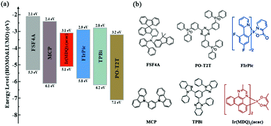 | ||
| Fig. 1 The organic materials used in this work (a) energy level diagram and (b) chemical structures. | ||
The photoluminescence (PL) spectra of FSF4A, PO-T2T (solution), TPBi, FSF4A![[thin space (1/6-em)]](https://www.rsc.org/images/entities/char_2009.gif) :
:![[thin space (1/6-em)]](https://www.rsc.org/images/entities/char_2009.gif) PO-T2T (molar ratio of 1
PO-T2T (molar ratio of 1![[thin space (1/6-em)]](https://www.rsc.org/images/entities/char_2009.gif) :
:![[thin space (1/6-em)]](https://www.rsc.org/images/entities/char_2009.gif) 1) and FSF4A
1) and FSF4A![[thin space (1/6-em)]](https://www.rsc.org/images/entities/char_2009.gif) :
:![[thin space (1/6-em)]](https://www.rsc.org/images/entities/char_2009.gif) TPBi (molar ratio of 1
TPBi (molar ratio of 1![[thin space (1/6-em)]](https://www.rsc.org/images/entities/char_2009.gif) :
:![[thin space (1/6-em)]](https://www.rsc.org/images/entities/char_2009.gif) 1) are depicted in Fig. 2(a and b). As can been seen, the PL emission spectra (films measured at 300 K) of FSF4A, PO-T2T (solution) and FSF4A
1) are depicted in Fig. 2(a and b). As can been seen, the PL emission spectra (films measured at 300 K) of FSF4A, PO-T2T (solution) and FSF4A![[thin space (1/6-em)]](https://www.rsc.org/images/entities/char_2009.gif) :
:![[thin space (1/6-em)]](https://www.rsc.org/images/entities/char_2009.gif) PO-T2T mixed film (1
PO-T2T mixed film (1![[thin space (1/6-em)]](https://www.rsc.org/images/entities/char_2009.gif) :
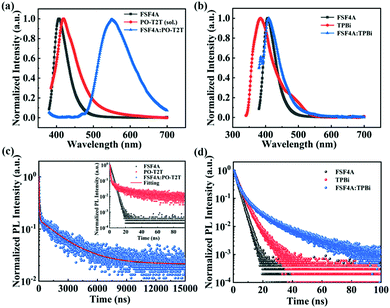
:![[thin space (1/6-em)]](https://www.rsc.org/images/entities/char_2009.gif) 1, molar ratio) are completely different, and the PL emission peak position of the FSF4A:PO-T2T film is 549 nm, which is obviously red-shifted relative to those of the pure FSF4A or PO-T2T (i.e., 407 nm for FSF4A and 419 nm for PO-T2T). The PL spectrum of the FSF4A:PO-T2T mixed film also exhibits a full width at half maximum of 103 nm, and it is highly shifted to the long wavelength region due to its intermolecular charge transfer (CT) characteristics.35 The exciplex photon energy of FSF4A:PO-T2T can be estimated to be 2.25 eV by the emission peak of the mixed film. The value is quite close to the difference (2.1 eV) between the HOMO of FSF4A (donor) and the LUMO of PO-T2T (acceptor). The results indicate that an exciplex is formed between the FSF4A molecule and the PO-T2T molecule under photo excitation, and the FSF4A:PO-T2T mixed film generates a pure CT exciplex emission. The PL emission spectrum of the peak position of the FSF4A
1, molar ratio) are completely different, and the PL emission peak position of the FSF4A:PO-T2T film is 549 nm, which is obviously red-shifted relative to those of the pure FSF4A or PO-T2T (i.e., 407 nm for FSF4A and 419 nm for PO-T2T). The PL spectrum of the FSF4A:PO-T2T mixed film also exhibits a full width at half maximum of 103 nm, and it is highly shifted to the long wavelength region due to its intermolecular charge transfer (CT) characteristics.35 The exciplex photon energy of FSF4A:PO-T2T can be estimated to be 2.25 eV by the emission peak of the mixed film. The value is quite close to the difference (2.1 eV) between the HOMO of FSF4A (donor) and the LUMO of PO-T2T (acceptor). The results indicate that an exciplex is formed between the FSF4A molecule and the PO-T2T molecule under photo excitation, and the FSF4A:PO-T2T mixed film generates a pure CT exciplex emission. The PL emission spectrum of the peak position of the FSF4A![[thin space (1/6-em)]](https://www.rsc.org/images/entities/char_2009.gif) :
:![[thin space (1/6-em)]](https://www.rsc.org/images/entities/char_2009.gif) TPBi film (1
TPBi film (1![[thin space (1/6-em)]](https://www.rsc.org/images/entities/char_2009.gif) :
:![[thin space (1/6-em)]](https://www.rsc.org/images/entities/char_2009.gif) 1, molar ratio) at 409 nm and 385 nm is depicted in Fig. 2b, which is quite similar to those of pure FSF4A (407 nm) and TPBi (385 nm) films. Thus, we infer that the mixed film of FSF4A:TPBi cannot form exciplex emission. The formation process of the exciplex can be described as the following eqn (1)36
1, molar ratio) at 409 nm and 385 nm is depicted in Fig. 2b, which is quite similar to those of pure FSF4A (407 nm) and TPBi (385 nm) films. Thus, we infer that the mixed film of FSF4A:TPBi cannot form exciplex emission. The formation process of the exciplex can be described as the following eqn (1)36
| Donor (D) + Acceptor (A) + hν → D* + A or D + A* → (Dδ+Aδ−)* → hνexciplex + D + A | (1) |
In order to further confirm the formation of exciplex in the FSF4A:PO-T2T mixed film and the absence of exciplex in the FSF4A:TPBi mixed film, the transient decay PL curves are measured at 300 K. The transient decay curves of FSF4A, PO-T2T and FSF4A:PO-T2T mixed films are depicted in Fig. 2c. The FSF4A film shows transient PL decay time components of 2.65 ns, and that of the PO-T2T film exhibits two decay components with times of 0.85 ns and 18.92 ns. Obviously different from the films of donor and acceptor molecules, the mixed film of FSF4A:PO-T2T contains a long-lived delayed component with a decay time of 2.45 μs and a short decay time of 37.53 ns. Furthermore, the short decay time of 37.53 ns in the mixed film can be attributed to the prompt fluorescence of the FSF4A:PO-T2T exciplex, rather than the separate FSF4A and PO-T2T. The long decay time of 2.45 us can be attributed to the delayed fluorescence of the FSF4A:POT2T exciplex.37 Meanwhile, the fitting formula for the tested data of the exciplex is as follows:
I(t) = A1![[thin space (1/6-em)]](https://www.rsc.org/images/entities/char_2009.gif) exp(−t/τ1) + A2 exp(−t/τ1) + A2![[thin space (1/6-em)]](https://www.rsc.org/images/entities/char_2009.gif) exp(−t/τ2) exp(−t/τ2) | (2) |
ΔEST = RT![[thin space (1/6-em)]](https://www.rsc.org/images/entities/i_char_2009.gif) ln(Keq/3) ln(Keq/3) | (3) |
 | (4) |
 | (5) |
| KISC = Kp × (1 − ΦPF) | (6) |
 | (7) |
![[thin space (1/6-em)]](https://www.rsc.org/images/entities/char_2009.gif) :
:![[thin space (1/6-em)]](https://www.rsc.org/images/entities/char_2009.gif) 5). Thus, the exciplex system can be realized by effectively converting the triplet CT into singlet CT through the reverse intersystem crossing (RISC). Fig. 2d shows the transient decay curve of the mixed film FSF4A:TPBi, which has a significantly shorter exciton lifetime compared to FSF4A:PO-T2T. These results further support the formation of FSF4A:PO-T2T exciplex emission, while FSF4A:TPBi cannot form exciplex emission.
5). Thus, the exciplex system can be realized by effectively converting the triplet CT into singlet CT through the reverse intersystem crossing (RISC). Fig. 2d shows the transient decay curve of the mixed film FSF4A:TPBi, which has a significantly shorter exciton lifetime compared to FSF4A:PO-T2T. These results further support the formation of FSF4A:PO-T2T exciplex emission, while FSF4A:TPBi cannot form exciplex emission.
To investigate the EL characteristics of the FSF4A:PO-T2T exciplex, an OLED is fabricated with the exciplex as the emission layer (EML) by the structure of ITO/MoO3 (2 nm)/FSF4A (45 nm)/FSF4A:PO-T2T (20 nm)/PO-T2T (35 nm)/Liq (1 nm)/Al (100 nm). The ratio of FSF4A![[thin space (1/6-em)]](https://www.rsc.org/images/entities/char_2009.gif) :
:![[thin space (1/6-em)]](https://www.rsc.org/images/entities/char_2009.gif) PO-T2T is 3
PO-T2T is 3![[thin space (1/6-em)]](https://www.rsc.org/images/entities/char_2009.gif) :
:![[thin space (1/6-em)]](https://www.rsc.org/images/entities/char_2009.gif) 7, 5
7, 5![[thin space (1/6-em)]](https://www.rsc.org/images/entities/char_2009.gif) :
:![[thin space (1/6-em)]](https://www.rsc.org/images/entities/char_2009.gif) 5, and 7
5, and 7![[thin space (1/6-em)]](https://www.rsc.org/images/entities/char_2009.gif) :
:![[thin space (1/6-em)]](https://www.rsc.org/images/entities/char_2009.gif) 3, respectively. As exhibited in Fig. 3(a–c), the device based on the exciplex emission layer with a mixing ratio of 5
3, respectively. As exhibited in Fig. 3(a–c), the device based on the exciplex emission layer with a mixing ratio of 5![[thin space (1/6-em)]](https://www.rsc.org/images/entities/char_2009.gif) :
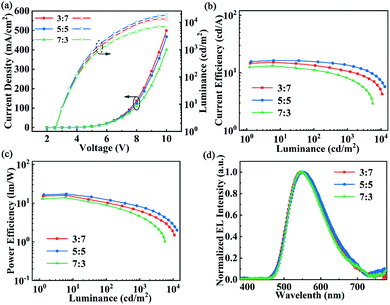
:![[thin space (1/6-em)]](https://www.rsc.org/images/entities/char_2009.gif) 5 can achieve the maximum luminance (Lmax) of 18513 cd m−2, the maximum CE of 16.4 cd A−1 and the maximum PE of 17.2 lm W−1 with an ultralow turn-on voltage of 2.4 V. Detailed characteristics are summarized in Table 1. The low turn-on voltage and high performance can be attributed to the “barrier-free” device structure, that is, holes and electrons can be injected into EML from FSF4A and PO-T2T without barrier, respectively.39 Meanwhile, the device with the FSF4A
5 can achieve the maximum luminance (Lmax) of 18513 cd m−2, the maximum CE of 16.4 cd A−1 and the maximum PE of 17.2 lm W−1 with an ultralow turn-on voltage of 2.4 V. Detailed characteristics are summarized in Table 1. The low turn-on voltage and high performance can be attributed to the “barrier-free” device structure, that is, holes and electrons can be injected into EML from FSF4A and PO-T2T without barrier, respectively.39 Meanwhile, the device with the FSF4A![[thin space (1/6-em)]](https://www.rsc.org/images/entities/char_2009.gif) :
:![[thin space (1/6-em)]](https://www.rsc.org/images/entities/char_2009.gif) PO-T2T mixing ratio of 5
PO-T2T mixing ratio of 5![[thin space (1/6-em)]](https://www.rsc.org/images/entities/char_2009.gif) :
:![[thin space (1/6-em)]](https://www.rsc.org/images/entities/char_2009.gif) 5 achieves the greatest luminance and efficiency, which is due to a more balanced carrier transport. Therefore, all the OLEDs based on FSF4A
5 achieves the greatest luminance and efficiency, which is due to a more balanced carrier transport. Therefore, all the OLEDs based on FSF4A![[thin space (1/6-em)]](https://www.rsc.org/images/entities/char_2009.gif) :
:![[thin space (1/6-em)]](https://www.rsc.org/images/entities/char_2009.gif) PO-T2T emitting were developed with the optimized molar ratio of 5
PO-T2T emitting were developed with the optimized molar ratio of 5![[thin space (1/6-em)]](https://www.rsc.org/images/entities/char_2009.gif) :
:![[thin space (1/6-em)]](https://www.rsc.org/images/entities/char_2009.gif) 5. Fig. 3d shows the electroluminescence spectra of different ratios of exciplex as the emitting layer device. The emission peak position of the device with a mixing ratio of 5
5. Fig. 3d shows the electroluminescence spectra of different ratios of exciplex as the emitting layer device. The emission peak position of the device with a mixing ratio of 5![[thin space (1/6-em)]](https://www.rsc.org/images/entities/char_2009.gif) :
:![[thin space (1/6-em)]](https://www.rsc.org/images/entities/char_2009.gif) 5 is 550 nm at the voltage of 6 V, which is extremely consistent with the photoluminescence peak. The energy transfer characteristics of the FSF4A:PO-T2T exciplex should be considered when it is used as the host: (1) a higher LUMO of FSF4A and a deeper HOMO of PO-T2T limit the exciton recombination zone to avoid quenching during charge transport. (2) The T1 level of FSF4A and PO-T2T is higher than the T1 level of the exciplex to effectively restrain the exciton energy transfer to the consisting donor or acceptor. (3) The exciplex needs to have a higher T1 level than phosphorescent dopants to restrain energy transfer from the phosphors to the exciplex.28,29 According to the PL spectrum (S1 = 2.258 eV) and ΔEst (0.022 eV) of the exciplex, T1 can be estimated to be about 2.236 eV, which is obviously lower than FSF4A (2.6 eV) and PO-T2T (3.0 eV).40 Therefore, the red dye Ir(MDQ)2acac (2.0 eV) is used as a dopant to design red PhOLEDs based on the characteristics of a novel exciplex co-host.31
5 is 550 nm at the voltage of 6 V, which is extremely consistent with the photoluminescence peak. The energy transfer characteristics of the FSF4A:PO-T2T exciplex should be considered when it is used as the host: (1) a higher LUMO of FSF4A and a deeper HOMO of PO-T2T limit the exciton recombination zone to avoid quenching during charge transport. (2) The T1 level of FSF4A and PO-T2T is higher than the T1 level of the exciplex to effectively restrain the exciton energy transfer to the consisting donor or acceptor. (3) The exciplex needs to have a higher T1 level than phosphorescent dopants to restrain energy transfer from the phosphors to the exciplex.28,29 According to the PL spectrum (S1 = 2.258 eV) and ΔEst (0.022 eV) of the exciplex, T1 can be estimated to be about 2.236 eV, which is obviously lower than FSF4A (2.6 eV) and PO-T2T (3.0 eV).40 Therefore, the red dye Ir(MDQ)2acac (2.0 eV) is used as a dopant to design red PhOLEDs based on the characteristics of a novel exciplex co-host.31
| Mixing ratio | V on [V) | L max [cd m−2] | CEc [cd A−1] | PEc [lm W−1] | EQEc [%] | λ EL [nm] | CIEe [x,y] |
|---|---|---|---|---|---|---|---|
| a Turn-on voltage at a luminance of 1 cd m−2. b Maximum brightness value. c Maximum CE, current efficiency; PE, power efficiency; EQE, external quantum efficiency. d Electroluminescence emission peak. e CIE coordinate is measured at 1000 cd m−2. | |||||||
3![[thin space (1/6-em)]](https://www.rsc.org/images/entities/char_2009.gif) : :![[thin space (1/6-em)]](https://www.rsc.org/images/entities/char_2009.gif) 7 7 |
2.40 | 13![[thin space (1/6-em)]](https://www.rsc.org/images/entities/char_2009.gif) 192 192 |
15.2 | 15.9 | 5.87 | 550 | 0.41,0.54 |
5![[thin space (1/6-em)]](https://www.rsc.org/images/entities/char_2009.gif) : :![[thin space (1/6-em)]](https://www.rsc.org/images/entities/char_2009.gif) 5 5 |
2.40 | 18![[thin space (1/6-em)]](https://www.rsc.org/images/entities/char_2009.gif) 513 513 |
16.4 | 17.2 | 6.48 | 550 | 0.41,0.54 |
7![[thin space (1/6-em)]](https://www.rsc.org/images/entities/char_2009.gif) : :![[thin space (1/6-em)]](https://www.rsc.org/images/entities/char_2009.gif) 3 3 |
2.40 | 7033 | 13.2 | 13.8 | 4.76 | 548 | 0.41,0.54 |
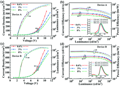
The red PhOLEDs are prepared in the structures of ITO/MoO3 (2 nm)/FSF4A (45 nm)/FSF4A:PO-T2T: x wt% Ir(MDQ)2acac (20 nm)/PO-T2T (35 nm)/Liq (1 nm)/Al (100 nm) and comparative device structure of ITO/MoO3 (2 nm)/FSF4A (45 nm)/FSF4A:TPBi: x wt% Ir(MDQ)2acac (20 nm)/TPBi (35 nm)/Liq (1 nm)/Al (100 nm), in which the mixing ratios of the FSF4A:PO-T2T exciplex co-host and FSF4A![[thin space (1/6-em)]](https://www.rsc.org/images/entities/char_2009.gif) :
:![[thin space (1/6-em)]](https://www.rsc.org/images/entities/char_2009.gif) TPBi common co-host are 1
TPBi common co-host are 1![[thin space (1/6-em)]](https://www.rsc.org/images/entities/char_2009.gif) :
:![[thin space (1/6-em)]](https://www.rsc.org/images/entities/char_2009.gif) 1 corresponding to devices A and B, and the doping concentration of the red dye Ir(MDQ)2acac is 0.6%, 3%, and 8% corresponding to devices A1–A3 and B1–B3, respectively. As can be seen from Fig. 4a, device A2 (3 wt% Ir(MDQ)2acac) displays an extremely low turn-on voltage of 1.95 V and a maximum brightness of 35490 cd m−2. The maximum CE, PE, and EQE of 30.6 cd A−1, 38.5 lm W−1, and 17.3% are shown in Fig. 4b, and the inset shows the emission peak at 616 nm with CIE coordinates of (0.61,0.37). It is encouraging that the turn-on voltage of A1–A3 is extremely low at 1.95 V, which is even 0.05 V lower than the theoretical limit voltage corresponding to the emission photon energy of Ir(MDQ)2acac (2.0 eV). The extremely low turn-on voltage is due to the fact that the thermally activated carriers.43 Such low turn-on voltage and high efficiency are a great improvement compared with previous reported red OLEDs based on the exciplex co-host (Table 2). Fig. 4c shows that device B2 (with a doping concentration of 3 wt% Ir(MDQ)2acac) achieves a low turn-on voltage of 2.55 V and a maximum brightness of 24410 cd m−2. The maximum CE, PE, and EQE are 25.7 cd A−1, 26.9 lm W−1, and 11.9%, which can be seen in Fig. 4d, and the inset displays the emission peak at 612 nm with CIE coordinates of (0.61,0.37). As can be seen, the device employing the FSF4A:PO-T2T exciplex co-host exhibits superior electroluminescence performance compared to the device employing the FSF4A:TPBi common co-host. The EL performance of device A2 and B2 confirms the superiority of the exciplex as co-host in achieving ultralow turn-on voltage and high efficiency, which may be attributed to the carriers being more likely to cross the barrier and the excitons being effectively transferred to the dopant. It is also noticed that the J–V–L and CE–L–PE characteristics exhibited by device A and B with varied Ir(MDQ)2acac doping concentrations are quite different, as shown in Fig. 4. Detailed characteristics for device A1–A3 and B1–B3 are summarized in Table 3.
1 corresponding to devices A and B, and the doping concentration of the red dye Ir(MDQ)2acac is 0.6%, 3%, and 8% corresponding to devices A1–A3 and B1–B3, respectively. As can be seen from Fig. 4a, device A2 (3 wt% Ir(MDQ)2acac) displays an extremely low turn-on voltage of 1.95 V and a maximum brightness of 35490 cd m−2. The maximum CE, PE, and EQE of 30.6 cd A−1, 38.5 lm W−1, and 17.3% are shown in Fig. 4b, and the inset shows the emission peak at 616 nm with CIE coordinates of (0.61,0.37). It is encouraging that the turn-on voltage of A1–A3 is extremely low at 1.95 V, which is even 0.05 V lower than the theoretical limit voltage corresponding to the emission photon energy of Ir(MDQ)2acac (2.0 eV). The extremely low turn-on voltage is due to the fact that the thermally activated carriers.43 Such low turn-on voltage and high efficiency are a great improvement compared with previous reported red OLEDs based on the exciplex co-host (Table 2). Fig. 4c shows that device B2 (with a doping concentration of 3 wt% Ir(MDQ)2acac) achieves a low turn-on voltage of 2.55 V and a maximum brightness of 24410 cd m−2. The maximum CE, PE, and EQE are 25.7 cd A−1, 26.9 lm W−1, and 11.9%, which can be seen in Fig. 4d, and the inset displays the emission peak at 612 nm with CIE coordinates of (0.61,0.37). As can be seen, the device employing the FSF4A:PO-T2T exciplex co-host exhibits superior electroluminescence performance compared to the device employing the FSF4A:TPBi common co-host. The EL performance of device A2 and B2 confirms the superiority of the exciplex as co-host in achieving ultralow turn-on voltage and high efficiency, which may be attributed to the carriers being more likely to cross the barrier and the excitons being effectively transferred to the dopant. It is also noticed that the J–V–L and CE–L–PE characteristics exhibited by device A and B with varied Ir(MDQ)2acac doping concentrations are quite different, as shown in Fig. 4. Detailed characteristics for device A1–A3 and B1–B3 are summarized in Table 3.
| V on [V] | L max [cd m−2] | CEmaxc [cd A−1] | PEmaxd [lm W−1] | EQEmaxe [%] | |
|---|---|---|---|---|---|
| a Turn-on voltage at a luminance of 1 cd m−2. b Maximum brightness value. c Maximum CE, current efficiency. d Maximum PE, power efficiency. e Maximum EQE, external quantum efficiency. | |||||
| This work | 1.95 | 35![[thin space (1/6-em)]](https://www.rsc.org/images/entities/char_2009.gif) 490 490 |
30.6 | 38.5 | 17.3 |
| 30 | 2.4 | 26![[thin space (1/6-em)]](https://www.rsc.org/images/entities/char_2009.gif) 385 385 |
31.1 | 36.9 | 15.5 |
| 41 | 2.35 | 7694 | 34.0 | 44.3 | 19.2 |
| 31 | 1.90 | — | — | 48.9 | 26.8 |
| 29 | 2.24 | — | 32.87 | 31.80 | 11.01 |
| 42 | 2.4 | — | 36.0 | 46.1 | 24.5 |
| 38 | 2.0 | — | 30.13 | 42.75 | 16.07 |
| 28 | 2.6 | 33![[thin space (1/6-em)]](https://www.rsc.org/images/entities/char_2009.gif) 560 560 |
33.9 | 35.3 | 19.8 |
| Device | Doping concentrationa (%) | V on [V] | CEmax/1000/3000c [cd A−1] | PEmax/1000/3000d [lm W-1] | EQEmax/1000/3000e [%] | CIEf [x,y] |
|---|---|---|---|---|---|---|
| a Doping concentration of Ir(MDQ)2acac. b Turn-on voltage at a luminance of 1 cd m−2. c The maximum current efficiency/current efficiency at 1000 cd m−2/current efficiency at 3000 cd m−2. d The maximum power efficiency/power efficiency at 1000 cd m−2/power efficiency at 3000 cd m-2. e The maximum EQE/EQE at 1000 cd m−2/EQE at 3000 cd m−2. f CIE coordinates are measured at 1000 cd m−2. | ||||||
| A1 | 0.6 | 1.95 | 26.6/23.3/18.3 | 33.4/18.0/10.3 | 15.2/11.1/9.6 | (0.56,0.42) |
| A2 | 3 | 1.95 | 30.6/26.0/21.7 | 38.5/20.4/12.4 | 17.3/12.8/10.4 | (0.61,0.37) |
| A3 | 8 | 1.95 | 22.6/18.9/16.6 | 28.4/13.2/8.7 | 13.8/7.9/5.9 | (0.64,0.35) |
| B1 | 0.6 | 2.55 | 23.1/21.1/17.7 | 24.2/14.7/10.1 | 10.7/8.4/6.5 | (0.57,0.37) |
| B2 | 3 | 2.55 | 25.7/24.7/19.5 | 26.9/19.4/11.1 | 11.9/10.7/8.2 | (0.61,0.37) |
| B3 | 8 | 2.55 | 20.6/17.6/15.0 | 21.5/12.3/8.6 | 9.6/7.6/5.7 | (0.62,0.36) |
It can be seen from the insets that the host emission peaks exist only at a low doping concentration of 0.6% Ir(MDQ)2acac, which can be explained as an incomplete energy transfer from the host to the dopant. The EL efficiency declined as the doping concentration of Ir(MDQ)2acac increases to 8%, which is due to the strengthening of triplet–triplet annihilation, and triplet-polaron quenching with a higher proportion of dye. Meanwhile, a slight red shift with increasing doping concentration can be observed in the insets of Fig. 4(b and d), which is due to reabsorption of the emitter emission. Based on the above results, it is confirmed that the FSF4A:PO-T2T exciplex co-host doped with 3% Ir(MDQ)2acac concentration achieves the optimal EL efficiency.
To further understand the effect of dopant on the charge transport properties of the device, we subsequently research the charge transport properties by varying the doping concentration of hole-only and electron-only devices with the structures of ITO/MoO3 (2 nm)/FSF4A (45 nm)/FSF4A:PO-T2T: x wt% Ir(MDQ)2acac (20 nm)/FSF4A (35nm)/MoO3 (1 nm)/Al and ITO/Liq (1 nm)/PO-T2T (45 nm)/FSF4A:PO-T2T: x wt% Ir(MDQ)2acac (20 nm)/PO-T2T (35 nm)/Liq (1 nm)/Al, respectively. Here x is 0, 0.6, 3, and 8. Fig. 5 exhibits the current density–voltage characteristics of these devices. Obviously we can notice that the charge carrier transmission of the device tends to be more balanced as the doping concentration of Ir(MDQ)2acac is increased from 0% to 8%, it is due to the fact that Ir(MDQ)2acac has a strong hole trap effect and creates an additional electron transport channel. Ir(MDQ)2acac has the highest occupied molecular orbital energy level of 5.1 eV, which is a 0.2 eV difference to that of FSF4A (5.3 eV), indicating that Ir(MDQ)2acac acts as trapping sites for holes. On the contrary, the current density of electron-only devices increases with increasing the doping concentration of Ir(MDQ)2acac. The improvement can be attributed to the fact the Ir(MDQ)2acac molecules create an additional electron transport channel, which is beneficial for more balanced charge carriers in the devices. Overall, it is found that doping Ir(MDQ)2acac into an exciplex co-host can simultaneously trap holes and facilitate electron transport. Both of these processes lead to more balanced charge carriers, which causes a slight shift of the recombination zone to the center of the device.44
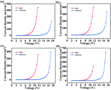 | ||
| Fig. 5 The current density–voltage characteristics of (a) 0% Ir(MDQ)2acac, (b) 0.6% Ir(MDQ)2acac, (c) 3% Ir(MDQ)2acac, and (d) 8% Ir(MDQ)2acac. | ||
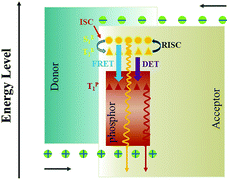
The energy transfer mechanism of red OLEDs based on the exciplex co-host is illustrated in Fig. 6. Excitons are produced by the direct recombination between holes on the donor (FSF4A) and electrons on the acceptor (PO-T2T), the exciplex excitons can also be divided into singlet excitons of 25% and triplet excitons of 75%. For singlet excitons of the exciplex, one is converted to triplet excitons by intersystem crossing, and the other is to transfer energy to the dopant by Förster energy transfer (FRET); for triplet excitons of the exciplex, part of which can diffuse into the dopant through Dexter energy transfer (DET), but the triplet energy is lost as the diffusion length increases.45 Meanwhile, another triplet could upconvert into the singlet by the reverse intersystem crossing due to the small ΔEst of the exciplex. This process can effectively reduce energy loss due to improving FRET energy transfer and suppressing DET energy transfer. Therefore, we can achieve efficient and stable exciplex co-host PhOLEDs.
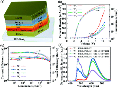
Based on the above excellent monochrome devices, ultra-thin blue layers and spacer-layers are inserted to achieve high-performance WOLEDs, and the device structure is ITO/MoO3 (2 nm)/FSF4A (45 nm)/FSF4A:PO-T2T: 3 wt% Ir(MDQ)2acac (20 nm)/MCP (x nm)/FIrPic (0.2 nm)/PO-T2T (35 nm)/Liq (1 nm)/Al (100 nm), as shown in Fig. 7a. The x is 1, 2, 3 and 4, corresponding to devices W1, W2, W3 and W4, respectively. As can be seen from Fig. 7b, all WOLEDs realize an ultra-low turn-on voltage of 2.20 V due to the barrier-free charge transfer. The current density of the four devices decreases as the thickness of the spacer layer increases, which can be explained by the following formula (J–V curves):52
 | (8) |
| V on [V] | L [cd m−2] | CEc [cd A−1] | PEc [lm W−1] | EQEc [%] | CIEd [x,y] | CRI | |
|---|---|---|---|---|---|---|---|
| a Turn-on voltage at a luminance of 1 cd m−2. b Maximum brightness value. c Maximum CE, PE, and EQE. d The CIE coordinates at 1000 cd m−2. | |||||||
| This work | 2.20 | 14![[thin space (1/6-em)]](https://www.rsc.org/images/entities/char_2009.gif) 420 420 |
32.6 | 34.1 | 12.4 | (0.33,0.33) | 52 |
| 46 | 4.43 | — | 28.0 | 20.2 | 12.0 | (0.33,0.33) | 83 |
| 47 | — | — | 23.1 | 15.6 | 13.5 | (0.33,0.34) | 59 |
| 48 | 3.20 | 19![[thin space (1/6-em)]](https://www.rsc.org/images/entities/char_2009.gif) 200 200 |
10.7 | 8.1 | 6.4 | (0.33.0.33) | — |
| 49 | 2.62 | — | 44.0 | 52.7 | 19.0 | (0.34,0.35) | 72.2 |
| 24 | 3.0 | — | 36.50 | 37.31 | 13.39 | (0.35,0.39) | 78 |
| 50 | — | — | 27.2 | 21.4 | 11.2 | (0.35.0.39) | 66 |
| 51 | 2.5 | — | 36.7 | 46.2 | 19.2 | (0.33,0.38) | 82 |
| Device | V on [V] | CE [cd A−1]max/1000/3000 | PE [lm W−1]max/1000/3000 | EQE [%]max/1000/3000 | Roll-offa (%) | CIEb [x,y] | ΔCIEc [x,y] |
|---|---|---|---|---|---|---|---|
| a The CE roll-off at 1000 cd m−2. b The CIE coordinates at 1000 cd m−2. c The CIE coordinate variation from 4 to 7 V. | |||||||
| W1 | 2.20 | 23.9/23.3/20.7 | 25.1/15.7/10.2 | 10.7/9.4/8.2 | 2.5 | (0.589,0.379) | (0.012,0.002) |
| W2 | 2.20 | 27.1/24.9/22.5 | 28.5/17.2/12.1 | 11.0/9.8/8.4 | 8.1 | (0.478,0.362) | (0.026,0.004) |
| W3 | 2.20 | 29.5/26.4/23.9 | 30.5/18.4/13.0 | 11.6/10.0/8.6 | 10.5 | (0.403,0.351) | (0.028,0.003) |
| W4 | 2.20 | 32.6/30.3/25.1 | 34.1/21.4/13.6 | 12.4/10.6/9.1 | 7.1 | (0.333.0.337) | (0.026,0.003) |
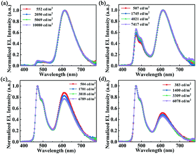
Fig. 8 exhibits the normalized EL spectra of devices W1–W4 at different luminance. The device W1 shows a rather weak blue emission, which can be attributed to the strong energy transfer due to the thinner spacer layer. Obviously, for white devices W2, W3, and W4, the relatively stable spectra are displayed in a large luminance range with a slight CIE coordinate shift. The CIE coordinate shift of device W2–W4 is from (0.488,0.366), (0.414,0.353), and (0.352,0.343) at 4V to (0.462,0.362), (0.386,0.350), and (0.326,0.340) at 7V, revealing the CIE variation is only (0.026,0.004), (0.028, 0.003), and (0.026, 0.003), respectively. The only slight colour shift in the EL spectra may be attributed to the bipolarity of the exciplex co-host, which reduces the recombination zone movement. Meanwhile, as the thickness of the spacer layer increases, the colour rending index of devices W2–W4 sequentially decreases, which is due to the gradual decrease of the red emission peak.
4. Conclusions
In summary, we have successfully achieved ultralow turn-on voltage, high-performance simplified red and white phosphorescent OLEDs based on a novel exciplex co-host. The energy transfer from the exciplex co-host to its constituents is completely suppressed due to the high ET of both FSF4A and PO-T2T, while from the host to the dopant is improved through long-range Förster energy transfer. The red device implements an ultra-low turn-on voltage of 1.95 V and the maximum EQE of 17.3% under a low doping level of 3 wt%, which is due to barrier-free charge transfer and effective energy transfer. Meanwhile, white OLEDs with a low turn-on voltage of 2.2 V is realized based on doping red dye and inserting an ultra-thin blue layer, the optimized device shows relatively stable spectra and low efficiency roll-off. These superior performances can be attributed to the balanced charge transfer of the exciplex co-host and the effective energy transfer from the exciplex co-host to the dopant. Such results indicate a promising method for designing simplified high-performance OLEDs.Conflicts of interest
There are no conflicts to declare.Acknowledgements
The work was funded by the Project of Science and Technology Development Plan of Jilin Province (20190302011GX) and the National Natural Science Foundation of China (61675088 and 61675089).References
- X. Cai, R. Liu, H. Shi, C. Li and H. Zhu, Dyes Pigm., 2017, 143, 196–202 CrossRef CAS.
- K. Gao, K. Liu, X.-L. Li, X. Cai, D. Chen, Z. Xu, Z. He, B. Li, Z. Qiao, D. Chen, Y. Cao and S.-J. Su, J. Mater. Chem. C, 2017, 5(39), 10406–10416 RSC.
- C. Adachi, R. C. Kwong, P. Djurovich, V. Adamovich, M. A. Baldo, M. E. Thompson and S. R. Forrest, Appl. Phys. Lett., 2001, 79(13), 2082–2084 CrossRef CAS.
- Y. J. Cho, K. S. Yook and J. Y. Lee, Sci. Rep., 2015, 5, 7859 CrossRef CAS PubMed.
- N. Sun, Q. Wang, Y. Zhao, Y. Chen, D. Yang, F. Zhao, J. Chen and D. Ma, Adv. Mater., 2014, 26(10), 1617–1621 CrossRef CAS PubMed.
- B. Q. Liu, L. Wang, D. Y. Gao, J. H. Zou, H. L. Ning, J. B. Peng and Y. Cao, Light: Sci. Appl., 2016, 5(8), e16137 CrossRef CAS PubMed.
- L. Jia, L. Jin, K. Yuan, L. Chen, J. Yuan, S. Xu, W. Lv and R. Chen, ACS Sustainable Chem. Eng., 2018, 6(7), 8809–8815 CrossRef CAS.
- P. Chen, R. Sheng, M.-Y. Ko, Y. Duan, G. Cheng and C.-M. Che, J. Mater. Chem. C, 2018, 6(37), 9890–9896 RSC.
- S. Ying, J. Yao, Y. Chen and D. Ma, J. Mater. Chem. C, 2018, 6(26), 7070–7076 RSC.
- X. Liao, K. An, J. Cheng, Y. Li, X. Meng, X. Yang and L. Li, Appl. Surf. Sci., 2019, 487, 610–615 CrossRef CAS.
- J. Zhao, S. Yuan, X. Du, W. Li, C. Zheng, S. Tao and X. Zhang, Adv. Opt. Mater., 2018, 6(23), 1800825 CrossRef.
- R. J. Holmes, S. R. Forrest, Y. J. Tung, R. C. Kwong, J. J. Brown, S. Garon and M. E. Thompson, Appl. Phys. Lett., 2003, 82(15), 2422–2424 CrossRef CAS.
- M.-S. Lin, S.-J. Yang, H.-W. Chang, Y.-H. Huang, Y.-T. Tsai, C.-C. Wu, S.-H. Chou, E. Mondal and K.-T. Wong, J. Mater. Chem., 2012, 22(31), 16114–16120 RSC.
- H. Mu, Y. Jiang and H. Xie, Org. Electron., 2019, 66, 195–205 CrossRef CAS.
- Z. Wang, C. Wang, H. Zhang, Z. Liu, B. Zhao and W. Li, Org. Electron., 2019, 66, 227–241 CrossRef CAS.
- H.-Y. Yang, C.-J. Zheng, M. Zhang, J.-W. Zhao, P.-L. Zhong, H. Lin, S.-L. Tao and X.-H. Zhang, Org. Electron., 2019, 73, 36–42 CrossRef CAS.
- W. Zeng, T. Zhou, W. Ning, C. Zhong, J. He, S. Gong, G. Xie and C. Yang, Adv. Mater., 2019, 31(33), e1901404 CrossRef PubMed.
- S. Yuan, X. Du, J. Zhao, W. Liu, H. Lin, C. Zheng, S. Tao and X. Zhang, Org. Electron., 2016, 39, 10–15 CrossRef CAS.
- P. Chen, B. Chen, L. Zuo, Y. Duan, G. Han, R. Sheng, K. Xue and Y. Zhao, Org. Electron., 2016, 31, 136–141 CrossRef CAS.
- T.-C. Liao, H.-T. Chou, F.-S. Juang, Y.-S. Tsai, L.-A. Hong and Y.-Y. Ho, Curr. Appl. Phys., 2013, 13, S152–S155 CrossRef.
- K.-H. Kim, S.-J. Yoo and J.-J. Kim, Chem. Mater., 2016, 28(6), 1936–1941 CrossRef CAS.
- C. J. Zheng, J. Wang, J. Ye, M. F. Lo, X. K. Liu, M. K. Fung, X. H. Zhang and C. S. Lee, Adv. Mater., 2013, 25(15), 2205–2211 CrossRef CAS PubMed.
- P. Yuan, X. Qiao, D. Yan and D. Ma, J. Mater. Chem. C, 2018, 6(21), 5721–5726 RSC.
- Y. Liu, X. Wei, Z. Li, J. Liu, R. Wang, X. Hu, P. Wang, T. Qi and Y. Wang, Adv. Opt. Mater., 2018, 6(23), 1800978 CrossRef.
- F. Yan, R. Chen, H. Sun and X. Wei Sun, Appl. Phys. Lett., 2014, 104(15), 153302 CrossRef.
- Y. Seino, H. Sasabe, Y. J. Pu and J. Kido, Adv. Mater., 2014, 26(10), 1612–1616 CrossRef CAS PubMed.
- B. Zhao, Y. Miao, Z. Wang, W. Chen, K. Wang, H. Wang, Y. Hao, B. Xu and W. Li, Org. Electron., 2016, 37, 1–5 CrossRef.
- R. Sheng, A. Li, F. Zhang, J. Song, Y. Duan and P. Chen, Adv. Opt. Mater., 2020, 8(2), 1901247 CrossRef CAS.
- T. Xu, Y. X. Zhang, B. Wang, C. C. Huang, I. Murtaza, H. Meng and L. S. Liao, ACS Appl. Mater. Interfaces, 2017, 9(3), 2701–2710 CrossRef CAS PubMed.
- B. Yao, X. Lin, B. Zhang, H. Wang, X. Liu and Z. Xie, J. Mater. Chem. C, 2018, 6(16), 4409–4417 RSC.
- J. H. Lee, H. Shin, J. M. Kim, K. H. Kim and J. J. Kim, ACS Appl. Mater. Interfaces, 2017, 9(4), 3277–3281 CrossRef CAS PubMed.
- Y.-L. Zhang, Q. Ran, Q. Wang, J. Fan and L.-S. Liao, J. Mater. Chem. C, 2019, 7(24), 7267–7272 RSC.
- X. Tang, X. Y. Liu, Y. Yuan, Y. J. Wang, H. C. Li, Z. Q. Jiang and L. S. Liao, ACS Appl. Mater. Interfaces, 2018, 10(35), 29840–29847 CrossRef CAS PubMed.
- D. Chen, Z. Wang, D. Wang, Y.-C. Wu, C.-C. Lo, A. Lien, Y. Cao and S.-J. Su, Org. Electron., 2015, 25, 79–84 CrossRef CAS.
- S.-F. Wu, S.-H. Li, Y.-K. Wang, C.-C. Huang, Q. Sun, J.-J. Liang, L.-S. Liao and M.-K. Fung, Adv. Funct. Mater., 2017, 27(31), 1701314 CrossRef.
- X. K. Liu, Z. Chen, C. J. Zheng, C. L. Liu, C. S. Lee, F. Li, X. M. Ou and X. H. Zhang, Adv. Mater., 2015, 27(14), 2378–2383 CrossRef CAS PubMed.
- X. K. Liu, Z. Chen, J. Qing, W. J. Zhang, B. Wu, H. L. Tam, F. Zhu, X. H. Zhang and C. S. Lee, Adv. Mater., 2015, 27(44), 7079–7085 CrossRef CAS PubMed.
- X. Liao, K. An, Y. Li, X. Meng, S. Chen, X. Yang and L. Li, Dyes Pigm., 2020, 182 Search PubMed.
- J.-H. Lee, S.-H. Cheng, S.-J. Yoo, H. Shin, J.-H. Chang, C.-I. Wu, K.-T. Wong and J.-J. Kim, Adv. Funct. Mater., 2015, 25(3), 361–366 CrossRef CAS.
- M. Colella, A. Danos and A. P. Monkman, J. Phys. Chem. C, 2019, 123(28), 17318–17324 CrossRef CAS.
- J. Zhao, X. Du, S. Yuan, C. Zheng, H. Lin and S. Tao, Org. Electron., 2017, 43, 136–141 CrossRef CAS.
- Q.-S. Tian, X.-D. Zhu and L.-S. Liao, Mater. Chem. Front., 2020, 4(6), 1648–1655 RSC.
- H. Sasabe, H. Nakanishi, Y. Watanabe, S. Yano, M. Hirasawa, Y.-J. Pu and J. Kido, Adv. Funct. Mater., 2013, 23(44), 5550–5555 CrossRef CAS.
- Y. Chen, Y. Xia, G. M. Smith, C. A. Hewitt, Q. Fu, Y. Liu, H. Sun, D. Ma, Y. Gu, C. Yang, Y. Mei and D. L. Carroll, Org. Electron., 2014, 15(1), 182–188 CrossRef CAS.
- D. Zhang, M. Cai, Y. Zhang, D. Zhang and L. Duan, ACS Appl. Mater. Interfaces, 2015, 7(51), 28693–28700 CrossRef CAS PubMed.
- W. Luo, T.-T. Wang, X. Chen, K.-N. Tong, W. He, S.-Q. Sun, Y.-J. Zhang, L.-S. Liao and M.-K. Fung, J. Mater. Chem. C, 2020, 8(30), 10431–10437 RSC.
- C.-C. Fan, M.-H. Huang, W.-C. Lin, H.-W. Lin, Y. Chi, H.-F. Meng, T.-C. Chao and M.-R. Tseng, Org. Electron., 2014, 15(2), 517–523 CrossRef CAS.
- W. Qin, Z. Yang, Y. Jiang, J. W. Y. Lam, G. Liang, H. S. Kwok and B. Z. Tang, Chem. Mater., 2015, 27(11), 3892–3901 CrossRef CAS.
- H. Sasabe, J. Takamatsu, T. Motoyama, S. Watanabe, G. Wagenblast, N. Langer, O. Molt, E. Fuchs, C. Lennartz and J. Kido, Adv. Mater., 2010, 22(44), 5003–5007 CrossRef CAS PubMed.
- D. Feng, D. Dong, L. Lian, H. Wang and G. He, Org. Electron., 2018, 56, 216–220 CrossRef CAS.
- M. Zhang, K. Wang, C.-J. Zheng, W. Liu, H. Lin, S.-L. Tao and X.-H. Zhang, Org. Electron., 2017, 50, 466–472 CrossRef CAS.
- B. Wang, Z. Kou, Y. Tang, F. Yang, X. E. Fu and Q. Yuan, Org. Electron., 2019, 70, 149–154 CrossRef CAS.
- H. Wang, D. Dong, L. Lian, F. Zhu, D. Xu, S. Wu and G. He, Phys. Status Solidi A, 2019, 216(11), 1900034 CrossRef.
| This journal is © The Royal Society of Chemistry 2021 |

