 Open Access Article
New π-stacking motifs for molecular semiconducting materials: bis(bis(8-quinolinyl)amide)metal(II) complexes of Cr, Mn, Fe, and Zn†
Georg
Albrecht‡
ab,
Harald
Locke‡
bc,
Pascal
Schweitzer‡
ab,
Jonathan
Becker
d,
Limei
Chen
be,
Peter R.
Schreiner
 *bc and
Derck
Schlettwein
 *ab
*ab
aInstitute of Applied Physics, Justus Liebig University Giessen, Heinrich-Buff-Ring 16, 35392 Giessen, Germany. E-mail: schlettwein@uni-giessen.de
bCenter for Materials Research (ZfM), Justus Liebig University Giessen, Heinrich-Buff-Ring 16, 35392 Giessen, Germany
cInstitute of Organic Chemistry, Justus Liebig University Giessen, Heinrich-Buff-Ring 17, 35392 Giessen, Germany
dInstitute of Inorganic and Analytical Chemistry, Justus Liebig University Giessen, Heinrich-Buff-Ring 17, 35392 Giessen, Germany
eInstitute for Experimental Physics I, Justus Liebig University Giessen, Heinrich-Buff-Ring 16, 35392 Giessen, Germany
First published on 2nd March 2021
Abstract
π–π stacking of adjacent molecules is an essential prerequisite for charge carrier transport in organic semiconductors. Neutral metal–organic complexes with two pincer-type bis(8-quinolinyl)amide (BQA) ligands forming orthogonal π-systems in complexes with octahedrally coordinated metal centres (Cr, Mn, Fe, Zn) were synthesized. Cr and Fe are shown to facilitate face-to-edge and parallel displaced stacking in two orthogonal directions as evident from single crystal X-ray diffraction (XRD). We demonstrate that the crystal structure as well as properties of the electron system of these complexes can be changed substantially upon variation of the metal centre. Cyclic voltammetry, UV-Vis absorption, and DFT computations were employed to characterize electronic properties at the molecular level. Thin films of the complexes, grown as interconnected islands, were prepared and investigated by optical spectroscopy, atomic force microscopy, and electrical measurements in organic field-effect transistor geometry. Increased conductivity was measured for thin films of the Fe and Cr complexes, which showed the strongest intermolecular coupling by optimized stacking in the independently grown single crystals. Successful transfer of such beneficial stacking into the thin films is discussed based on a combination of XRD and Raman spectroscopy.
Introduction
Metal–organic complexes are well-established materials in organic semiconductor devices.1–3 Alteration of the metal centre allows facile tuning of the electronic properties; phthalocyanine derivatives are prime examples in this context.1,4–7 Their charge carrier mobilities are amongst the highest reported in single crystalline samples as well as in thin film transistors.1,8,9 Planar molecular structures are a common motif, often leading to stacking along one direction or in a herringbone type.7,10,11 The π–π stacking of adjacent molecules leads to coupling of their electronic wavefunctions, which is an essential prerequisite for charge carrier transport.10,12–16Therefore, a molecule tailored to stack well in two orthogonal directions should improve isotropic charge carrier mobility even further. Such a structure is provided by the octahedral coordination of tridentate planar ligands around a central metal. In addition to the proposed structural arrangement leading to facile electronic coupling of the ligands, electronic and optical properties of the material should be strongly influenced by the choice of metal. Metal–organic complexes that contain two pincer-type bis(8-quinolinyl)amide (BQA) ligands, forming two orthogonal π-systems in metal complexes (Scheme 1) have been reported,17–21 but electro-optical properties in thin films have not been investigated. The general complex structure allows the use of early transition metals including Cr, Mn, Fe, Co, Zn, and others. Despite their high abundance,22 these elements are rarely used in organic semiconductor devices. Similar crystal structures can be expected for different central metals, if the intermolecular interactions are governed by the overlap of the ligand systems, instead of, for example, d-orbital overlap found in square planar systems.23 Furthermore, the BQA ligand system offers the possibility for derivation to either enlarge its size or to alter its electronic structure by functionalization.19 In the present work, in order to avoid distortion of the overlap by counteranions, which are necessarily present in charged complexes,21 we use metals (Cr, Mn, Fe, Zn) in the +2 oxidation state. Combined with two negatively charged BQA moieties these lead to neutral complexes. To test our molecular design hypothesis and to assess the degree of π–π stacking and intermolecular coupling in the solid state, crystal structures of the complexes were determined by single crystal X-ray diffraction.
Furthermore, the electronic structures and redox processes of the complexes with the different central metals were investigated by UV-Vis absorption spectroscopy and cyclic voltammetry (CV) in solution. Spin states found by density functional theory (DFT) computations in line with single crystal X-ray diffraction (XRD) were correlated to electrical and UV-Vis absorption measurements. Growth of thin films by physical vapour deposition (PVD) was established and films characterized by thickness dependent optical spectroscopy and electrical measurements in organic field-effect transistor (OFET) geometry. Electrical conductivity as well as charge carrier mobilities are discussed in view of the respective molecular arrangement in the solid state.
Experimental
Chemicals and solvents were purchased by commercial suppliers and used as received. Chemical synthesis was performed in an inert nitrogen atmosphere within a glovebox. High resolution mass spectrometry (HRMS) spectra were recorded on an ESI-MS Finnigan LCQ-DUO. Powder and thin film samples were dissolved in dichloromethane (DCM) prior to ESI-MS analysis. 1H-Nuclear Magnetic Resonance (NMR) spectra were measured with a Bruker Advance III HD spectrometer at 400 MHz. Infrared (IR) Spectra were recorded on a Bruker Vertex 70 as thin films on BaF2. IR intensities are denominated as strong (s), moderate (m), and weak (w). Raman spectra were collected in a Renishaw inVia Raman microscope. Full molecular geometry optimizations at the DFT level of theory (Tables S1–S3 and Fig. S1, ESI†) were performed using the PBE24,25 functional combination as implemented in the Gaussian16 Revision B.01 software package. No symmetry restrictions were applied. Unless mentioned otherwise, we employed a Def2TZVP26,27 basis set, which was found to give satisfactory results for the electronic structure computations of transition metal complexes.28Preparation of BQAH and Zn(BQA)2
N-8-Quinolinyl-8-quinolinamine (BQAH) and Zn(BQA)2 were synthesized following literature procedures.21 Crystals suitable for X-ray structural analysis were grown by vapour diffusion of n-hexane into a concentrated solution of Zn(BQA)2 in tetrahydrofuran (THF). Also, crystals were obtained by sublimation at 220 °C and ∼10−2 mbar.Preparation of Mn(BQA)2
BQAH (123.3 mg, 0.454 mmol) was dissolved in THF (3 mL) and potassium tert-butoxide (KOtBu) (51.0 mg, 0.454 mmol) was added. The mixture was stirred for 30 min, followed by addition of MnCl2 (28.6 mg, 0.227 mmol). After stirring overnight, the mixture was filtered and the residue was washed with THF (2 × 1 mL). The filtrate was layered with n-hexane and cooled to −30 °C. After three days the formed crystals were filtered off, washed with n-hexane (3 × 1 mL) and dried. Mn(BQA)2 (55.8 mg, 41% yield) was obtained as a dark orange solid. Crystals suitable for X-ray structural analysis were grown by vapour diffusion of n-hexane into a concentrated solution of Mn(BQA)2 in THF. HRMS [ESI]: m/z = 595.1448 (calc. m/z = 595.1443); 1H-NMR (THF-d8): No peaks visible because of paramagnetism, corresponding to the calculated spin state. IR (Fig. S18, ESI†): ν = 2921 (w), 2850 (w), 1552 (m), 1499 (m), 1490 (m), 1448 (s), 1423 (w), 1387 (s), 1331 (m), 1229 (w), 1179 (m), 1119 (m) cm−1.Preparation of Cr(BQA)2
BQAH (120.5 mg, 0.444 mmol) was dissolved in THF (3 mL) and KOtBu (49.9 mg, 0.444 mmol) was added. The mixture was stirred for 30 min, followed by the addition of CrCl2 (27.3 mg, 0.222 mmol). After stirring overnight, the mixture was filtered and the residue was washed with THF (2 × 1 mL) and DCM (2 × 1 mL). The residue was then continuously extracted with DCM. The extract was evaporated to dryness to obtain Cr(BQA)2 (38.7 mg, 29% yield) as a dark red solid. Crystals suitable for X-ray structural analysis were grown by slow evaporation of a concentrated solution of Cr(BQA)2 in DCM. HRMS [ESI]: m/z = 592.1467 (calc. m/z = 592.1468); 1H-NMR (THF-d8): No peaks visible because of paramagnetism, corresponding to the calculated spin state. IR (Fig. S19, ESI†): ν = 2916 (w), 1574 (m), 1561 (m), 1534 (m), 1494 (s), 1456 (s), 1434 (w), 1389 (s), 1376 (m), 1331 (w), 1315 (w), 1130 (w) cm−1.Preparation of [Cr(BQA)2]Cl
BQAH (100.7 mg, 0.371 mmol) was dissolved in THF (3 mL) and KOtBu (41.7 mg, 0.371 mmol) was added. The mixture was stirred for 30 min, followed by the addition of CrCl3 (29.4 mg, 0.186 mmol). After stirring overnight, the mixture was filtered and the residue was washed with THF (2 × 1 mL). The residue was taken up in DCM (2 mL) and filtered again. This procedure was repeated twice. The combined filtrates were evaporated to dryness to obtain a sample of [Cr(BQA)2]Cl as a dark red solid. HRMS [ESI]: m/z = 592.1467 (calc. m/z = 592.1468); IR (Fig. S20, ESI†): ν = 2922 (w), 1563 (m), 1494 (m), 1460 (s), 1454 (s), 1427 (w), 1386 (s), 1371 (m), 1327 (w), 1129 (w) cm−1.Preparation of Fe(BQA)2
BQAH (105.3 mg, 0.388 mmol) was dissolved in THF (3 mL) and KOtBu (43.6 mg, 0.388 mmol) was added. The mixture was stirred for 30 min, followed by the addition of FeCl2 (24.6 mg, 0.194 mmol). After stirring overnight, the mixture was filtered and the residue was washed with THF (2 × 1 mL) and DCM (2 × 1 mL). The residue was then continuously extracted with DCM. The extract was filtered and the residue was dried to yield Fe(BQA)2 (69.0 mg, 60% yield) as a dark purple solid. Crystals suitable for X-ray structural analysis were grown by vapour diffusion of methanol into a concentrated solution of Fe(BQA)2 in DCM. HRMS [ESI]: m/z = 596.1413 (calc. m/z = 596.1412); 1H-NMR (CD2Cl2) (Fig. S16, ESI†): δ [ppm] = 7.20, 6.90, 6.19, 1.21, 0.78; IR (Fig. S17, ESI†): ν = 2954 (w), 2917 (w), 2852 (w), 1594 (m), 1545 (s), 1488 (s), 1444 (s), 1434 (m), 1392 (s), 1379 (m), 1329 (w), 1278 (w), 1260 (w), 1193 (m), 1108 (w), 1011 (w), 983 (w) cm−1.Crystallography
Details regarding single crystal structure determination can be found in the ESI† (Tables S4–S28, ESI). Crystallographic data and refinement details were deposited with the Cambridge Crystallographic Data Centre as CCDC 1897889–1897893 and 2057276 and can be obtained free of charge.29 Powder XRD patterns were collected by a Panalytical Empyrean diffractometer.Cyclic voltammetry
CV was conducted in saturated solutions of the analyte in dimethylformamide (DMF, Carl Roth GmbH), using 0.1 M tetrabutylammonium tetrafluoroborate (TBABF4, Sigma Aldrich) as a supporting electrolyte. Platinum wires were used as working and counter electrodes and a leak free Ag/AgCl-electrode (LF-2, Warner Instruments) as reference electrode. Ferrocene (Fc) was purchased from Sigma Aldrich (>98%) and used as external reference. Electrochemical measurements were performed with an Ivium Technologies IviumStat potentiostat in a water and oxygen free environment (<0.5 ppm) at 100 mV s−1 scan rate. Estimates for the redox potentials of the first oxidation Eox and the first reduction Ered of the metal complexes have been determined according to the average of peak potentials E ≈ Eoxpeak + Eredpeak/2 of the respective wave. HOMO and LUMO energies were estimated in reference to the oxidation potential of Fc, assuming its HOMO at −4.8 eV30vs. a free electron in vacuum. A portion of the DMF/TBABF4 solution was taken aside before CV to measure the absorbance of the dissolved molecules. All UV/Vis absorption measurements were done with a Tec5 Evaluation Line spectrometer. The optical gap is determined from a linear fit of the absorption edge and converting the intersection wavelength to an energy.31Characterization of thin films
For UV/Vis absorption measurements on thin film samples, quartz glass slides (GE124, Ted Pella Inc.) were cleaned with acetone, isopropanol, ethanol and water in an ultrasonic bath for 5 min each. For OFET preparation, highly n-doped silicon wafers (Silicon Materials) with a 300 nm thermally grown oxide layer were cleaned with acetone and isopropanol, dried in a nitrogen stream and pre-baked at 180 °C. Interdigital electrode arrays were then structured on top by photolithography: Hexamethyldisilazane (HMDS, micro resist technology), an adhesion promoter, and the positive photoresist ma-P1215 (micro resist technology) were deposited by spin coating and baked at 100 °C consecutively. These wafers were then exposed to UV-light through a shadow mask and developed in ma-D331 (micro resist technology). Electron beam evaporation using a UNIVEX 300 from Leybold was employed to deposit a 50 nm thick Au layer on top. Unless mentioned otherwise, the length and width of the conductive channel were 5 μm and 15 mm, respectively. The lift-off process was conducted by immersion into acetone and ultrasonic treatment, leaving the micro-structured electrode arrays. Source and drain electrodes, as well as the backside of the structures composed of doped silicon and used as a gate electrode, were then contacted by Ag paste. Thin films of the organic materials were deposited by PVD under high vacuum from a resistively heated boron nitride crucible filled under nitrogen atmosphere in a glovebox (c(O2) < 0.5 ppm) and sealed by a gate valve to avoid oxidation of the source material, unless mentioned otherwise. Evaporation rates were monitored by a calibrated quartz crystal microbalance (QCM) assuming the density of 1.48 g cm−3 obtained from the vacuum grown Zn(BQA)2 crystal. The evaporation rates were adjusted to about 0.5 ± 0.2 nm min−1 by appropriately setting the heating current. If not mentioned otherwise, thin films of 60 ± 2 nm were prepared. Electrical and optical experiments on thin films were conducted during and subsequent to deposition in the evacuated evaporation chamber. To specifically study the influence of oxygen on thin film properties, the chamber was vented with air after initial characterization. The source and drain electrodes were contacted by a Keithley 6430 sub-femtoamp sourcemeter and the gate voltage was applied by a Keithley 487 picoammeter. Where possible, the charge carrier mobility μ was calculated from the dependence of the source–drain current ISD on the gate voltage VG in the saturation regime of ISDvs. source–drain voltage VSD to minimize the possible influence of any contact resistance. For Zn(BQA)2, the dependence of ISD on VG was evaluated in the linear regime of ISDvs. VSD since saturation could not be reached. Two separate devices of Zn(BQA)2 yielding μ = (8.9 ± 0.7) × 10−7 cm2 V−1 s−1, and three separate devices of Fe(BQA)2 yielding μ = (5.6 ± 3.1) × 10−5 cm2 V−1 s−1 were studied. In the text, individual values are used for a given device.Results and discussion
The neutral metal complexes were synthesized by deprotonating N-8-quinolinyl-8-quinolinamine with potassium tert-butoxide in THF and subsequently adding the corresponding metal chloride salt. Purification was then performed by crystallization or extraction depending on the solubility of the complexes. Successful synthesis was shown by the molecular structure obtained from XRD. For all complexes, the general molecular structure is in accordance to expectations, yet the proposed packing motif, with ligands stacking in orthogonal directions was not obtained in all cases.Zn(BQA)2, crystallized from solution (Fig. S21, ESI†), leads to a hexagonal unit cell with a = b = 20.695 Å, and c = 13.596 Å. The space group was P61. Molecules of the complex form a dense packing, while larger channel-like cavities are filled by solvent molecules. The π-stacking is of particular interest because of its importance for electronic coupling. The relative orientation of ligands can, therefore, serve as a metric to compare packing motifs. In case of the Zn(BQA)2 molecules, ligand planes are distorted and oriented non-parallel in a range of orthogonal to angled positions. Such an arrangement leaves only face-to-edge type stacking.10 The absence of a constant relative arrangement of ligands does not speak in favour of strongly interacting π-systems. Zn(BQA)2 crystals obtained from the vapour phase (Fig. 1a) do not contain solvent and crystallize in the monoclinic C2/c space group a = 19.562 Å, b = 13.471 Å, c = 22.595 Å, and β = 113.988. Again, ligands were not found in a constant relative orientation. In direct comparison, removal of solvent molecules does not lead to significantly changed packing of the complex. Crystallization of Mn(BQA)2 (Fig. S23, ESI†) yields a hexagonal cell with a = b = 20.545 Å, and c = 13.835 Å within the P65 space group, closely related to Zn(BQA)2.
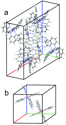 | ||
| Fig. 1 Unit cells with complete molecules of (a) Zn(BQA)2 obtained from sublimation and (b) Fe(BQA)2 crystallized from solution. | ||
In contrast, the intended stacking motif can be observed for Cr(BQA)2 (Fig. S24, ESI†) and Fe(BQA)2 (Fig. 1b). For Fe(BQA)2, in addition to a face-to-edge orientation, ligand planes are parallel displaced and face-to-face in the orthogonal direction, packing in a triclinic cell of a = 11.858 Å, b = 12.237 Å, c = 12.268 Å and α = 90.362°, β = 101.553°, γ = 116.949° within the P![[1 with combining macron]](https://www.rsc.org/images/entities/char_0031_0304.gif) space group. Interaction between ligands leaves free volume that is filled by solvent. Such π-stacking typically leads to strong electronic coupling.10 A similar structure was found for Cr(BQA)2 (Fig. S24, ESI†), with a corresponding triclinic unit cell of a = 9.072 Å, b = 12.758 Å, c = 16.071 Å, and α = 81.026°, β = 75.685°, γ = 79.295° within the P
space group. Interaction between ligands leaves free volume that is filled by solvent. Such π-stacking typically leads to strong electronic coupling.10 A similar structure was found for Cr(BQA)2 (Fig. S24, ESI†), with a corresponding triclinic unit cell of a = 9.072 Å, b = 12.758 Å, c = 16.071 Å, and α = 81.026°, β = 75.685°, γ = 79.295° within the P![[1 with combining macron]](https://www.rsc.org/images/entities/char_0031_0304.gif) space group. In an oxidized sample, aside from the solvent molecules, chloride ions were found characterizing the sample as [Cr(BQA)2]Cl (Fig. S25, ESI†) with a triclinic unit cell of a = 10.774 Å, b = 11.688 Å, c = 15.329 Å, α = 80.557°, β = 78.385°, γ = 68.265° within the P
space group. In an oxidized sample, aside from the solvent molecules, chloride ions were found characterizing the sample as [Cr(BQA)2]Cl (Fig. S25, ESI†) with a triclinic unit cell of a = 10.774 Å, b = 11.688 Å, c = 15.329 Å, α = 80.557°, β = 78.385°, γ = 68.265° within the P![[1 with combining macron]](https://www.rsc.org/images/entities/char_0031_0304.gif) space group. Partial oxidation of the synthesized Cr(BQA)2 is revealed but complete oxidation is excluded based on the UV/Vis spectra of the synthesized Cr(BQA)2 in comparison to [Cr(BQA)2]Cl (Fig. S3, ESI†). Clear differences in the spectral shape prove that the Cr(II) complex was synthesized, however, with potential contamination by Cr(III).
space group. Partial oxidation of the synthesized Cr(BQA)2 is revealed but complete oxidation is excluded based on the UV/Vis spectra of the synthesized Cr(BQA)2 in comparison to [Cr(BQA)2]Cl (Fig. S3, ESI†). Clear differences in the spectral shape prove that the Cr(II) complex was synthesized, however, with potential contamination by Cr(III).
Despite the use of identical ligands prior to complexation, quite different packing motifs emerge, depending on the central metal. The metal is coordinated by two ligands, with all nitrogen atoms forming ligand–metal bonds, resulting in a partially distorted octahedral coordination sphere. Both quinolinyl moieties within a given ligand are not perfectly coplanar because of the repulsive interaction of the hydrogen atoms at the positions 2 and 2′ of each moiety. In extension, the sizes of the metal centres, which can be compared by measuring the length of the six metal–nitrogen bonds, are reflected in the dihedral angles between the two quinolinyl moieties of each ligand. The size of the metal centre is defined by the number of d-electrons and the spin state of the complex. These geometric features were also investigated using DFT computations, which allows us to determine the spin states of the complexes.
The experimental crystal structures are not completely symmetric regarding individual ligands and corresponding bonds due to packing effects. In contrast, the computed individual metal complexes are completely symmetric. Still, the average bond lengths (Table S3, ESI†) and resulting dihedral angles within the crystal structure and the computations compare rather well, e.g., for Zn(BQA)2 (found 23.7°, calc.: 25.4°). The large angles found are in line with the large size of zinc(II) with its completely filled d-orbitals. The largest angle is measured for Mn(BQA)2 (found 25.8°, calc.: 28.9° for the sextet, 16.8° for the quartet state) suggesting the presence of a d5 high spin system. The iron(II) centre of Fe(BQA)2 (found 5.2°, calc.: 9.7°) is compact in size, as rationalized by a computed favoured d6 low spin state. For Cr(BQA)2, the two ligands showed differing dihedral angles of 7.9° and 19.0° (average of 13.5°) which also compares favourably with a calculated value of 15.7°. In general, more defined π–π stacking was found for smaller dihedral angles within this study, pointing at this angle as a good indicator for the overlap of the ligands’ π-orbitals. Variation of the central metal, therefore, leads to changes in molecular arrangement of the ligand in the complex as seen in the single crystal structure. Therefore, a strong influence of the different metal atoms on the molecular properties is expected.
Redox potentials of the first oxidation (Eox) and the first reduction (Ered) were obtained by CV in solution (Table 1, Fig. 2 and Fig. S2, ESI†). For Zn(BQA)2, the reduction could not be observed because of limitation by the potential window of the electrolyte solution. Eox of Zn(BQA)2 at 0.37 V vs. Ag/AgCl corresponds to a HOMO energy of −4.68 eV if calibrated against an external Fc/Fc+ couple. The potential is significantly lower than Eox reported for the ligand, which, by similar reference to Fc/Fc+, converts to a HOMO energy of −5.36 eV.20 Such a low Eox of Zn(BQA)2 emphasizes strong contributions of the metal centre. For the early transition metal complexes (Cr(BQA)2, Mn(BQA)2, and Fe(BQA)2), the values of Eox are also below that of the pure ligand, demonstrating that the HOMO includes contributions of metal orbitals to a significant proportion also in these cases. In extension, we observed a trend of easier oxidation with higher nuclear charge of the central metal. Both Mn(BQA)2 and Fe(BQA)2 are similar in their redox properties, showing reversible oxidation and reduction at almost the same potential, which is explained by their direct neighbourhood in the periodic table of the elements. Two oxidation waves were observed for Cr(BQA)2, which is typical for chromium complexes that often display a broad range of oxidation states.32 Cr(BQA)2 is reduced in an irreversible wave at significantly lower Ered.
| E ox (V) | E HOMO (−eV) | E red (−V) | E LUMO (–eV) | E gap (eV) | Optical gap (eV) | |
|---|---|---|---|---|---|---|
| Zn(BQA)2 | 0.37 | 4.68 | — | — | — | 2.25 |
| Cr(BQA)2 | 0.87 | 5.18 | 1.07 | 3.24 | 1.94 | 2.02 |
| Mn(BQA)2 | 0.75 | 5.06 | 0.24 | 4.07 | 0.99 | 2.12 |
| Fe(BQA)2 | 0.62 | 4.93 | 0.34 | 3.97 | 0.96 | 1.45 |
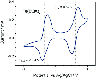 | ||
| Fig. 2 Cyclic voltammogram of Fe(BQA)2 dissolved in DMF. Dashed lines indicate the redox potentials Ered and Eox. | ||
The measured UV/Vis absorbance spectra also clearly reflect the influence of the central metal on the electronic structure of the complexes and correspond to literature data: below an upper limit of around 600 nm bands are commonly assigned to ligand centered π–π* transitions, while at higher wavelengths d-orbital transitions become prevalent.18,20,33 Results obtained for Zn(BQA)2 in comparison to BQAH are shown in Fig. 3a. The ligand has a well-defined absorption band at 400 nm, which is shifted to higher wavelength (500 nm) in Zn(BQA)2 caused by coordination to the metal centre. Above 575 nm, no transitions are found, since all d-orbitals are occupied.
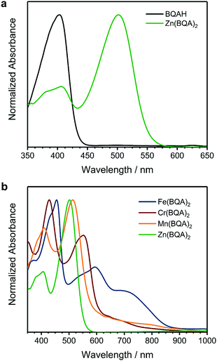 | ||
| Fig. 3 UV/Vis absorption spectra in DMF solution of (a) BQAH and Zn(BQA)2 and (b) of all complexes in direct comparison. | ||
Mn(BQA)2 showed very similar spectral features below 600 nm (Fig. 3b), which are assigned to ligand-centred transitions. This is supported by only small differences in the dihedral angle of the ligand. Consequently, just a small red-shift was observed relative to Zn(BQA)2. Furthermore, we observed a range of weak transitions from 600–900 nm, which can be assigned to the (albeit unfavourable because spin-forbidden) d-orbital transitions in the high spin complex. The optical gap (Table 1) is substantially larger than the difference between Ered and Eox, indicating the presence of states that cannot be accessed by photon excitation below the S0–S1 transition. The spectrum measured for Cr(BQA)2 was very similar to that of Mn(BQA)2, with the two high energy bands and a weaker transition at higher wavelength. In the high energy range, the spectral shape is influenced by a lower dihedral angle of the ligand. The optical gap of Cr(BQA)2 fits well to EGap found by CV, demonstrating the optical transition to be equivalent within good approximation. In line with previous findings, the spectrum of the presumably low spin Fe(BQA)2 complex (see calculated results in Fig. S1, ESI†) showed significantly stronger absorptions above 600 nm. Below 600 nm, ligand-centred transitions are influenced substantially by the significantly lower dihedral angle. The red-shift of the ligand-centred bands (Fe(BQA)2 > Cr(BQA)2 > Mn(BQA)2 ≈ Zn(BQA)2) inversely correlates with the dihedral angle between the quinolinyl moieties (Fe(BQA)2 < Cr(BQA)2 < Mn(BQA)2 ≈ Zn(BQA)2). A higher planarity (lower dihedral angle) in the BQA ligand obviously leads to increased orbital delocalization and, hence, decreased transition energy.
Thin films were prepared by PVD at temperatures of Fe(BQA)2 (129 ± 22 °C) ≈ Cr(BQA)2 (129 ± 12 °C) > Mn(BQA)2 (120 ± 8 °C) > Zn(BQA)2 (104 ± 12 °C), indicating stronger intermolecular coupling and higher lattice energy for complexes with a smaller dihedral angle. All complexes could be evaporated and resublimed without decomposition. This is most clearly seen for Zn(BQA)2 since vapour-grown single crystals could be obtained (Fig. 1a). The stability of Zn(BQA)2 and Fe(BQA)2 during thin film preparation was confirmed by ESI-MS analysis of the source materials compared to vapour-deposited thin film samples (Fig. S4 and S5, ESI†), in which no significant impurities were observed. Integrity of the metal complexes upon the deposition of thin films is also seen in quite similar band positions of the chromophores in optical absorption spectra of the thin films compared to solutions (Fig. 4 exemplarily shows this for Fe(BQA)2, see Fig. S6 for others, ESI†).
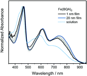 | ||
| Fig. 4 Thickness dependent UV-vis absorbance of Fe(BQA)2 subsequently measured during PVD onto quartz glass. The solution spectrum (from Fig. 3b) is provided as dotted line for direct comparison. | ||
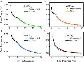
Detailed inspection reveals that the absorption band positions for thin films of all complexes except Cr(BQA)2 are shifted towards lower energy when compared to spectra in solution. Such a shift is typically caused by changes in the dielectric environment (organic solid vs. solution). For increasingly thicker films, the optical absorbance maximum showed a red-shift (Fig. 4 and Fig. S6, ESI†). In the monolayer regime (around 1 nm), isolated molecules interact with the substrate, while increasing coverage leads to intermolecular coupling, which ultimately decreases the energy of the band towards its bulk value.34 Such intermolecular coupling of frontier orbitals is of significance for charge transport since these energy levels host the conducting electrons or holes. For Zn(BQA)2, Mn(BQA)2, and Cr(BQA)2 frontier orbital transitions were mainly ligand-centred. Taking the shift of the peak around 550 nm from 1 to 20 nm film thickness as an estimate for the difference between isolated and bulk energy (Fig. 5), values of 50 meV for Zn(BQA)2 (516–527 nm) and Mn(BQA)2 (528–540 nm) were obtained. The shift for Cr(BQA)2 (512–535 nm) was found significantly larger (100 meV), in line with the increased π–π stacking of ligands in the crystal lattice. The frontier orbital transition in Fe(BQA)2 was found at a notably higher wavelength and still yields a 40 meV (722–740 nm) shift, despite the fact that it corresponds to a metal-centred transition.
Thickness-dependent shifts of the absorption bands can, further, indicate changes in the growth-mode of organic materials. For layered growth, the peak energy of an absorption band can be expressed as a function of thickness d:
| E(d) = Ebulk + ΔE × dint/d |
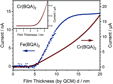
Regarding the data shown in Fig. 5, two regimes were identified in the decrease of the band energies for Zn(BQA)2, Mn(BQA)2, and Fe(BQA)2: one up to about d = 5 nm characteristic for a decreasing influence of isolated molecules and one above d = 5 nm characteristic for a decreasing ratio of surface to bulk molecules. The data were fitted according to 1/d. In case of Fe(BQA)2 (Fig. 5c), this transition at d = 5 nm correlates well with the beginning of measurable current between interdigitated electrodes, when the current is monitored depending on film thickness (Fig. 6). Up to 5 nm film thickness, growth of isolated islands seems to be the preferred growth mode for Fe(BQA)2. The surface to molecule interaction should contribute in such thin films, as seen by the strong decrease of band energy. Independent atomic force microscopy (AFM) studies confirmed these islands (Fig. S7a, ESI†). At the onset of a linear increase in current (Fig. 6), percolation leads to the closing of gaps between islands (Fig. S7b, ESI†). The linear increase with film thickness up to 12 nm corresponds to the filling of these gaps (Fig. S7c, ESI†), after which the current remains almost constant. Therefore, further island growth on top of the film occurred, which had little influence on the optical shift. The second regime in Fig. 5c, corresponding suitably well to the 1/d relationship, is assigned to an increased relevance of the bulk energy. Similar behaviour was found when investigating the shift for Zn(BQA)2 and Mn(BQA)2 (Fig. 5a and b), both displaying the plateau at 5 nm or 4 nm, respectively, in an even more pronounced way, proving a similar growth mode as for Fe(BQA)2. In case of Cr(BQA)2, conductive pathways form already at 2.1 nm film thickness, significantly closer to the monolayer regime (inset Fig. 6). Islands start to be in contact at lower film thickness and the plateau in the decrease of band energy to the bulk value is masked (Fig. 5d). The absence of any plateau in the current dependent on thickness (Fig. 6) indicates monotonous growth of Cr(BQA)2 thin films.
A first outlook on the electrical performance of the investigated complexes to discuss their suitability as organic semiconductors can be gained from thin films in a bottom gate bottom contact field-effect transistor geometry. A silicon wafer with thermally grown oxide as a gate insulator and two interdigitated Au electrodes was chosen because of its simple device architecture (Fig. S11, ESI†). The Au electrode work function of 4.7 eV, determined by Kelvin probe force microscopy, when compared to the determined HOMO energies, should provide Ohmic contact characteristics to the studied films. This is confirmed by a pronounced linear regime in the transfer characteristics (insets of Fig. 7, details in Fig. S12, ESI†).36
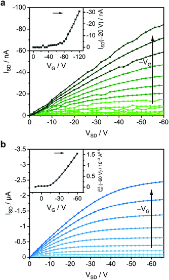 | ||
| Fig. 7 OFET output characteristics of (a) an 88 nm thin film of Zn(BQA)2 and (b) a thin film of Fe(BQA)2 with their transfer curves as insets (details in Fig. S12, ESI†). For Zn(BQA)2, the transfer curve is evaluated in the linear regime since Zn(BQA)2 devices lack saturation. | ||
Conductivities and charge carrier mobilities were measured and show significant differences for the four studied materials. Such differences can be of intrinsic character and originate from different intermolecular coupling within grains of the films or can originate from different transport across grain boundaries caused by variations of film morphology. In a first approximation, a significant influence of film morphology is excluded since identical growth modes of the four materials were observed by shifts of the absorption energies (Fig. 5) and since AFM studies for Zn(BQA)2 and Fe(BQA)2 on the OFET substrates verified a similar morphology (Fig. S8, ESI†).
Output characteristics representative for Zn(BQA)2 thin films are shown in Fig. 7a. Negative gate voltages increase the current as also seen in the transfer curves (inset of Fig. 7a and details in Fig. S12, ESI†), which identifies Zn(BQA)2 as p-type semiconductor. The currents observed are in the 0–100 nA range. A conductivity of less than 1.9 × 10⁻⁹ S m−1 (instrumentational limit) can be estimated at VG = 0 V and a charge carrier mobility of μ(−20 V) = 9.5 × 10⁻⁷ cm2 V−1 s−1 was determined, both rather low compared to many other organic semiconductors.1,37 Accordingly, a small on/off-ratio of about 15 was determined for ISD at maximum VG compared to VG = 0 V. The threshold voltage Vth = −74.0 V (Fig. S12, ESI†) indicates significant hole trapping at the SiO2/Zn(BQA)2 interface.
Thin films of Fe(BQA)2 (Fig. 7b and Fig. S12, ESI†) also showed p-type characteristics with, however, a significantly higher charge carrier mobility of μ(−60 V) = 8.1 × 10⁻⁵ cm2 V−1 s−1. This higher mobility is similar to that of, e.g., iron(II) phthalocyanine, an established iron(II) complex as organic semiconductor, measured in a similar device setup.38 The On/Off ratio of Fe(BQA)2 was determined as 1178. A threshold voltage Vth = −18.7 V again points at hole-trapping at the interface to SiO2.
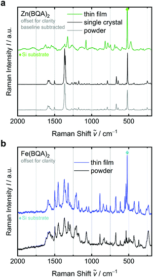
Such improved performance of Fe(BQA)2 thin films compared to those of Zn(BQA)2 comes in line with the well-ordered face-to-face and parallel displaced π–π stacking found for single crystals of Fe(BQA)2 (Fig. 1) as opposed to those of Zn(BQA)2, for which such well-defined and constant relative arrangement of the ligands was not seen. Electric characteristics of the thin films, therefore, appear reasonable in view of different solid-state packing structures observed in the single crystals. Thin films of organic semiconductors, however, can show a structure different from that of single crystals and, therefore, the structure of the thin films deserves further attention. The crystal structures of powder samples were independently shown to be compatible to the single crystal structures by X-ray powder diffraction (Fig. S9 and S10, ESI†). To discuss the significance of such stacking patterns in the thin films, Raman spectroscopy on films, source materials and a single crystal was performed (Fig. 8). Raman scattering is very sensitive to structural changes. For Zn(BQA)2, the Raman spectrum of a sublimation-grown single crystal was identical to that of the powder source material (Fig. 8a). In contrast, however, the spectrum of a Zn(BQA)2 thin film differs significantly from those of crystal and powder. Since the molecular structure is unchanged during PVD of the thin films (Fig. S4, ESI†), differences are revealed in the molecular packing within Zn(BQA)2 thin films vs. powder or single crystal. For Fe(BQA)2, however, widely identical Raman band positions and intensity ratios were obtained for thin film and powder samples (Fig. 8b), proving the intended transfer of the well-ordered stacking motif (Fig. 1b) to thin film devices. The planarity and small dihedral angle in Fe(BQA)2 leads to well-defined π–π interaction. Such stacking motif proved to be more stable and was transferred into working OFET devices with reasonable charge carrier mobility. For distorted ligands as in Zn(BQA)2, a less defined molecular arrangement was obtained in vapour-deposited thin films, characteristic for weakly interacting complexes.
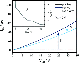
Venting the chamber with air after film preparation of Fe(BQA)2 and initial OFET measurements leads to an increase in current (Fig. 9 and Fig. S13, ESI†), corresponding to an increase of the hole concentration indicating partial oxidation by O2. The conductivity changes by several orders of magnitude from 9.9 × 10⁻⁹ S m−1 to 1.6 × 10⁻³ S m−1. Caused by such high concentration of charge carriers, VG has only little influence on ISD in this state (Fig. S13, ESI†). To avoid partial oxidation of the material already before film preparation, the evaporation source for the majority of experiments was sealed by a gate valve and the source was filled under inert gas in a glove box. Devices fabricated without such precautions showed a decreased on/off ratio of only 80 (Fig. S14, ESI†) caused by an increased hole concentration as a consequence of partial oxidation, but the charge carrier mobility was widely preserved at μ(−50 V) = 7.5 × 10⁻⁵ cm2 V−1 s−1, indicating unchanged film growth. Deliberate subsequent exposure to air also of such films led to an increase of the conductivity from 7.7 × 10⁻⁸ S m−1 to 5.4 × 10⁻⁴ S m−1. Restoring high vacuum partly reversed the oxidation over the course of two days (Fig. 9). Such interaction with air was only observed for Fe(BQA)2 but not for Zn(BQA)2 despite its lower Eox, which must be due to the singlet spin state of the Zn-complex kinetically hindering the oxidation by triplet O2.
No current above the detection limit was measured for Mn(BQA)2 thin films, independent of the applied gate voltage. Interaction with air also did not give rise to a measurable current. We assume that this is due to a low charge carrier mobility, a hypothesis supported by the low degree of π–π-stacking found in Mn(BQA)2 single crystals. Based on the estimated HOMO energy, injection of charge carriers from Au should be feasible and film growth similar to the other complexes was observed (Fig. 5), so that a compact layer of molecules can be expected. Cr(BQA)2 thin films showed a high conductivity of 0.33 S m−1, extracted from a linear fit of the current voltage plot at high voltage (Fig. S15, ESI†) directly after deposition, i.e., in high vacuum, indicating a high charge carrier concentration, since no field-effect was observed. As is the case for Fe(BQA)2, ligands in the single crystal structure showed clear π-system interaction, suggesting facile charge carrier transport. As-deposited Cr(BQA)2 thin films already contained chromium(III) leading to p-doping of the film, since partial oxidation during synthesis was seen in the UV-Vis absorbance spectra (Fig. S3, ESI†). Exposing such films to air leads to an irreversible oxidation and loss of conductivity (Fig. S15, ESI†). Changes in the absorbance spectra of the thin films (Fig. S3, ESI†) showed such oxidation of the complex, when compared to Cr(BQA)2 and [Cr(BQA)2]Cl in solution. Consequently, the as-deposited hole-conducting films become insulating following complete oxidation by air.
Conclusions
The targeted neutral complexes were synthesized and their structures were determined by single crystal X-ray diffraction. The expected π–π stacking in two orthogonal directions was discerned for Fe(BQA)2 and Cr(BQA)2 in the crystal structures as opposed to Zn(BQA)2 and Mn(BQA)2 with a variety of ligand-to-ligand orientations. The different central metals showed a clear influence on the dihedral angle of the ligands, correlating to metal centre size, which directly led to significantly different relative orientation of the ligands and, hence, different crystal structures. A corresponding trend in HOMO energies was found by CV. For the most part, reversible oxidation and reduction waves were observed, with the exception of Cr(BQA)2. Furthermore, UV/Vis absorption of the complexes differs depending on the d-orbital configuration of the central metal. Bands at higher wavelengths were observed in particular for Fe(BQA)2.The complexes were sublimed and deposited without decomposition and thin films were prepared by PVD. Absorption bands were found progressively red-shifted with increasing film thickness. Comparing these shifts to thickness-dependent AFM measurements, as well as to the development of electric current along growing films, a constant growth mode was observed for the different metal complexes. On micro-structured interdigitated Au electrode arrays, thin films of Zn(BQA)2 were characterized as p-doped with low conductivity and charge carrier mobility of (8.9 ± 0.7) × 10−7 cm2 V−1 s−1, consistent with a low degree of π–π stacking of distorted complexes. Mn(BQA)2 does not conduct significantly, while Cr(BQA)2 on the other hand is strongly conductive at 0.33 S m−1, caused by partial oxidation. For Fe(BQA)2, we obtained p-type conduction and a field-effect mobility of (5.6 ± 3.1) × 10−5 cm2 V−1 s−1 depending on environmental conditions, but substantially higher than the values for Zn(BQA)2, consistent with a considerably more efficient π–π stacking of planar ligands. Significant differences in redox behaviour upon exposure to air were found for the films. Zn(BQA)2 devices are air-stable. Exposing Cr(BQA)2 films to air leads to a complete loss of its initially high conductivity. The partially reversible response of Fe(BQA)2 to oxygen from air indicates some potential as a chemical sensor.
We demonstrated that the structures of BQA complexes are strongly influenced by different central metals, which has significant consequences for their molecular properties. Thin films of complexes which showed the intended face-to-face and face-to-edge type π–π stacking (e.g. Fe(BQA)2) showed higher conductivity and charge carrier mobility than those, which did not show such high order in thin films and just showed face-to-edge type stacking with no constant relative orientation even in single crystals (e.g. Zn(BQA)2). This conclusion of an influence of molecular packing is valid even if a superimposed influence of transport properties across grain boundaries at present cannot be fully excluded despite quite similar growth characteristics and morphologies of the films grown from the different complexes. The electrical performance of the materials as of yet is not on par with high mobility materials. This may at least in part be caused by a residual influence of grain boundaries, which is indicated by the observed island growth and which often can be cured by interface modification and fine-tuning of the deposition conditions.
In fulfilment of the outlined strategy, we established the intended π–π stacking motif for thin film devices of Fe(BQA)2, essential for their electrical performance. In analogy to atoms in inorganic semiconductors, the complexes should be interchangeable to a certain extent because of closely related size and structure. Charged complexes obtained by oxidation of one central metal (e.g., Cr) can then be used as dopants in pristine films of the same ligand's complex with another central metal (e.g., Fe). Chemical substitution at the ligand π-system offers means to modify its structure and energy level position as recently shown, e.g., for Fe(phenanthridin-4-yl)(quinolin-8-yl)amido-complexes.39 Similar modification at the BQA ligand aims at improved intermolecular electronic coupling, stabilisation of the targeted stacking motif and, thereby, improved electrical characteristics of the solids. Such studies are presently ongoing in our laboratories as well as detailed characterization of contact formation with other semiconductors or metals.
Conflicts of interest
There are no conflicts of interest to declare.Acknowledgements
Financial support was provided by the DFG via the GRK (Research Training Group) 2204 “Substitute Materials for Sustainable Energy Technologies”. We are very grateful to F. Willming (Inst. of Organic Chemistry, JLU), C. Geis (Inst. of Applied Physics, JLU), and to P. Cop (Inst. of Physical Chemistry, JLU) for their valuable support in ESI-MS, AFM, and powder XRD measurements, respectively.References
- A. K. Asatkar, A. Bedi and S. S. Zade, Metallo-organic conjugated systems for organic electronics, Isr. J. Chem., 2014, 54, 467–495 CrossRef CAS
.
- A. K. Asatkar, S. P. Senanayak, A. Bedi, S. Panda, K. S. Narayan and S. S. Zade, Zn(II) and Cu(II) complexes of a new thiophene-based salphen-type ligand: Solution-processable high-performance field-effect transistor materials, Chem. Commun., 2014, 50, 7036–7039 RSC
.
- T. Taguchi, H. Wada, T. Kambayashi, B. Noda, M. Goto, T. Mori, K. Ishikawa and H. Takezoe, Comparison of p-type and n-type organic field-effect transistors using nickel coordination compounds, Chem. Phys. Lett., 2006, 421, 395–398 CrossRef CAS
.
- L. Li, Q. Tang, H. Li, W. Hu, X. Yang, Z. Shuai, Y. Liu and D. Zhu, Organic thin-film transistors of phthalocyanines, Pure Appl. Chem., 2008, 80, 2231–2240 CAS
.
- A. S. Başak, A. R. Ozkaya, A. Altındal, B. Salih, A. Sengül and O. Bekaroğlu, Synthesis, characterization, oxygen electrocatalysis and OFET properties of novel mono- and ball-type metallophthalocyanines, Dalton Trans., 2014, 43, 5858–5870 RSC
.
- M. Hanack and M. Lang, Conducting stacked Metallophthalocyanines and related compounds, Adv. Mater., 1994, 6, 819–833 CrossRef CAS
.
- C. Wang, H. Dong, W. Hu, Y. Liu and D. Zhu, Semiconducting π-conjugated systems in field-effect transistors: A material odyssey of organic electronics, Chem. Rev., 2012, 112, 2208–2267 CrossRef CAS PubMed
.
- Y. Miyake, Y. Shiraiwa, K. Okada, H. Monobe, T. Hori, N. Yamasaki, H. Yoshida, M. J. Cook, A. Fujii, M. Ozaki and Y. Shimizu, High carrier mobility up to 1.4 cm2 V−1 s−1 in non-peripheral octahexyl phthalocyanine, Appl. Phys. Exp., 2011, 4, 21604 CrossRef
.
- H. Wang, D. Song, J. Yang, B. Yu, Y. Geng and D. Yan, High mobility vanadyl-phthalocyanine polycrystalline films for organic field-effect transistors, Appl. Phys. Lett., 2007, 90, 253510 CrossRef
.
- Z.-F. Yao, J.-Y. Wang and J. Pei, Control of π–π stacking via crystal engineering in organic conjugated small molecule crystals, Cryst. Growth Des., 2017, 18, 7–15 CrossRef
.
- R. D. Gould, Structure and electrical conduction properties of phthalocyanine thin films, Coord. Chem. Rev., 1996, 156, 237–274 CrossRef CAS
.
- Z. A. Lamport, H. F. Haneef, S. Anand, M. Waldrip and O. D. Jurchescu, Tutorial: Organic field-effect transistors: Materials, structure and operation, J. Appl. Phys., 2018, 124, 71101 CrossRef
.
- K. Ito, T. Suzuki, Y. Sakamoto, D. Kubota, Y. Inoue, F. Sato and S. Tokito, Oligo(2,6-anthrylene)s, Angew. Chem., Int. Ed., 2003, 42, 1159–1162 CrossRef CAS PubMed
.
- J. Clark, C. Silva, R. H. Friend and F. C. Spano, Role of intermolecular coupling in the photophysics of disordered organic semiconductors, Phys. Rev. Lett., 2007, 98, 206406 CrossRef PubMed
.
- K. Xiao, Y. Liu, T. Qi, W. Zhang, F. Wang, J. Gao, W. Qiu, Y. Ma, G. Cui, S. Chen, X. Zhan, G. Yu, J. Qin, W. Hu and D. Zhu, A highly pi-stacked organic semiconductor for field-effect transistors based on linearly condensed pentathienoacene, J. Am. Chem. Soc., 2005, 127, 13281–13286 CrossRef CAS PubMed
.
- X. Yang, L. Wang, C. Wang, W. Long and Z. Shuai, Influences of crystal structures and molecular sizes on the charge mobility of organic semiconductors, Chem. Mater., 2008, 20, 3205–3211 CrossRef CAS
.
- G. Kinunda and D. Jaganyi, Understanding the electronic and π-conjugation roles of quinoline on ligand substitution reactions of platinum(II) complexes, Transition Met. Chem., 2014, 39, 451–459 CrossRef CAS
.
- D. Maiti, H. Paul, N. Chanda, S. Chakraborty, B. Mondal, V. G. Puranik and G. K. Lahiri, Synthesis, structure, spectral and electron-transfer properties of octahedral-[CoIII(L)2]+/[ZnII(L)2] and square planar-[CuII(L){OC(
![[double bond, length as m-dash]](https://www.rsc.org/images/entities/char_e001.gif) O)CH3}] complexes incorporating anionic form of tridentate bis(8-quinolinyl)amine [N1C9H6–N2–C9H6N3, L−] ligand, Polyhedron, 2004, 23, 831–840 CrossRef CAS
O)CH3}] complexes incorporating anionic form of tridentate bis(8-quinolinyl)amine [N1C9H6–N2–C9H6N3, L−] ligand, Polyhedron, 2004, 23, 831–840 CrossRef CAS .
- P. Mandapati, P. K. Giesbrecht, R. L. Davis and D. E. Herbert, Phenanthridine-containing pincer-like amido complexes of nickel, palladium, and platinum, Inorg. Chem., 2017, 56, 3674–3685 CrossRef CAS PubMed
.
- T. A. Betley, B. A. Qian and J. C. Peters, Group VIII coordination chemistry of a pincer-type bis(8-quinolinyl)amido ligand, Inorg. Chem., 2008, 47, 11570–11582 CrossRef CAS PubMed
.
- L. Canovese, F. Visentin, G. Chessa, C. Levi and P. Nikolov, Luminescent complexes of the zinc triad with N-substituted 8-amino-quinoline ligands: Synthesis and comparative study on the stability constants and related photophysical properties, Inorg. Chim. Acta, 2009, 362, 3925–3933 CrossRef CAS
.
- K. H. Wedepohl, The composition of the continental crust, Geochim. Cosmochim. Acta, 1995, 59, 1217–1232 CrossRef CAS
.
- A. M. Whyte, B. Roach, D. K. Henderson, P. A. Tasker, M. M. Matsushita, K. Awaga, F. J. White, P. Richardson and N. Robertson, Structural, magnetic, and electronic properties of phenolic oxime complexes of Cu and Ni, Inorg. Chem., 2011, 50, 12867–12876 CrossRef CAS PubMed
.
- J. P. Perdew, K. Burke and M. Ernzerhof, Generalized gradient approximation made simple, Phys. Rev. Lett., 1996, 77, 3865–3868 CrossRef CAS PubMed
.
- J. P. Perdew, K. Burke and M. Ernzerhof, Generalized gradient approximation made simple [Phys. Rev. Lett. 77, 3865 (1996)], Phys. Rev. Lett., 1997, 78, 1396 CrossRef CAS
.
- F. Weigend and R. Ahlrichs, Balanced basis sets of split valence, triple zeta valence and quadruple zeta valence quality for H to Rn, Phys. Chem. Chem. Phys., 2005, 7, 3297–3305 RSC
.
- F. Weigend, Accurate Coulomb-fitting basis sets for H to Rn, Phys. Chem. Chem. Phys., 2006, 8, 1057–1065 RSC
.
- I. M. Dixon, S. Khan, F. Alary, M. Boggio-Pasqua and J.-L. Heully, Probing the photophysical capability of mono and bis(cyclometallated) Fe(II) polypyridine complexes using inexpensive ground state DFT, Dalton Trans., 2014, 43, 15898–15905 RSC
.
- Cambridge Crystallographic Data Centre, Cambridge Structural Database, https://www.ccdc.cam.ac.uk/structures/, (accessed January 2021).
- J. Pommerehne, H. Vestweber, W. Guss, R. F. Mahrt, H. Bässler, M. Porsch and J. Daub, Efficient two layer leds on a polymer blend basis, Adv. Mater., 1995, 7, 551–554 CrossRef CAS
.
- J. C. S. Costa, R. J. S. Taveira, C. F. R. A. C. Lima, A. Mendes and L. M. N. B. F. Santos, Optical band gaps of organic semiconductor materials, Opt. Mater., 2016, 58, 51–60 CrossRef CAS
.
- H. H. Downs, R. M. Buchanan and C. G. Pierpont, Multistep redox series of the tris(o-semiquinone)chromium(III) complexes, Inorg. Chem., 1979, 18, 1736–1740 CrossRef CAS
.
-
A. B. P. Lever, Inorganic Electronic Spectroscopy, Elsevier Science, Amsterdam, Oxford, New York, Tokio, 1984 Search PubMed
.
- I. Trenkmann, C. von Borczyskowski and H. Graaf, Shift of absorption energy during thin dye film growth, Thin Solid Films, 2014, 573, 41–47 CrossRef CAS
.
- U. Heinemeyer, K. Broch, A. Hinderhofer, M. Kytka, R. Scholz, A. Gerlach and F. Schreiber, Real-time changes in the optical spectrum of organic semiconducting films and their thickness regimes during growth, Phys. Rev. Lett., 2010, 104, 257401 CrossRef CAS PubMed
.
- C. Liu, G. Li, R. Di Pietro, J. Huang, Y.-Y. Noh, X. Liu and T. Minari, Device physics of contact issues for the overestimation and underestimation of carrier mobility in field-effect transistors, Phys. Rev. Appl., 2017, 8, 034020 CrossRef
.
- S. R. Forrest, The path to ubiquitous and low-cost organic electronic appliances on plastic, Nature, 2004, 428, 911–918 CrossRef CAS PubMed
.
- Z. Bao, A. J. Lovinger and A. Dodabalapur, Highly ordered vacuum-deposited thin films of metallophthalocyanines and their applications in field-effect transistors, Adv. Mater., 1997, 9, 42–44 CrossRef CAS
.
- J. D. Braun, I. B. Lozada, C. Kolodziej, C. Burda, K. M. E. Newman, J. van Lierop, R. L. Davis and D. E. Herbert, Iron(II) coordination complexes with panchromatic absorption and nanosecond charge-transfer excited state lifetimes, Nat. Chem., 2019, 11, 1144–1150 CrossRef CAS PubMed
.
Footnotes |
| † Electronic supplementary information (ESI) available. CCDC 1897889–1897893 and 2057276. For ESI and crystallographic data in CIF or other electronic format see DOI: 10.1039/d1ma00078k |
| ‡ These authors contributed equally. |
| This journal is © The Royal Society of Chemistry 2021 |


