
 Open Access Article
 This Open Access Article is licensed under a Creative Commons Attribution-Non Commercial 3.0 Unported Licence
Out of stoichiometry CuCrO2 films as a promising p-type TCO for transparent electronics†
Lorenzo
Bottiglieri
 *a,
João
Resende
b,
Matthieu
Weber
a,
Odette
Chaix-Pluchery
a,
Carmen
Jiménez
a and
Jean-Luc
Deschanvres
a
*a,
João
Resende
b,
Matthieu
Weber
a,
Odette
Chaix-Pluchery
a,
Carmen
Jiménez
a and
Jean-Luc
Deschanvres
a
aUniv. Grenoble Alpes, CNRS, Grenoble INP, LMGP, F-38000 Grenoble, France. E-mail: Lorenzo.bottiglieri@grenoble-inp.fr; Jean-luc.deschanvres@grenoble-inp.fr
bAlmaScience, Campus da Caparica, 2829-516 Caparica, Portugal
First published on 3rd June 2021
Abstract
In this work, we report the enhancement of the functional properties of CuCrO2, a promising p-type transparent conductive oxide, achieved in out of stoichiometry CuCrO2 thin films synthesized by aerosol-assisted chemical vapor deposition. Out of stoichiometry films consisting of Cr-deficient CuCrO2, i.e. Cu-rich CuCrO2 phase, have a resistivity value of 0.05 Ω cm and an average transmittance of 58% in the visible range, resulting in a Gordon's figure of merit of 2200 μS. This is the highest ever published figure of merit among Cu-rich CuCrO2 films synthesized by chemical methods. A remarkable result is that when further increasing the Cu/(Cu + Cr) ratio, the formation of CuO was not detected, allowing the synthesis of composite films formed by Cu2O and CuCrO2 p-type oxides, which are more conductive than the Cu-rich CuCrO2 phase. These nanocomposite films present an improved carrier mobility, with a resistivity value of around 0.02 Ω cm, and a reduced energy gap, with a transmittance of 52%, resulting in a figure of merit of 1400 μS. Both these thin films can find applications as a hole transport layer in various transparent optoelectronic devices where p-type TCOs are required, especially when synthesized by a solution-based process at a low temperature and ambient pressure over large surface areas.
Introduction
Transparent electronics and the conception of see-through devices require materials combining high electrical conductivity and optical transmittance in the visible range, properties fulfilled by transparent conductive oxides (TCOs). The figure of merit as reported by Gordon1 (FoMG) can be used to quantify their performance. It is defined as the ratio of the electrical conductivity σ to the optical absorption α, resulting in: | (1) |
The massive breakthrough of transparent electronics is hindered by the lack of p-type TCOs with properties comparable to those of their n-type counterparts, the latter being characterized by an optical transmittance of around 80% in the visible range and a resistivity value as low as 0.001 Ω cm leading to a FoMG value of more than 200 mS.2 The development of p-type TCOs with high FoMG values allows the fabrication of fully transparent p–n junctions, as previously reported for Li-doped ZnO/ZnO,3 and Sb-doped p-type SnO2/Sb-doped n-type SnO2,3,4 although these devices were fabricated by physical deposition methods working at a high temperature.
In the hot topic of the synthesis of highly performing p-type TCOs, copper-based delafossite oxides with the general formula Cu1+M3+O2 (M = Al,5 Fe,6 Ge,7 Ga,8 Cr,9 Y10 or Sc11) arise as promising materials since the first report on CuAlO25 was characterized by p-type conductivity and good transparency. Among these, copper chromium oxide, CuCrO2, emerges as an ideal p-type TCO with a band gap of around 3.1–3.3 eV,12 ensuring good transparency and a relatively good electrical resistivity (ρ = 1 Ω cm) for stoichiometric films.13 These optical and electrical properties make it suitable for a wide variety of optoelectronic devices, such as photovoltaic devices,14,15 light16 and gas sensors,17 transparent diodes18 and transistors.19 Furthermore, this material is also attractive for other peculiar features such as its magnetic properties,20 photocatalytic ability,21 and thermoelectric properties.22 CuCrO2 films can be synthesized through different techniques such as sputtering,23 chemical vapour deposition (CVD),9,24 spray pyrolysis,25,26 atomic layer deposition (ALD),13 sol gel,27 hydro-thermal synthesis,28 molecular-beam epitaxy29 and pulsed laser deposition (PLD).30 Among them, chemical methods allow the deposition over large surface areas at a relatively low temperature (<400 °C), compatible with glass and even plastic substrates. These features are extremely appealing for industrial applications.
Concerning the transport mechanisms in CuCrO2, a small polaron hopping among Cu1+/Cu2+ sites12 was suggested as the conduction mechanism. Theoretical calculations12 showed that the p-type conductivity is related to the formation of defects, such as Cu vacancies (VCu), which have the lowest formation energy as confirmed by the experimental reports.24 Furthermore, various studies30,31 highlighted the possible formation of Cu anti-site defects (CuCr), i.e. Cu atoms occupying Cr sites. Intrinsic dopants are demonstrated to be responsible for the enhancement of the charge carrier density and, consequently, of the electrical properties. The kind of defects formed in the material is believed to be dependent on the growth conditions and finally on the deviation from the stoichiometry of CuCrO2.24–26,32 For instance, the high conductivity of Cu-deficient CuCrO2 films is attributed to the presence of Cu vacancies as detected by using scanning transmission electron microscopy (STEM).33
Several published studies concern the characterization of Cu-poor CuCrO2 films. Crêpellière et al.24 reported the synthesis by the pulsed-injection metal–organic CVD (PI-MOCVD) of films with a copper content Cu/(Cu + Cr) of 33%, still preserving the crystalline delafossite phase. These films presented a resistivity value of around 0.06 Ω cm and an average transmittance of around 50% in the visible range, yielding the highest FoMG value of 2300 μS, to date, for this material. Lunca Popa et al.33 reported the lowest resistivity value of 0.009 Ω cm achieved for the same Cu-poor composition, Cu0.66Cr1.33O2, synthesized by direct liquid injection MOCVD (DLI-MOCVD). Farrell et al.25 reported a slightly lower FoMG value of 350 μS for Cu-deficient CuCrO2 films with a Cu/(Cu + Cr) of ≈ 30–35% and oxygen in excess (Cu0.4CrO2.5) by using a non-vacuum technique, the spray pyrolysis. They reported a resistivity value of around 0.08 Ω cm and an average transmittance of 55%.
On the other hand, Cu-rich CuCrO2 films, i.e. Cr-poor CuCrO2 (CuCr1−xO2), have also been reported as a promising p-type TCO. Ling et al.34 reported the synthesis of CuCr1−xO2 by the solid-state reaction at a high temperature, showing a variation of the resistivity of two orders of magnitude for x = 0.1 compared to the stoichiometric sample.34 They attributed this enhancement to hybridization between Cu 3d and O 2p orbitals and the presence of a mixed-valence band Cu1+/Cu2+. Sidik et al.30 reported the synthesis of CuCr1−xO2 by PLD with a resistivity value of 0.04 Ω cm and an average optical transmittance of 60% for x = 0.03. The enhancement of the conductivity with Cr deficiency was linked to the presence of Cu atoms in Cr-vacancies to form Cu anti-site defects. Nevertheless, it was also reported that a high Cu content leads to the formation of a parasitic CuO24,27 phase, detrimental for the optoelectronic properties of the film.
To date, there is no report on the enhancement of the functional properties of Cu-rich CuCrO2 thin films synthesized by aerosol-assisted metal–organic CVD (AA-MOCVD), a chemical method at a low temperature and ambient pressure, with no post-treatment. Therefore, the present study aims to evaluate the impact of the cationic ratio, Cu/(Cu + Cr), on the electrical and optical properties. In this work, Cu-rich CuCrO2 thin films are highlighted as the best compromise between conductivity and transparency. To our knowledge, this is the first report that Cu-rich CuCrO2 films, synthesized by a chemical method, display a figure of merit comparable to those of their Cu-poor counterparts. Furthermore, the film growth by AA-MOCVD creates an oxygen-poor environment that prevents the formation of the parasitic CuO phase. This allows the synthesis of composite materials formed by Cu2O and CuCrO2, displaying a conductivity higher than that of Cu-rich CuCrO2 thin films due to the enhancement of the carrier mobility. In the hot topic of the synthesis of efficient p-type TCOs, the present work offers two appealing candidates for transparent electronic devices, where p-type TCOs deposited at low temperature and on a large surface area are required.
Experimental methods
The precursor solution was composed of copper(II) acetylacetonate (Cu(acac)2 – CuC10H14O4, Strem chemical) and chromium(III) acetylacetonate (Cr(acac)3 – CrC15H21O6, Sigma Aldrich) dissolved in ethanol. Ethylenediamine (C2H8N2, Sigma Aldrich) was added to improve the solubility of precursors in ethanol with a molar concentration twice the total one. Alkaline earth boro-aluminosilicate glass (Corning 1737) was used as the substrate. The substrates were cleaned by mechanical brushing using paper and various solvents such as acetone, isopropanol, and deionized water, then they were ultrasonically cleaned in isopropanol for 20 minutes, and they were rinsed with deionized water and dried with clean compressed air.AA-MOCVD was performed in a home-made vertical flux cold wall reactor as depicted in the study by de Oliveira et al.35 The deposition took place at atmospheric pressure ensured by an extracting system. A nitrogen trap was used for the condensation of the organic vapors after the reaction. Dry compressed air was used as the process gas with a total flow rate of 4800 sccm. The oxygen partial pressure was 0.21 × 10⁵ Pa. The substrate temperature was 350 °C for all depositions. Two series of samples were synthesized. Series 1: the deposition time was set to 60 minutes and the solution consumption rate was fixed at 2 ml min−1. Two total molar concentration solutions of (Cu + Cr) of 10 mM and 20 mM with Cu/(Cu + Cr) varying between 40% and 100% were used. Series 2: after calibration of the deposition rate in series 1, 4 samples with a thickness in the range of 75–85 nm were synthesized by tuning the deposition time. The total molar concentration was fixed to 10 mM with the Cu/(Cu + Cr) values of 40%, 50%, 70% and 100%.
The composition of the films was analysed by using energy-dispersive X-ray spectroscopy (EDS) measurements with an energy beam of 15 KeV and using an Oxford Inca Energy detector in a FEI Quanta 250 field-emission scanning electron microscope (FESEM). The reported values are the average of 5 points over a surface area of 6.25 cm2. Two scanning electron microscopes (SEM) were used for the top-view and cross-section SEM observations. Series 1 was analysed using the FEI Quanta 250 FESEM microscope, and the samples of series 2 were observed using a FEG-ZEISS-Gemini 300 microscope.
X-ray diffraction (XRD) patterns were obtained using a Bruker D8 Advance diffractometer in the Bragg–Brentano configuration (θ–2θ) with Cu Kα1 radiation (λ = 0.15406 nm). Raman spectroscopy was performed at room temperature using a Jobin Yvon/Horiba LabRam spectrometer equipped with a liquid nitrogen-cooled charge-coupled detector. The excitation source was the 488 nm line of an Ar+ laser; it was focused to a spot size close to 1 μm2 by using a 100× objective. The laser power at the sample surface was around 80 μW.
High-resolution transmission electron microscopy (HRTEM) observations were performed using a JEOL 2010 LaB6 instrument operating at 200 kV with a 0.19 nm point-to-point resolution. The sample lamellae were prepared in cross-section by tripod mechanical polishing and Argon ion milling until the perforation of the interface. The superficial roughness was measured by using atomic force microscopy (AFM) performed using a Veeco D3100 AFM on 1 μm2 surface and the raw data were fitted by Gwydion software.
X-ray photoelectron spectroscopy (XPS) measurements were performed using a K-alpha spectrometer from Thermo Fisher Scientific with an Al Kα1,2 (1486.6 eV) X-ray source. The core levels of Cu, Cr and O in the film were probed in the Cu 2p, Cr 2p, and O 1s energy ranges after Ar milling at 2 KeV for 3 minutes. The experimental data were fitted with the Advantage software from Thermo Fisher Scientific. The valence band spectrum was acquired by using XPS (VB-XPS) in the constant analyser energy mode using a step size of 0.1 eV in the range of −1 to 10 eV. Previously, the samples were subjected to Ar milling under the same conditions listed before. The binding energy (BE) scale of the spectrometer was calibrated by the positions of the peaks of Au 4f7/2 (83.9 ± 0.1 eV) and Cu 2p3/2 (932.8 eV ± 0.1 eV) core levels of the pure gold and copper metals.
The optical properties of the films were investigated by UV–vis–IR spectroscopy, using a Lambda 950 spectrophotometer from PerkinElmer equipped with an integration sphere, using a wavelength step of 5 nm. The total reflection was measured on the same instrument using PTFE/BaSO4 and a black trap light for the 100% and 0% references, respectively. The electrical properties were measured by using a linear 4-probe system with a distance of 1 mm between the tips. The sheet resistance values correspond to the average of 5 points for each sample. The electronic transport properties were measured by the Hall effect at room temperature in a homemade setup with a magnetic field of 0.5 T.
Results and discussion
Compositional analysis and growth rate
The Cu/(Cu + Cr) cationic content determined by EDS in the films from series 1 is reported in Fig. 1a for the two molar concentrations used as a function of the initial solution composition. The composition reproducing the starting solution is indicated by the dashed line. This graph highlights that the incorporation of Cu in the films is generally slightly higher than the incorporation of Cr, suggesting a higher reactivity of the Cu precursor than the Cr one under these deposition conditions. This can be explained by a higher thermal stability of Cr(acac)3 in comparison with that of Cu(acac)2,36 implying a lower reactivity of the Cr precursor than the Cu one. Moreover, it is observable that the composition of the films is independent of the total molar concentration of the solution for the studied conditions. These results confirm the reproducibility of the process and the control over the composition of the films.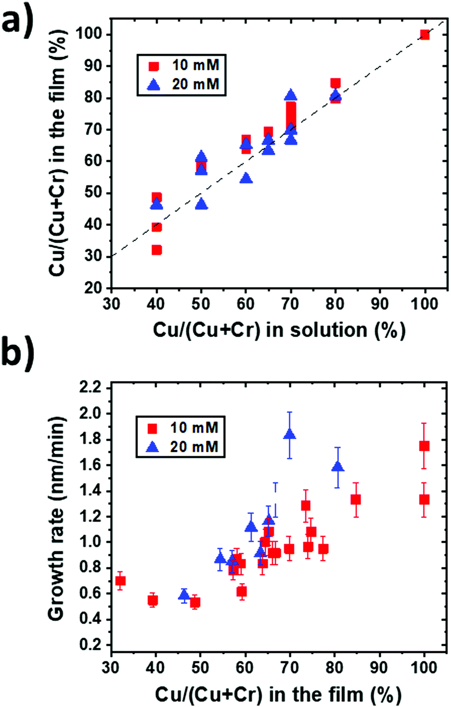 | ||
| Fig. 1 (a) Cu/(Cu + Cr) cationic ratio in the film measured by EDS as a function of the cationic ratio in the solution for the depositions performed with 10 mM and 20 mM total cationic molar concentration solutions of series 1. (b) Growth rate as a function of the cationic ratio in the films for the depositions performed with 10 mM and 20 mM total cationic molar concentration solutions. The error bar represents the 10% relative error from SEM measurements. | ||
The film thickness measured from the SEM cross-section images allows calculating the deposition rate for different compositions. The growth rate as a function of the film composition is reported in Fig. 1b for the two total molar concentrations used for these experiments. In these deposition conditions, it is evidenced that the Cu-rich films grow faster, and generally, a higher total molar concentration leads to the synthesis of thicker films but not at twice the thickness. When increasing the concentration of the Cu precursor, the higher growth rate suggests that the decomposition of Cr(acac)3 and its reaction with Cu and O are catalysed by Cu(acac)2 and its by-products, in agreement with the deposition of CuCrO2 by PI-MOCVD,24 where a similar trend was found. Moreover, these results are coherent with the growth mechanism proposed for CuCrO2 deposited by spray pyrolysis25 as the film formation occurs by the consecutive stacking of CrO6 octahedra and O–Cu–O dumbbells. Initially, Cr is adsorbed until the surface is saturated. Successively, Cu(acac)2 decomposes and reacts with the Cr terminated surface until the surface is adequately Cu covered. Finally, the Cr atoms react with the Cu terminated surface allowing the film growth. A lack of Cu inhibits the formation of O–Cu–O dumbbells and the subsequent film growth, explaining the increasing growth rate with the Cu content.
These analyses allowed us to control the composition and thickness of the films and were used to synthesize the samples of series 2. The films were grown from the solution concentrations of Cu/(Cu + Cr) of 40%, 50%, 70% and 100%. Several runs lead to film compositions corresponding to 50 ± 5%, 63 ± 5%, 77 ± 5% and 100% of Cu. These samples will be labelled as CuCrO2:X in the following, with X corresponding to the Cu content (in %) in the films as measured by EDS.
Structural properties
The structural properties of the CuCrO2:X films of series 2 were investigated by XRD. In Fig. 2a, XRD patterns were compared with the ICDD reference patterns of the rhombohedral CuCrO2 delafossite structure (space group R![[3 with combining macron]](https://www.rsc.org/images/entities/char_0033_0304.gif) m, ICDD 04-010-3330) and cubic Cu2O (space group Pnm, ICDD 00-005-0667), presented in the top windows. The stoichiometric CuCrO2:50% pattern, as shown in Fig. 2a(1), shows two wide peaks at 2θ = 36.4° and 2θ = 62.4°. They can be assigned to the (012) and (110) reflections of CuCrO2. The broadness of these peaks indicates a poor crystallinity. The weak band in the 40–50° range is attributed to the glass substrate.37 The Cu-rich CuCrO2: 63% pattern (Fig. 2a(2)) shows only one narrow (012) peak, thus suggesting a higher crystallization and an increase of grain size. These results are in good agreement with the previous report on Cr-deficient CuCrO2,30 where the authors reported a change in the preferred crystal orientation from the (006) plane to the (012) plane with an increase of Cr deficiency. Increasing the copper content up to the CuCrO2:77%, the composition (Fig. 2a(3)) leads to the additional formation of a Cu2O cubic phase as stated by the presence of the Cu2O (200) reflection at 2θ = 42°, in agreement with the pattern of the Cu2O film synthesized under the same deposition conditions (Fig. 2a(4)). This result highlights the deposition of the solid solution composed of Cu2O and CuCrO2. The overall poor crystallinity of our samples is attributed to the low deposition temperature and atmospheric pressure used during the synthesis. These results allow us to classify the thin films of series 2 in 4 categories: stoichiometric CuCrO2, Cu-rich CuCrO2, Cu2O + CuCrO2 and Cu2O.
m, ICDD 04-010-3330) and cubic Cu2O (space group Pnm, ICDD 00-005-0667), presented in the top windows. The stoichiometric CuCrO2:50% pattern, as shown in Fig. 2a(1), shows two wide peaks at 2θ = 36.4° and 2θ = 62.4°. They can be assigned to the (012) and (110) reflections of CuCrO2. The broadness of these peaks indicates a poor crystallinity. The weak band in the 40–50° range is attributed to the glass substrate.37 The Cu-rich CuCrO2: 63% pattern (Fig. 2a(2)) shows only one narrow (012) peak, thus suggesting a higher crystallization and an increase of grain size. These results are in good agreement with the previous report on Cr-deficient CuCrO2,30 where the authors reported a change in the preferred crystal orientation from the (006) plane to the (012) plane with an increase of Cr deficiency. Increasing the copper content up to the CuCrO2:77%, the composition (Fig. 2a(3)) leads to the additional formation of a Cu2O cubic phase as stated by the presence of the Cu2O (200) reflection at 2θ = 42°, in agreement with the pattern of the Cu2O film synthesized under the same deposition conditions (Fig. 2a(4)). This result highlights the deposition of the solid solution composed of Cu2O and CuCrO2. The overall poor crystallinity of our samples is attributed to the low deposition temperature and atmospheric pressure used during the synthesis. These results allow us to classify the thin films of series 2 in 4 categories: stoichiometric CuCrO2, Cu-rich CuCrO2, Cu2O + CuCrO2 and Cu2O.
 | ||
| Fig. 2 (a) XRD pattern of the (1) stoichiometric CuCrO2, (2) Cu-rich CuCrO2, (3) Cu2O + CuCrO2 and (4) Cu2O films. The top windows show the ICDD references (ICDD 04-010-3330) for CuCrO2 and (ICDD 00-005-0667) for Cu2O. (b) Raman spectra of the same films. | ||
Raman spectroscopy was used on the same samples to confirm this hypothesis. Raman spectra are shown in Fig. 2b. Our stoichiometric and Cu-rich CuCrO2 samples are characterized by the three Raman modes at 101 cm−1, 460 cm−1, and 709 cm−1 (triangles in Fig. 2b(1) and (2)), assigned to the Eu, Eg, and A1g modes of CuCrO2, respectively, in agreement with the previous report on this material.38 Additional modes are attributed to the presence of defects able to relax the Raman selection rules. The first one labelled with * and observed in the range of 500–670 cm−1 is attributed to the presence of intrinsic defects.39 Its intensity increases with Cu content, suggesting a greater amount of defects for Cu-rich CuCrO2 when compared to the stoichiometric CuCrO2. The second one, at 770 cm−1, labelled as ■, has not been reported before and further investigations are required for its assignment. Cu2O modes are expected at 108 cm−1, 149 cm−1, 216 cm−1, 495 cm−1 and 649 cm−140 and the CuO modes at 297 cm−1, 347 cm−1, and 632 cm−1.41 The absence of the CuO and Cu2O Raman modes in these samples confirms that Cu-based oxides are either absent or amorphous and dispersed in CuCrO2 films, in agreement with the XRD results. The successful deposition of the crystallized non-stoichiometric CuCrO2 without any detectable secondary phase in the films of the Cu composition of up to 63% is achieved. Further results presented in the next section (Fig. 4c) confirm the presence of Cu2O in the films with a Cu/(Cu + Cr) of > 65%.
For the Cu2O + CuCrO2 composite film (Fig. 2b(3)), the Raman modes at 99 cm−1 is attributed to the Eu mode of the delafossite phase. Additional modes are assigned to Cu2O, as confirmed by the spectrum of the Cu2O film deposited under the same conditions (Fig. 2b(4)). The formation of Cr oxides is excluded due to the Cu-rich/Cr-poor environment used for the growth.
Thus, the classification of the samples of series 2 is well confirmed, allowing us to label as the stoichiometric CuCrO2, films with a Cu composition of ∼50%, Cu-rich CuCrO2 with a Cu composition of ∼65%, Cu2O + CuCrO2 with a Cu composition of ∼77%, and Cu2O.
The films corresponding to the out of stoichiometry composition of CuCr0.58OX (Cu/(Cu + Cr) = 63%) are characterized by a greater amount of defects in comparison with the stoichiometric compound. The preservation of the crystalline delafossite phase within a wide variation in the cationic ratio is consistent with previous reports on the Cu0.66Cr1.33O2 (Cu/(Cu + Cr) of 33%) by DLI-MOCVD42 and PI-MOCVD.24 Moreover, it is important to note that CuO is not detected in any of our films, despite Cu2+ being present in the starting precursor. As described in the work by Lim et al.,43 the gas phase decomposition of Cu(acac)2 results in the formation of metallic copper condensing on the substrate. Then, Cu0 oxidizes to Cu2O. When the oxygen partial pressure is too high during the growth, Cu2O undergoes a secondary oxidation reaction to form CuO. The direct oxidation of Cu0 to Cu2+ is excluded because the Cu oxidation state transforms successively from Cu0 to Cu1+ and then to Cu2+.44 Thus, the absence of Cu0 and CuO in our films demonstrates that the used oxygen partial pressure is adequately high to completely oxidize Cu0 to Cu1+, while still sufficiently low to prevent the formation of CuO. The reaction with Cr can also be a stabilising factor for Cu1+. Furthermore, the deposition of a composite material formed solely by Cu2O and CuCrO2 is in agreement with the phase diagram of the Cu–Cr–O system under these deposition conditions.45 As shown by the thermodynamic results, the use of a low oxygen partial pressure allows the coexistence of Cu2O and CuCrO2 phases, preventing the formation of CuO, which would be detrimental for the synthesis of transparent conductive materials.
Morphology and microstructure
Morphological and microstructural properties of the films are critical parameters for their integration into devices. The evolution of the morphology and grain size with the composition for the samples of series 2 with a similar thickness is presented in Fig. 3. Stoichiometric CuCrO2 (Fig. 3a) presents a dense and close-packed morphology with small well-defined grains, whereas an irregular grain shape with an overall increase in grain size is observed in Cu-rich CuCrO2 (Fig. 3b), in agreement with the XRD results. The Cu2O + CuCrO2 composite film (Fig. 3c) is composed of more rounded grains with a heterogeneous shape. | ||
| Fig. 3 Top view and cross-section (inset) SEM micrographs of the films of series 2. (a) The stoichiometric CuCrO2, (b) Cu-rich CuCrO2 and (c) Cu2O + CuCrO2 samples. The scale bar is given on each micrograph. | ||
Cross-section images in insets clearly show the similar thickness of the three films and a variation of the superficial roughness with the Cu/(Cu + Cr) cationic ratio, with a maximum roughness for Cu-rich CuCrO2. The AFM measurements confirmed the trend of the roughness with values of root mean square roughness of 0.99 ± 0.15 nm, 2.08 ± 0.35 nm and 1.42 ± 0.18 nm for CuCrO2:59%, CuCrO2:65% and Cu2O + CuCrO2:77% films, respectively.
The microstructure of two Cu-rich films, CuCrO2:59% and CuCrO2:65%, and of the Cu2O + CuCrO2:73% composite film was analysed using TEM. HRTEM images and SAED patterns are presented in Fig. 4. The Cu-rich CuCrO2 thin films present a nanocolumnar microstructure with a broad orientation distribution, as reported previously by our group.16 The increase of the Cu content leads to the growth of wider grains with higher vertical alignment, as visible by the comparison between CuCrO2:59% (Fig. 4a) and CuCrO2:65% (Fig. 4b). These results are in good agreement with SEM observations, as the growth of bigger nanocolumnar grains is likely related to the increase in the superficial roughness for the Cu-rich films. SAED patterns confirm that both films crystallize in the CuCrO2 structure without any detectable secondary phase, in agreement with the Raman and XRD results. This result corroborates that there is a wide compositional range, up to Cu/(Cu + Cr) = 65%, in which the crystalline delafossite phase is preserved despite the variation of stoichiometry.
 | ||
| Fig. 4 Microstructural characterisation by TEM of the Cu-rich CuCrO2 films. From the left, cross-section HRTEM in the dark mode, cross-section HRTEM in the bright mode and SAED patterns for the (a) CuCrO2:59%, (b) CuCrO2:65% and (c) Cu2O + CuCrO2 (Cu/(Cu + Cr) = 73%) samples. The corresponding SAED patterns identifying the CuCrO2 rhombohedral delafossite phase and the Cu2O cubic phase are presented along with the theoretical diffraction patterns of the present phases as computed with the software JEMS. | ||
For the Cu2O + CuCrO2:73% nanocomposite film (Fig. 4c), the formation of the secondary Cu2O phase results in more rounded grains. The film is composed of both Cu2O and CuCrO2 as confirmed by SAED, which is consistent with the Raman and XRD results.
Surface chemistry analysis
XPS was used to determine the chemical state of the different elements in the bulk of the films by the analysis of Cu 2p (Fig. 5a) and Cr 2p (Fig. 5b) contributions. The evolution of the intensity with Cu/(Cu + Cr), increasing for Cu 2p3/2 and decreasing for Cr 2p3/2, suggests an increase in the Cu content and a reduction in the Cr content, in agreement with the EDS quantification. The spectra from the Cu 2p3/2 core level (Fig. 5a) are similar for all the samples. They are characterized by a moderate intensity of Cu(II) satellite peaks between 940 eV and 945 eV. This feature is associated with the Cu2+ state. The main peak is centred at 932.6 eV. The fitting of this peak for the three samples is shown in Fig. S1 in the ESI.† This contribution can be ambiguously attributed to Cu0 and Cu1+ due to their close binding energies centred at 932.5 eV and 932.6 eV, respectively. The width of the peak (FWHM ≈ 1.2 eV) suggests the presence of Cu in the monovalent state. Besides, a small contribution of Cu2+ (FWHM ≈ 2.0 eV), centred at 933.7 eV, is present in the bulk of the samples as confirmed by the asymmetry of the Cu 2p3/2 peak towards higher binding energies.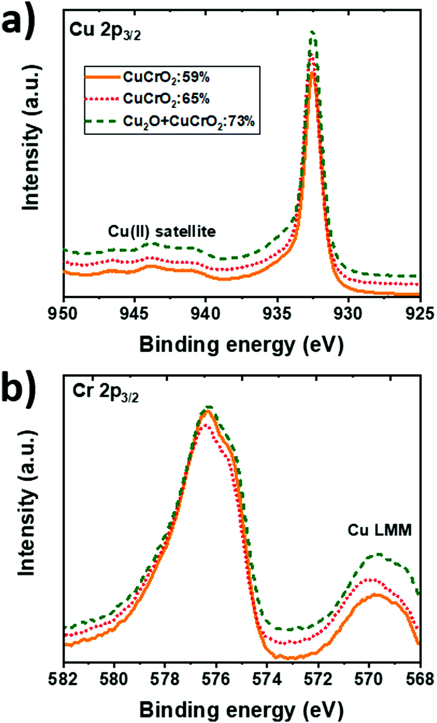 | ||
| Fig. 5 XPS spectra in the (a) Cu 2p3/2 and (b) Cr 2p3/2 orbitals energy ranges for CuCrO2:59%, CuCrO2:65% and Cu2O + CuCrO2 (Cu/(Cu + Cr) = 73%). The spectra were shifted for clarity. | ||
The Cr 2p3/2 core level (Fig. 5b) is centred at a binding energy of 576 eV corresponding to Cr3+ in agreement with the previous report on CuCrO2.24 Nevertheless, the distinction among the Cr species is complicated due to the presence of the Cu Auger peak, Cu LMM, centred at 569.9 eV. Again, the position of this Auger peak suggests the presence of Cu1+ rather than the metallic Cu,46 which should be centred at 568.3 eV.47 These results indicate that Cu and Cr are mainly in the 1+ and 3+ oxidation states, respectively, despite the stoichiometry variation. The O 1s peak (not shown here) was centred at around 530 eV.
The existence of Cu2+ does not necessarily imply the formation of CuO, not detected in our films, because it has been reported that Cu2+ can be present in the planar triangular network of the lattice, balanced by oxygen interstitial.18 This is in agreement with the results obtained by the combustion synthesis of CuCrO2+x,18 where the pure delafossite phase was detected despite the higher amount of Cu2+ species (37% Cu1+vs. 63% Cu2+). The presence of Cu2+ in our samples can be induced by the Cr deficiency, leading to an excess of holes at the Cu sites. This is supported by Ling et al.34 in the case of films obtained by the solid state reaction due to the fact that the Cu2+ content increases when the Cr content decreases. In our case, because of the O-poor environment used during the growth, the formation of Cu2+ is not favoured.
Table 1 presents the contribution in % of Cu1+ and Cu2+ to the Cu 2p3/2 spectra. The FWHM of the fitted peaks is also included in brackets. This procedure leads to a maximum value of the Cu1+/Cu2+ ratio of CuCrO2:65%. As proposed by Ling et al.,34 this fact suggests a favourable electronic structure with an improvement of hybridization between Cu 3d and O 2p orbitals. A more recent work by Singh et al.48 confirmed that the conduction mechanism takes place among Cu1+–O–Cu2+ sites, rather than directly between Cu1+ and Cu2+ sites. We can speculate that in both cases, with the conduction taking place via direct Cu1+–Cu2+ or via Cu1+–O–Cu2+ sites, the maximization of the Cu1+/Cu2+ ratio is required to increase the number of hopping sites and, thus, the film conductivity.
| Cu/(Cu + Cr) in the film by EDS (%) | Cu1+ (%) (FWHM) | Cu2+ (%) (FWHM) |
|---|---|---|
| 59 | 80 (1.26 eV) | 20 (2.05 eV) |
| 65 | 87 (1.25 eV) | 13 (2.05 eV) |
| 73 | 79 (1.22 eV) | 21 (2.04 eV) |
VB-XPS was performed on the Cu-rich film with a Cu/(Cu + Cr) of 65% (Fig. S2 in the ESI†) and was compared with the curve resulting from the band theory, adapted by the work of Yokobori et al.49 The theoretical spectra shows that the maximum of the valence band is dominated by the Cr 3d states (labelled with α) with a contribution attributed to the Cu 3d states (indicated with β), responsible for the peak with the highest intensity. Additional contributions at higher binding energies (labelled with γ) are attributed to the O 2p orbital. We can distinguish the 3 contributions in the experimental spectra, although the resolution of the spectrometer was too low to obtain additional information. The reduced intensity of the Cr states compared to that of the Cu ones can be attributed to the lower cross-section of the trivalent cation compared to Cu.50 However, we may speculate that the variation in intensities can also be linked to the Cu abundance/Cr deficiency in our films, leading to the limited presence of the shoulder of the Cr 3d states at about 1.5 eV. Consequently, we can assert that the Fermi level remains close to the top of the valence band, in agreement with the high charge density of delafossite oxides and with the previous report of VB-XPS for this compound.29 The use of a higher resolution XPS spectrometer will be essential to obtain a proper quantification of the energy difference between the Fermi level and the valence band edge.
Electrical measurements during annealing up to 200 °C under N2/O2 with 20% O2 (not shown here) were performed on a 200 nm thick sample with a Cu/(Cu + Cr) of 61%. The resistivity variation with the temperature was fitted using the Arrhenius equation, leading to an activation energy of 76 meV. This value ranges around 3 KbT, highlighting a highly degenerate semiconductor. This result is in good agreement with the proximity of the Fermi level with the top of the valence band as confirmed by our VB-XPS spectra.
Electrical properties
The impact of the stoichiometry on the electrical properties of the CuCrO2:X thin films is reported in Fig. 6 for all our samples (series 1 and series 2). The variation of the resistivity values with Cu/(Cu + Cr) in the film follows a U-shape curve, which was fitted using an exponential quadratic law as a guide for the eyes. The values related to the 4 sample categories of series 2 were marked with arrows. They prove that, for a given composition, the thickness variations are not strongly affecting the electrical properties. It is important to note that the minimum of the curve does not correspond to the stoichiometric samples but to the Cu-rich CuCrO2 ones. The lowest resistivity values, below 0.1 Ω cm, were obtained for the Cu-rich CuCrO2 films with a Cu/(Cu + Cr) value between 60 and 70%, corresponding to the Cu-rich CuCrO2 and Cu2O + CuCrO2 composite films, respectively. For more clarity, the graph has been divided in three regions: region 1, from Cu-poor CuCrO2 to the stoichiometric one, i.e. a Cu/(Cu + Cr) value from 40% to 50%; region 2, Cu-rich CuCrO2 with a Cu/(Cu + Cr) from 51% to 65%; and region 3 from the composite Cu2O + CuCrO2 to the pure Cu2O corresponding to a Cu/(Cu + Cr) from 66% to 100%. In region 1, Cu-poor CuCrO2 shows a very high resistivity value of around 1000 Ω cm, reduced down to 10 Ω cm for the stoichiometric samples, comparable with the values reported in the literature.13 In region 2, the resistivity is reduced by two orders of magnitude, reaching values below 0.1 Ω cm for Cu-rich CuCrO2 films with a Cu/(Cu + Cr) value between 60 and 65%. The lowest resistivity value of 0.02 Ω cm is achieved in region 3 for the Cu2O + CuCrO2 composite film with 67% of Cu. The electrical properties are then deteriorated up to the value around 100 Ω cm for the pure Cu2O.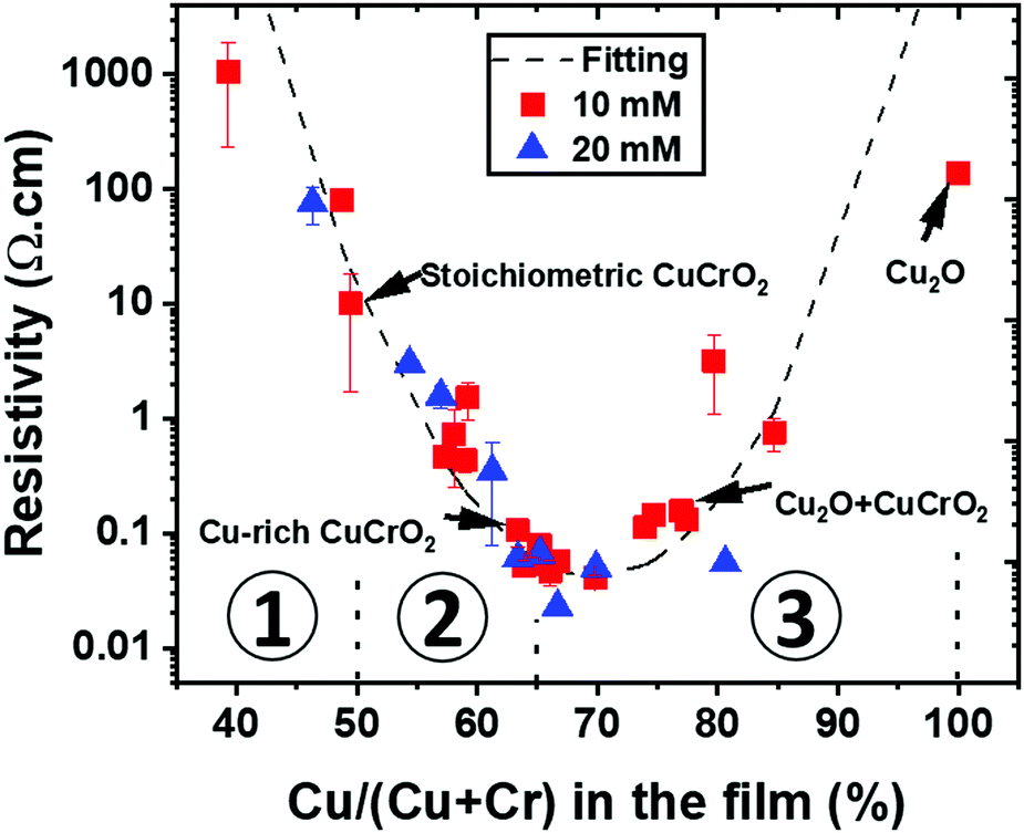 | ||
| Fig. 6 Variation of the resistivity with the cationic ratio in the out of stoichiometry CuCrO2 thin films. The values corresponding to the samples of series 2 are indicated by the arrows. | ||
The low conductivity of samples in region 1 can be attributed to their low crystallinity of the films for this composition. Although this is only a qualitative explanation, the enhancement of the conductivity of two orders of magnitude for samples with a composition in the 50–65% range can be confirmed through simultaneous factors as established by Chen et al.51 On the one hand, the increase in the cationic ratio can result in the formation of defects such as Cu vacancy and Cu antisite that have a lower formation energy than others.52 In our Cu-rich/Cr-deficient conditions, we infer that the additional Cu atoms might be placed in the Cr vacancies to form Cu antisite defects (CuCr). This will be balanced by the generation of holes, leading to an increase of the charge carrier density in the films,51 thus resulting in a lower resistivity of the film. Other defect species can play a major role in the electrical properties.
In region 2, the films within the 60–65% compositional range show an improved crystallinity as indicated by the higher intensity of the (012) reflection in XRD and the growth of bigger grains, as observed by SEM and TEM. This is congruent with the work by Sidik et al.30 where Cr deficiency was demonstrated to enhance the crystallinity of the films. Furthermore, as stated before, the enhancement of the conductivity can be attributed to the favourable electronic structure of these films through the maximization of the Cu1+/Cu2+ ratio, as proved by XPS. Nevertheless, the lowest resistivity value of 0.02 Ω cm was achieved in region 3 for the Cu2O + CuCrO2 composite film with 67% of Cu. Increasing the Cu content to above 65% favours, in our deposition conditions, the formation of the Cu2O phase in the delafossite phase that is more conductive, thus increasing the electrical resistivity up to the values obtained for the pure Cu2O. This increase can be attributed to the change in grain shape and degradation of the film crystallinity. In comparison, the films deposited by PI-MOCVD at low pressure with a similar composition resulted in the synthesis of CuO + Cu2O + CuCrO2,24 with a resistivity higher than that of the delafossite phase out of stoichiometry. This finally demonstrates that the fact to prevent the formation of CuO, as reported in our study, is promising for the synthesis of highly conductive films.
Out of stoichiometry CuCrO2 films with no detectable secondary phase are characterized by a low carrier mobility, being under the detection limit of our experimental setup. This allows setting an upper limit of 0.1 cm2 V−1 s−1 for these films. The Hall effect measurements were successfully performed for Cu2O + CuCrO2:73% and pure Cu2O, confirming the p-type behaviour of these films. The mobility values of 0.65 cm2 V−1 s−1 and 5 cm2 V−1 s−1 were obtained for these two samples, respectively. The corresponding charge carrier density values were 9.3 × 1018 cm−3 and 1.5 × 1016 cm−3, respectively. These results reveal an improvement in mobility by the formation of Cu2O. This finding allowed us to conclude that the lowest resistivity achieved for Cu2O + CuCrO2 with 67% of Cu is due to the combination of the good mobility of Cu2O and the high charge density achieved for CuCrO2.
Optical characterization and figure of merit
The optical properties of the samples of series 2 were probed by UV–vis spectroscopy and the results are reported in Fig. 7. As observed in Fig. 7a, the total transmittance is reduced when increasing the copper content. The average value in the 400–800 nm visible range is around 63% for the stoichiometric CuCrO2 film and decreases down to 45% for Cu2O. The reduced slope of the transmittance versus wavelength curve observed for the Cu2O + CuCrO2 sample is a further indication of the secondary phase in the film.53 The presence of another phase will create different optical transition levels, finally resulting in a smoother slope of the transmittance curve. The reflectance (Fig. 7b) does not follow any clear trend, with an average value in the 400–800 nm range varying from 26% for the Cu2O + CuCrO2 composite film to 32% for the Cu-rich CuCrO2 film. The shift of the reflectance minimum could be attributed to a variation of the refractive index with the composition. The absorbance was modelled taking into account multiple reflections within the thin films and a non-absorbing substrate.24 It should be noted that the direct band gap in CuCrO2 is responsible for the optical properties, whilst the indirect energy gap influences the electrical properties.54 A Tauc plot was used to estimate the direct energy gap (Fig. 7c), and the estimated values are around 3.2 and 3.15 eV for the stoichiometric CuCrO2 and Cu-rich CuCrO2, respectively, in agreement with the literature.12,25 The lowest optical properties obtained when increasing Cu/(Cu + Cr) suggests the stronger interaction between Cu 3d10 electrons responsible for the reduction of the energy gap and the overall transparency.55 The formation of Cu2O leads to an additional optical transition at around 2.5 eV, further reducing the energy gap, as observable for Cu2O + CuCrO2 with a value of around 3.1 eV. An energy gap of around 2.6 eV was obtained for the pure Cu2O, in agreement with previous studies on Cu2O films deposited by CVD.56 The presence of CuO would lead to the appearance of another optical transition at around 1.6 eV, not observable in our samples. | ||
| Fig. 7 Optical properties and figure of merit for the out of stoichiometry CuCrO2 films of series 2. (a) Transmittance, (b) reflectance, (c) Tauc plot, and (d) FoM by Gordon, FoMG, for the various compositions and the two total molar concentrations that were used (series 1) and the values estimated from the literature for various chemical deposition techniques. | ||
Despite thickness variations, the FoMG value was calculated from eqn (1) to compare the properties of our films with the literature; the results are reported in Fig. 7d. The FoMG values from the literature were estimated with a 0% reflectivity when this value is not reported in the study. The AA-MOCVD Cu-rich CuCrO2:65% films showed a promising FoMG value of 2200 μS, comparable with the value of 2300 μS, the highest for this material, obtained by the Cu-deficient CuCrO2 films deposited by PI-MOCVD.24 The AA-MOCVD growth method presents many advantages as it is performed at atmospheric pressure and at lower temperature than the PI-MOCVD method. Besides, the Cu2O + CuCrO2:67% composite films with higher conductivity achieved a good FoMG value of 1400 μS, despite a reduction in their optical performances.
Conclusions
AA-MOCVD is a versatile and reproducible procedure working at a low temperature (350 °C) and atmospheric pressure, which enables the deposition of highly transparent and conductive CuCrO2-based thin films.The deposition of the out of stoichiometry CuCrO2 films without any detectable secondary phase is achieved up to a composition of Cu/(Cu + Cr) of 65%. Single-phase Cu-rich CuCrO2 films present a nanocolumnar microstructure with a resistivity value lower than 0.1 Ω cm, and a wide band gap of around 3.1–3.2 eV. The optimal composition was found for Cu-rich CuCrO2:65% with a resistivity value of 0.05 Ω cm and an average transmittance of 55% in the 400–800 nm range, resulting in a high p-type FoMG value of 2200 μS. The enhancement of p-type conductivity is attributed to the formation of the intrinsic defects with Cu, occupying the Cr vacancies and creating Cu antisite defects, and to the further improvement of the film crystallinity.
In summary, we highlight the successful deposition of the Cr- deficient CuCrO2 by AA-MOCVD with a figure of merit comparable with the one of the Cu-deficient CuCrO2 films. Besides, the growth in an oxygen-poor environment has been demonstrated to impede the formation of CuO, allowing the synthesis of nanocomposite films composed exclusively of Cu2O and CuCrO2. These films are characterized by a carrier mobility of 0.65 cm2 V−1 s−1, higher than the Cu-rich CuCrO2 films. In this study, the lowest resistivity value of 0.02 Ω cm was achieved for the Cu2O + CuCrO2 films with 67% of Cu. Despite a reduced average transmittance of 52%, the performance of the nanocomposite films led to a FoMG value of 1400 μS.
As revealed in the present work, the modulation of the optical and electrical properties, such as mobility, resistivity, total transmittance, and band gap, is achieved by tuning the stoichiometry of the films. This allowed us to synthesize two appealing candidates for hole transport layers in the thin film, organic, and perovskite solar cells, as well as for organic light-emitted diodes (OLEDs) and thin film transistors (TFTs) as these Cu-rich CuCrO2 thin films can be incorporated into these devices.
Conflicts of interest
There are no conflicts to declare.Acknowledgements
L. Bottiglieri acknowledges the French Ministry of Higher Education and Research for funding his PhD scholarship. This research has benefited from the characterization equipment of the Grenoble INP – CMTC platform supported by the Centre of Excellence of Multifunctional Architectured Materials “CEMAM” noANR-10-LABX-44-01 funded by the “Investments for the Future” Program. This work was funded by the Agence Nationale de la Recherche (ANR, France) via the program ANR-17-CE05-0034 (Oxygene). This work benefited from the facilities and expertise of the (OPE)N(RA characterization platform of the FMNT (FR 2542)) supported by CNRS, Grenoble INP and UGA.References
- R. G. Gordon, Criteria for choosing transparent conductors, MRS Bull., 2000, 25, 52–57 Search PubMed.
- A. Bhorde, et al., (400)-Oriented indium tin oxide thin films with high mobility and figure of merit prepared by radio frequency magnetron sputtering, Thin Solid Films, 2020, 704, 137972 Search PubMed.
- S. Yu, et al., Fabrication of p-type SnO2 films via pulsed laser deposition method by using Sb as dopant, Appl. Surf. Sci., 2013, 286, 417–420 Search PubMed.
- S. Yu, et al., Electrical and photoelectric properties of transparent Li-doped ZnO/ZnO homojunctions by pulsed laser deposition, Thin Solid Films, 2013, 540, 146–149 Search PubMed.
- H. Kawazoe, et al., P-type electrical conduction in transparent thin films of CuAlO2, Nature, 1997, 389, 939–942 Search PubMed.
- T. Zhao, M. Hasegawa and H. Takei, Crystal growth and characterization of cuprous ferrite (CuFeO2), J. Cryst. Growth, 1996, 166, 408–413 Search PubMed.
- P. Rattanathrum, C. Taddee, N. Chanlek, P. Thongbai and T. Kamwanna, Structural and physical properties of Ge-doped CuCrO2 delafossite oxide, Ceram. Int., 2017, 43, S417–S422 Search PubMed.
- K. Ueda, et al., Epitaxial growth of transparent p-type conducting CuGaO2 thin films on sapphire (001) substrates by pulsed laser deposition, J. Appl. Phys., 2001, 89, 1790–1793 Search PubMed.
- S. Mahapatra and S. A. Shivashankar, Low-pressure metal–organic CVD of transparent and p-type conducting CuCrO2 thin films with high conductivity, Chem. Vap. Deposition, 2003, 9, 238–240 Search PubMed.
- M. K. Jayaraj, A. D. Draeseke, J. Tate and A. W. Sleight, p-Type transparent thin films of CuY1−xCaxO2, Thin Solid Films, 2001, 397, 244–248 Search PubMed.
- N. Duan, A. W. Sleight, M. K. Jayaraj and J. Tate, Transparent p-type conducting CuScO2+x films, Appl. Phys. Lett., 2000, 77, 2–4 Search PubMed.
- D. O. Scanlon and G. W. Watson, Understanding the p-type defect chemistry of CuCrO2, J. Mater. Chem., 2011, 21, 3655 Search PubMed.
- T. S. Tripathi, J.-P. Niemelä and M. Karppinen, Atomic layer deposition of transparent semiconducting oxide CuCrO2 thin films, J. Mater. Chem. C, 2015, 3, 8364–8371 Search PubMed.
- J. Wang, Y. J. Lee and J. W. P. P. Hsu, Sub-10 nm Copper Chromium Oxide Nanocrystals As Solution Processed P-Type Hole Transport Layer For Organic Photovoltaics, J. Mater. Chem. C, 2016, 4, 3607–3613 Search PubMed.
- D. Xiong, et al., Hydrothermal synthesis of ultrasmall CuCrO2 nanocrystal alternatives to NiO nanoparticles in efficient p-type dye-sensitized solar cells, J. Mater. Chem., 2012, 22, 24760–24768 Search PubMed.
- T. Cossuet, et al., ZnO/CuCrO2 Core–Shell Nanowire Heterostructures for Self-Powered UV Photodetectors with Fast Response, Adv. Funct. Mater., 2018, 28, 1–12 Search PubMed.
- S. Zhou, et al., Room temperature ozone sensing properties of p-type CuCrO2 nanocrystals, Sens. Actuators, B, 2009, 143, 119–123 Search PubMed.
- J. Wang, et al., Combustion Synthesis of p-Type Transparent Conducting CuCrO2+x and Cu:CrOx Thin Films at 180 °C, ACS Appl. Mater. Interfaces, 2018, 10, 3732–3738 Search PubMed.
- S. Nie, et al., Solution-processed ternary p-type CuCrO2 semiconductor thin films and their application in transistors, J. Mater. Chem. C, 2018, 6, 1393–1398 Search PubMed.
- F. Jlaiel, M. Amami, N. Boudjada, P. Strobel and A. Ben Salah, Metal transition doping effect on the structural and physical properties of delafossite-type oxide CuCrO2, J. Alloys Compd., 2011, 509, 7784–7788 Search PubMed.
- Z. Y. Liu, G. Y. Wang, X. P. Liu and Y. J. Wang, Preparation of CuCrO2 and the photocatalytic properties of its composites, J. Fuel Chem. Technol., 2013, 41, 1473–1480 Search PubMed.
- A. Barnabé, Y. Thimont, M. Lalanne, L. Presmanes and P. Tailhades, p-Type conducting transparent characteristics of delafossite Mg-doped CuCrO2 thin films prepared by RF-sputtering, J. Mater. Chem. C, 2015, 3, 6012–6024 Search PubMed.
- D. C. Tsai, et al., Influence of chemical composition on phase transformation and optoelectronic properties of Cu-Cr-O thin films by reactive magnetron sputtering, J. Mater. Res. Technol., 2019, 8, 690–696 Search PubMed.
- J. Crêpellière, et al., Transparent conductive CuCrO2 thin films deposited by pulsed injection metal organic chemical vapor deposition: Up-scalable process technology for an improved transparency/conductivity trade-off, J. Mater. Chem. C, 2016, 4, 4278–4287 Search PubMed.
- L. Farrell, et al., Synthesis of nanocrystalline Cu deficient CuCrO2 – a high figure of merit p-type transparent semiconductor, J. Mater. Chem. C, 2016, 4, 126–134 Search PubMed.
- R. I. Sánchez-Alarcón, et al., Ultrasonic spray-pyrolyzed CuCrO2 thin films, J. Phys. D: Appl. Phys., 2016, 49, 175102 Search PubMed.
- H. Y. Chen, K. P. Chang and C. C. Yang, Characterization of transparent conductive delafossite-CuCr1−xO2 films, Appl. Surf. Sci., 2013, 273, 324–329 Search PubMed.
- S. Jeong, S. Seo and H. Shin, P-Type CuCrO2 particulate films as the hole transporting layer for CH3NH3PbI3 perovskite solar cells, RSC Adv., 2018, 8, 27956–27962 Search PubMed.
- D. Shin, J. S. Foord, R. G. Egdell and A. Walsh, Electronic structure of CuCrO2 thin films grown on Al2O3(001) by oxygen plasma assisted molecular beam epitaxy, J. Appl. Phys., 2012, 112, 113718 Search PubMed.
- U. Sidik, J. H. Kim, H.-K. Kim, H. Y. Lee and J. Lee, Structures and characteristics of delafossite CuCr1−xO2 thin films prepared by pulsed laser deposition, Micro Nano Lett., 2014, 9, 854–857 Search PubMed.
- S.-S. Lin, et al., The Optoelectronic Properties of p-Type Cr-Deficient Cu[Cr0.95−xMg0.05]O2 Films Deposited by Reactive Magnetron Sputtering, Materials, 2020, 13, 2376 Search PubMed.
- P. Lunca-Popa, et al., Tuning the electrical properties of the p-type transparent conducting oxide Cu1−xCr1+xO2 by controlled annealing, Sci. Rep., 2018, 8, 1–8 Search PubMed.
- P. Lunca Popa, J. Crêpellière, P. Nukala, R. Leturcq and D. Lenoble, Invisible electronics: Metastable Cu-vacancies chain defects for highly conductive p-type transparent oxide, Appl. Mater. Today, 2017, 9, 184–191 Search PubMed.
- D. C. Ling, C. W. Chiang, Y. F. Wang, Y. J. Lee and P. H. Yeh, Effect of Cr deficiency on physical properties of triangular-lattice antiferromagnets CuCr1−xO2 (0 ≤ x ≤ 0.10), J. Appl. Phys., 2011, 109, 30–32 Search PubMed.
- C. V. de Oliveira, et al., Structural and microstructural analysis of bifunctional TiO2/Al–Zr thin film deposited by hybrid process, Thin Solid Films, 2020, 709, 138255 Search PubMed.
- J. V. Hoene, R. G. Charles and W. M. Hickam, Thermal Decomposition of Metal Acetylacetonates: Mass Spectrometer Studies, J. Phys. Chem., 1958, 62, 1098–1101 Search PubMed.
- T. Chiu, K. Tonooka and N. Kikuchi, Preparation of transparent p-CuCrO2: Mg/n-ZnO heterojucntion with in situ laser anealing, SAW Futur. Mob. Comm. Syst., 2004, 2–4 Search PubMed.
- M. Han, et al., Effect of annealing temperature on structural, optoelectronic properties and interband transitions of CuCrO2 nanocrystalline films prepared by the sol-gel method, J. Alloys Compd., 2015, 647, 1028–1034 Search PubMed.
- M. Han, et al., Raman scattering measurements of phonon anharmonicity in the delafossite CuGa1−xCrxO2 (0 ≤ x ≤ 1) films, J. Raman Spectrosc., 2020, 51, 851–859 Search PubMed.
- L. Bergerot, C. Jiménez, O. Chaix-Pluchery, L. Rapenne and J. L. Deschanvres, Growth and characterization of Sr-doped Cu2O thin films deposited by metalorganic chemical vapor deposition, Phys. Status Solidi A, 2015, 212, 1735–1741 Search PubMed.
- A. Khan, C. Jiménez, O. Chaix-Pluchery, H. Roussel and J. L. Deschanvres, In situ Raman spectroscopy and X-ray diffraction studies of the structural transformations leading to the SrCu2O2 phase from strontium–copper oxide thin films deposited by metalorganic chemical vapor deposition, Thin Solid Films, 2013, 541, 136–141 Search PubMed.
- P. Lunca Popa, J. Crêpellière, R. Leturcq and D. Lenoble, Electrical and optical properties of Cu–Cr–O thin films fabricated by chemical vapour deposition, Thin Solid Films, 2016, 612, 194–201 Search PubMed.
- S. H. Lim, S. Desu and A. C. Rastogi, Chemical spray pyrolysis deposition and characterization of p-type CuCr1−xMgxO2 transparent oxide semiconductor thin films, J. Phys. Chem. Solids, 2008, 69, 2047–2056 Search PubMed.
- A. G. Nasibulin, I. S. Altman and E. I. Kauppinen, Semiempirical dynamic phase diagrams of nanocrystalline products during copper(II) acetylacetone vapour decomposition, Chem. Phys. Lett., 2003, 367, 771–777 Search PubMed.
- K. T. Jacob, G. M. Kale and Y. Waseda, Gibbs energy of formation of CuCrO4 and phase relations in the system Cu–Cr–O below 735 K, Thermochim. Acta, 1992, 208, 341–348 Search PubMed.
- Y. Ma, X. Zhou, Q. Ma and A. Litke, Photoelectrochemical Properties of CuCrO2: Characterization of Light Absorption and Photocatalytic H2 Production Performance, Catal. Lett., 2014, 144, 1487–1493 Search PubMed.
- I. Platzman, R. Brener, H. Haick and R. Tannenbaum, Oxidation of polycrystalline copper thin films at ambient conditions, J. Phys. Chem. C, 2008, 112, 1101–1108 Search PubMed.
- S. B. Singh, et al., Correlation between p-type conductivity and electronic structure of Cr-deficient CuCr1−x O2 (x = 0–0.1), Phys. Rev. B: Condens. Matter Mater. Phys., 2012, 86, 1–6 Search PubMed.
- T. Yokobori, et al., Electronic structure of the hole-doped delafossite oxides CuCr1−xMgxO2, Phys. Rev. B: Condens. Matter Mater. Phys., 2013, 87, 195124 Search PubMed.
- T. Arnold, et al., X-Ray spectroscopic study of the electronic structure of CuCrO2, Phys. Rev. B: Condens. Matter Mater. Phys., 2009, 79, 1–9 Search PubMed.
- H. Y. Chen, W. J. Yang and K. P. Chang, Characterization of delafossite-CuCrO2 thin films prepared by post-annealing using an atmospheric pressure plasma torch, Appl. Surf. Sci., 2012, 258, 8775–8779 Search PubMed.
- D. O. Scanlon and G. W. Watson, Conductivity limits in CuAlO2 from screened-hybrid density functional theory, J. Phys. Chem. Lett., 2010, 1, 3195–3199 Search PubMed.
- R. S. Yu and C. P. Tasi, Structure, composition and properties of p-type CuCrO2 thin films, Ceram. Int., 2014, 40, 8211–8217 Search PubMed.
- E. Chikoidze, et al., Control of p-type conduction in Mg doped monophase CuCrO2 thin layers, J. Phys. D: Appl. Phys., 2016, 49, 205107 Search PubMed.
- N. Zhang, J. Sun and H. Gong, Transparent p-Type Semiconductors: Copper-Based Oxides and Oxychalcogenides, Coatings, 2019, 9, 137 Search PubMed.
- J. Resende, C. Jiménez, N. D. Nguyen and J. L. Deschanvres, Magnesium-doped cuprous oxide (Mg:Cu2O) thin films as a transparent p-type semiconductor, Phys. Status Solidi A, 2016, 213, 2296–2302 Search PubMed.
Footnote |
| † Electronic supplementary information (ESI) available. See DOI: 10.1039/d1ma00156f |
| This journal is © The Royal Society of Chemistry 2021 |