
 Open Access Article
 This Open Access Article is licensed under a
 Creative Commons Attribution 3.0 Unported Licence
Exotic physical properties of 2D materials modulated by moiré superlattices
Beibei
Shi
,
Pengfei
Qi
 ,
Meiling
Jiang
,
Yuchen
Dai
,
Feng
Lin
,
Han
Zhang
and
Zheyu
Fang
*
,
Meiling
Jiang
,
Yuchen
Dai
,
Feng
Lin
,
Han
Zhang
and
Zheyu
Fang
*
School of Physics, State Key Lab for Mesoscopic Physics, Academy for Advanced Interdisciplinary Studies, Collaborative Innovation Center of Quantum Matter, and Nano-Optoelectronics Frontier Center of Ministry of Education, Peking University, Beijing 100871, China. E-mail: zhyfang@pku.edu.cn
First published on 8th July 2021
Abstract
van der Waals heterostructures of two-dimensional materials are naturally endowed with the nanoscale moiré pattern, which has become a versatile platform for studying novel quantum phenomena during the past few decades. Here, we discussed the moiré superlattice combining graphene and hexagonal boron nitride (h-BN) which led to the observation of electronic minibands, superlattice Dirac points and anomalous physical phenomena such as the quantum Hall effect and the Hofstadter butterfly pattern. The twist bilayer graphene (TBG) system has witnessed the appearance of angle-dependent van Hove singularities. Moreover, in the magic-angle twisted bilayer graphene (MATBG), there is a superconductor–insulator transition due to the enhancement of van der Waals forces by interlayer resonant conditions. Besides, owing to the moiré superlattice constant being comparable to the Bohr radius of excitons, exciton physics dominated by the moiré potential for the heterojunction based on transition metal dichalcogenide (TMD) monolayers has attracted extensive attention. This review mainly covers the exotic physical properties, ranging from electronic structures to excitonic properties of graphene-based and TMD-based van der Waals-coupled twistronic materials, and discusses the remaining unsolved strongly correlated questions and possible expected semiconductor device applications in the quantum matter world.
 Beibei Shi | Beibei Shi received her BS degree in physics from Hebei Normal University, China in 2017. She is currently pursuing her PhD (2017–) under the supervision of Prof. Zheyu Fang at Peking University. Her research focuses on the first-principles calculations on 2D materials and two-dimensional excitons of TMD twistronics. |
 Pengfei Qi | Pengfei Qi is currently a Boya post-doctoral research fellow in the School of Physics, Peking University, Beijing, China. He received his Master's degree in Condensed Physics from Nankai University in 2016 and his PhD degree in Optical Engineering from Nankai University in 2019. His current research interests mainly focus on the non-equilibrium dynamics and applications of two-dimensional excitons. |
 Zheyu Fang | Zheyu Fang is a professor in the School of Physics, Peking University, China. He received his PhD in Physics from Peking University and worked as a postdoc at Rice University with Prof. Naomi J. Halas and Prof. Peter Nordlander. He joined Peking University in 2012. His current research interests are plasmonics, near-field optics, and nanophotonic materials and devices. |
1. Introduction
Two-dimensional (2D) materials have become the most popular material system since 2004 when graphene was mechanically exfoliated from bulk graphite. Galvanized by this breakthrough, researchers have isolated and studied dozens of 2D crystals and predicted the existence of many more. These atomically layered materials that exhibit intriguing properties distinct from those of their bulk counterparts can be fabricated as building blocks for achieving advanced material properties. A so-called van der Waals (vdW)1 material is characterized by covalent bonding within the layer and weak vdW forces between the 2D plane. This has led many researchers to study the flatland regime of 2D materials ranging from fundamental physics2,3 to device applications such as high-performance photonic and optoelectronic devices.4–8 When two single layers are stacked with a rotation, they produce a moiré pattern of much larger length scale than the periodicity of each layer. The pattern is more often than not an incommensurate structure and exhibits twist-dependent emergent electronic behavior,9–12 whereas an overarching periodicity emerges in the local atomic registry of the constituent crystal structures, which is known as a moiré superlattice.13–18The moiré superlattice induced by the lattice mismatch or crystal orientation misalignment can significantly modify the electronic and optical properties of heterostructures.19 Graphene/hexagonal boron nitride (h-BN), a typical vdW heterostructure, exhibits greatly improved properties for device applications by stacking graphene on top of h-BN. In the graphene/h-BN heterostructure, the h-BN can reduce ripples and suppress charge inhomogeneities to improve the carrier mobility of graphene,20,21 as well as provide unique opportunities to open the band gap of graphene at the Dirac point by the periodic superlattice potential,13,22–27 which leads to various anomalous quantum phenomena including the quantum Hall effect and the Hofstadter butterfly pattern.13–15,28 Twisted bilayer graphene (TBG) is simply fabricated by changing the relative orientation between the layers, which induces low-energy Van Hove singularities (VHSs).29 This may provide intriguing prospects for VHS engineering of electronic phases. In some special cases, the two graphene layers are twisted relative to each other at a small angle which is called the magic angle, and there is a correlated insulator and unconventional superconductor transition due to the localization of electrons within the moiré superlattice.30,31
Although the distinctive linear dispersion of graphene yields unique electronic and optical properties, the zero-band gap greatly hinders its applicability in semiconductor based elements and devices. The TMD monolayer exfoliated from a bulk crystal possesses direct energy gaps in the range of 1–2 eV and opened up a new window for optoelectronics. The reduced dimensionality and the associated reduced dielectric screening result in a greatly enhanced exciton binding energy in monolayer TMDs. The strong excitonic effects lead to room temperature excitonic devices that have promising prospects for overcoming the dilemma of response time and integration in electron or/and photon based devices.32–34 Heterobilayers of TMDs are particularly attractive for low-dimensional semiconductor optics because they host interlayer excitons – with electrons and holes localized in different layers – and thereby possess various novel and appealing properties, especially in a typical type II band alignment, where electrons and holes find their energy minima in different layers.35–37 Besides, owing to the high sensitivity of TMDs to crystal structure symmetry and interlayer coupling, the bandgaps of TMD heterobilayers composed of various 2D materials are of big difference. Furthermore, the moiré potential determined by interlayer coupling in TMD heterobilayers can localize interlayer excitons and modulate the multiple interlayer exciton resonances, suggesting that the feasibility of engineering artificial excitonic crystals can provide a unique platform for studying novel quantum phases of matter.38–44
In this review, we mainly aim to describe exotic electronic and excitonic properties modulated by the nanoscale moiré pattern in graphene-based and TMD-based heterostructures. Firstly, we overview how the electronic structure of graphene is modified by the moiré superlattice and the anomalous quantum phenomena of graphene/h-BN. Then, we discuss the transport properties of twisted bilayer graphene. Moreover, the interplay of correlated insulating states and superconductivity of twisted bilayer graphene is also described. Finally, we review excitonic phenomena determined by the moiré potential in twisted TMD heterobilayers and come up with several possible perspectives to inspire the research enthusiasm for semiconductor quantum light-emitting devices based on moiré superlattices.
2. Quantum phenomena in the graphene moiré superlattice
Graphene has attracted great attention owing to its remarkable properties as the first 2D vdW material.45–48 The recent development of experimental techniques for combining graphene with other atomically thin vdW crystals has enabled the exploration of the properties of these so-called vdW heterostructures, which provides an exciting approach to design quantum materials that can harness and extend the already fascinating properties of the constituents. In this section, we first discuss the exotic experimental phenomena in the emergent graphene/h-BN moiré superlattice, such as superlattice Dirac points and Hofstadter butterfly spectrum. Then we illustrate the intriguing properties in twisted bilayer graphene (TBG) due to a stronger interlayer coupling than that in the graphene/h-BN moiré superlattice. Finally, we describe two correlated quantum states of correlated insulating states and unconventional superconductivity caused by a strong electron–electron Coulomb interaction in the magic-angle twisted bilayer moiré superlattice of graphene.2.1 Graphene/h-BN moiré superlattice
Heterostructures of 2D vdW materials offer a platform for engineering novel optoelectronic properties. h-BN is another well-known vdW material that is commonly used. It can provide high and homogeneous dielectric conditions for graphene, enabling the observation of the quantum Hall effect (QHE) and fractional quantum Hall effect (FQHE) in graphene/hBN heterostructures.49–51 Additionally, h-BN can modify the optoelectronic properties of graphene when aligned with graphene under certain circumstances, for example, the emergence of superlattice Dirac points, accompanied by the appearance of the Hofstadter butterfly spectrum.13–18,28 The graphene/h-BN heterostructure provides an opportunity for engineering the properties that can be achieved by tuning each of these degrees of freedom, thereby facilitating the design and realization of graphene-based devices. | (1) |
 | (2) |
 comes from the Berry phase, ν is the quantized filling factor of LLs and EF jumps by an amount of ge2/h. The longitudinal resistance Rxx is zero, while the Hall resistance Rxy exhibits a quantum Hall plateau, indicating that the system enters the quantum Hall regime (Fig. 1c). Note that σxy = −Rxy−1 and σxx = −Rxx−1. This Landau quantization is a result of the linear band dispersion of graphene. Additionally, the valley degree of freedom in graphene adds an extra twofold degeneracy, but, in most materials, the degeneracy of each LL is doubled due to the spin degree of freedom. Considering the valley and spin degrees of freedom of graphene, there are half-integer multiple quantum Hall plateaus, that is, the fractional quantum Hall effect. Fig. 1d shows an expanded view in the N = 0 LL between ν
![[thin space (1/6-em)]](https://www.rsc.org/images/entities/char_2009.gif) = 0 and ν = 1. Two-flux composite fermion states (centered around ν = 1/2) and four-flux composite fermion states (centered around ν = 1/4) are observed.54
= 0 and ν = 1. Two-flux composite fermion states (centered around ν = 1/2) and four-flux composite fermion states (centered around ν = 1/4) are observed.54
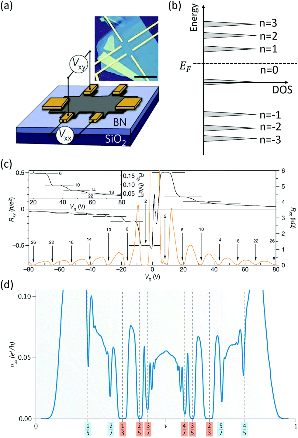 | ||
| Fig. 1 (a) Schematic of a Hall bar device made of graphene and h-BN used to measure the quantum Hall effect.52 Copyright 2011, Springer Nature Limited. (b) A schematic diagram of the DOS of LLs formed by quantization of Dirac fermions under an external perpendicular magnetic field.51 Copyright 2005, Springer Nature Limited. (c) Hall resistance (black) and magnetoresistance (orange) as a function of gate voltage under a fixed magnetic field and a low temperature. The upper inset is a diagram of a high-filling-factor plateau measured at different temperatures.51 Copyright 2005, Springer Nature Limited. (d) Device conductance (σxx) at B = 15 T between ν = 0 and ν = 1. The red labels indicate the 2-flux fractional quantum Hall effect and blue labels indicate the 4-flux sequence.55 Copyright 2019, Springer Nature Limited. | ||
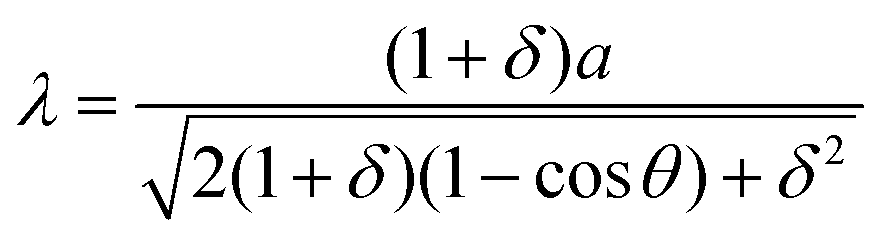 | (3) |
 | ||
| Fig. 2 (a) STM image of the moiré pattern observed in the graphene/h-BN heterostructure owing to the lattice mismatch between them. (b) The energy of the superlattice Dirac points as a function of moiré periodicity. The inset displays the wavelength of the moiré superlattice as a function of the twist angle (θ) between graphene and the h-BN substrate. (c) Schematic band structure of the graphene/h-BN heterostructure with a small twist angle. E, energy; k, momentum. (d) Measured bandgaps at the primary and superlattice Dirac points as a function of twist angle within a single graphene/h-BN device. Figure adapted with permission from: (a) ref. 25 Copyright 2014, Springer Nature Limited; (b) ref. 55 Copyright 2019, Springer Nature Limited; (c and d) ref. 59 Copyright 2018, AAAS. | ||
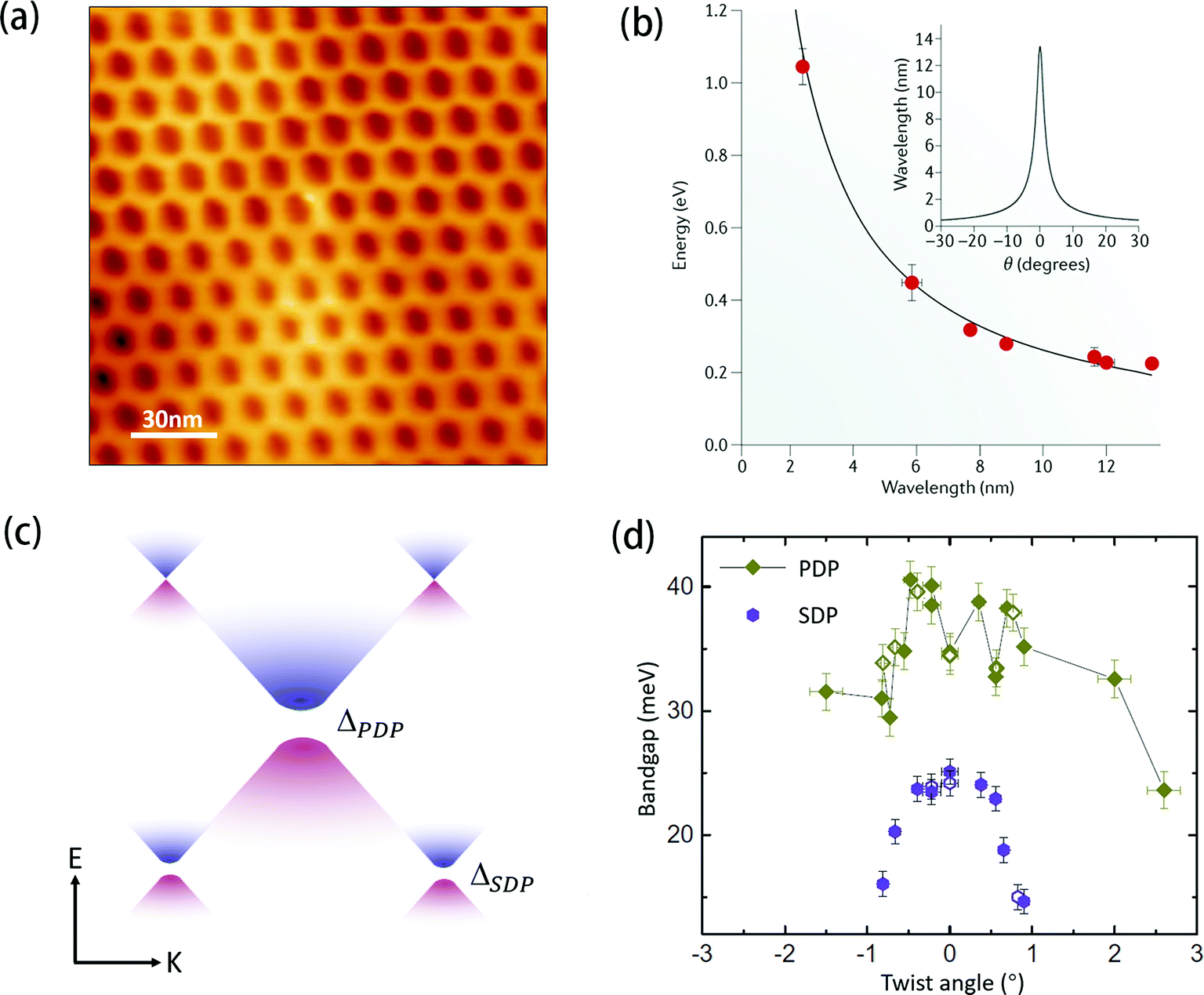
The long-period moiré pattern in the graphene/h-BN heterostructure provides a unique system to explore the interplay between electrical potentials and magnetic fields over similar length scales. The transport properties of graphene/h-BN devices indicate that the SDPs manifest themselves as additional peaks in the resistance symmetrically flanking the primary Dirac point.13–15 The charge carrier density n-dependent conductance measurements show that the longitudinal resistivity ρxx reaches a maximum at both sides of PDP and SDP (Fig. 3a), whereas the Hall resistivity ρxy drops suddenly at one side of the PDP and SDP and increases at the other side (Fig. 3b), reversing in sign. To present the detailed electronic structures of PDP and SDPs, the Rxx and Rxy are plotted as a function of gate voltage and magnetic field, which is called a Landau fan. The Landau fan diagram shows that the degeneracy of Landau levels formed by the two-dimensional electron gas increases and the system enters the quantum Hall state gradually as the magnetic field increases. Rxx reaches a minimum when the Fermi level crosses a LL and Rxy exhibits a quantum Hall plateau at the corresponding position. Similarly to the Dirac point, these SDPs break up into sequences of LLs when applying a magnetic field. Transport measurements show that these LLs emerge from each of these points, including PDP and SDPs, at low magnetic fields and intersect as the magnetic field increases, resulting in a series of energy levels, which is known as a Hofstadter butterfly spectrum (Fig. 3c and d).
 | ||
| Fig. 3 Emergence of anomalous quantum Hall states. Longitudinal resistivity ρxx (a) and Hall resistivity ρxy (b) plotted as a function of carrier density n. Positive values of n indicate electrons, and negative values indicate holes. Hall conductivity σxy plotted versus magnetic field B and gate bias Vg (c) and longitudinal resistance Rxx as a function of the magnetic field flux φ/φ0 and charge density n/n0 (d) in a graphene/h-BN device. (e) A simplified Wannier diagram in which the positions of the most prominent QHE states are plotted as a function of magnetic flux and charge carrier density. Figure adapted with permission from: (a and b) ref. 15 Copyright 2013, Springer Nature Limited; (c–e) ref. 18 Copyright 2015, AAAS. | ||
The Hofstadter butterfly was predicted in 1976, and it was pointed out that the 2D electron gas would form a fractal energy spectrum if it is simultaneously under periodic electric field and magnetic field.64 By tuning the magnetic field, a fractal of the energy band is completed when a unit cell is filled with one magnetic flux quantum h/e. However, the small period (∼1 nm) of electrical potentials in an ordinary crystal lattice leads to one magnetic flux quantum filling needing a magnetic field of more than 1000 T, which is difficult to achieve in experiments. Intriguingly, the graphene/h-BN moiré superlattice with a moiré period of about 10 nm can reduce this magnetic field to approximately 30 T, making the Hofstadter butterfly spectrum visible in laboratory-scale magnetic fields. Moreover, in the graphene/h-BN moiré superlattice system, these LLs intersect when13–15
 | (4) |
2.2 Strongly correlated quantum states in twisted bilayer graphene
Among existing 2D materials, graphene is the most stable material with the most mature and successful preparation technology as well as the most extensive and in-depth research into its physical properties. In previous reports, the properties of graphene can be understood very well based on a single electron approximation, without considering the electron–electron interaction. However, there is a wealth of strongly correlated quantum states in magic-angle twisted bilayer graphene.30,31 Jarillo-Herrero's group observed two correlated quantum states of correlated insulating states and unconventional superconductivity caused by a strong electron–electron interaction.Note that there are three methods that can experimentally induce an electron–electron interaction in graphene. The most commonly used one is to generate Landau levels in graphene by applying a perpendicular external magnetic field. The fractional quantum Hall effect is a kind of strongly correlated quantum state of matter induced by a strong magnetic field. The second method is to modulate the Fermi level of monolayer graphene located on the Van Hove peak, which may make graphene exhibit anomalous magnetic or superconducting properties.65–70 However, the gap between Van Hove peaks of monolayer graphene and the neutral point, which is the Dirac point, is about 3 eV, and the current experimental technology is unable to realize such a modulation. Therefore, inducing magnetism and superconductivity into monolayer graphene through an electron–electron interaction has always been studied theoretically. The third method proposes that a strongly correlated quantum state can be induced in twisted bilayer graphene. The intuitive physical scenario is as follows: there are twist-angle-dependent low-energy Van Hove singularities (VHSs) in the TBG and the energy gap between VHSs and Dirac points of the system is generally less than a few hundred millielectron volts, which make it possible to tune the Fermi level to VHS accurately in the experiment.71–73 The twisted bilayer graphene system provides an opportunity to experimentally realize the strongly correlated electronic state.
The TBG moiré superlattice is a homostructure, and thus the lattice mismatch δ is zero. Therefore, formula (3) can be simplified as
 | (5) |
sin(θ/2). Many intriguing phenomena caused by the VHSs in the TBG, including enhanced optical absorption, Raman G-band resonance and enhanced chemical reactivity, were studied in the last few decades.77–85 Moreover, for the TBG moiré superlattice, it has been demonstrated that the energy interval of Van Hove peaks, ΔEVHS, is twist angle-dependent, and the relationship approximately satisfies75–77,86,87| ΔEVHS = ħvFΔK − 2tθ | (6) |
θ ≈ θ for small rotation angles (θ < 6°), the gap between the Van Hove peaks is proportional to the twist angle. EVHS increases as the twist angle increases, which is consistent with the experimental results (Fig. 4c). Moreover, the photocurrent can be significantly enhanced when the incident photon energy matches the energy interval between VHSs of the conduction and valence bands in the TBG photodetection device, which suggests the existence of strong light–matter interactions.88 Therefore, the emergence of twist angle-dependent VHSs in TBG can selectively enhance photocurrent generation, providing valuable insights for designing graphene-based photodetectors with variable wavelengths.
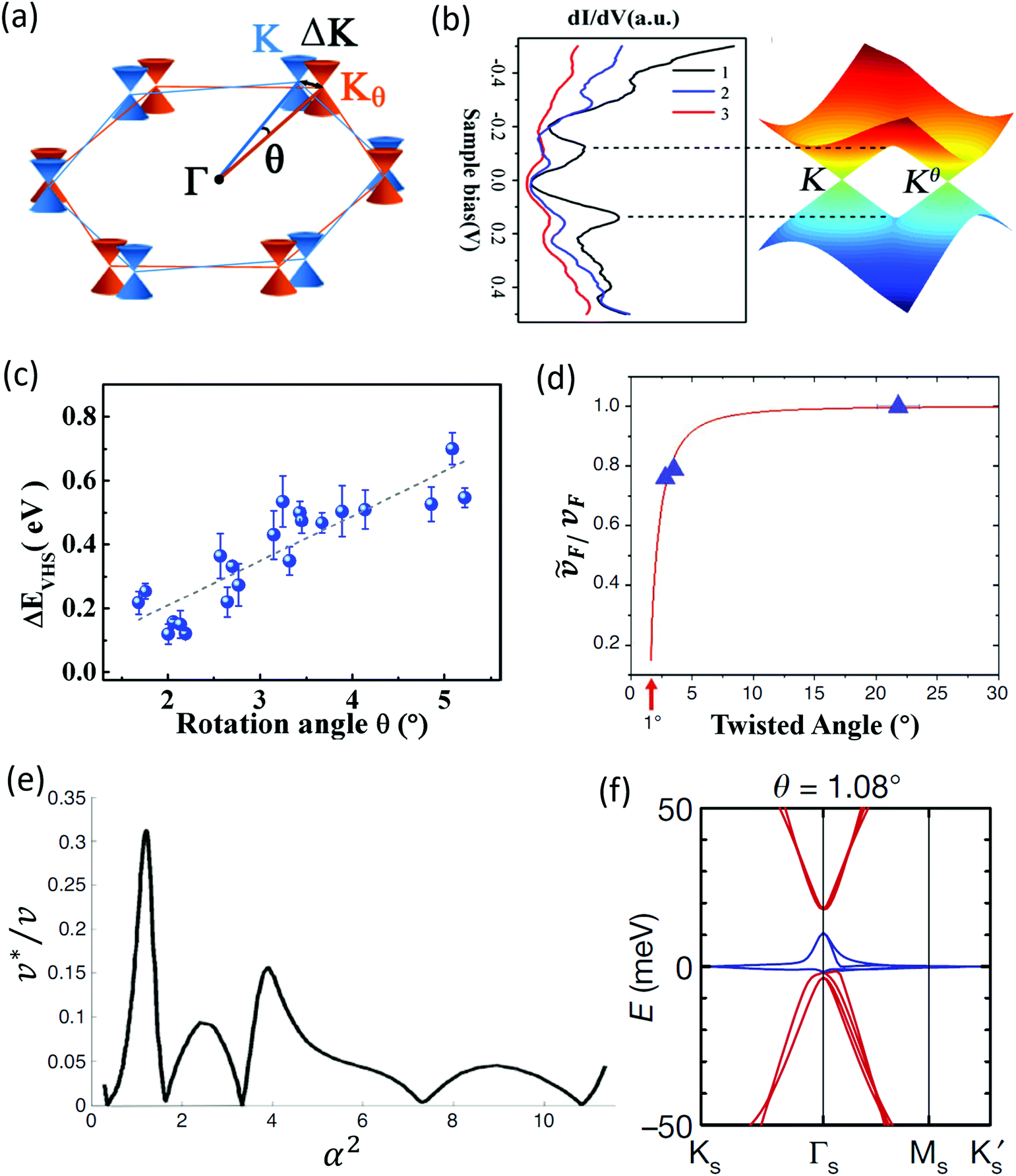 | ||
| Fig. 4 (a) Schematic of the Dirac cones, K and Kθ, of two misoriented graphene layers in the reciprocal space. (b) Left: Tunneling spectra recorded at different positions of a moiré pattern. Right: Electronic band structure of the TBG with a finite interlayer coupling. (c) Angle-dependent VHSs in twisted graphene bilayers. Solid blue circles: average experimental data measured in different twisted graphene bilayers. The gray dotted line: linear fit of the experimental data. (d) Renormalized Fermi velocity as a function of twist angle obtained from Landau-level spectroscopy (symbols) compared to a theoretical simulation (solid line). (e) Renormalized Fermi velocity, v* = vF(1 − 3α2)/(1 + 6α2), as a function of twist angle in the range of 0.18° < θ < 1.2° shows a sequence of magic twist angles at which the Fermi velocity vanishes. (f) The band structure of MATBG shows the formation of flat bands (blue lines) when approaching the magic angle. Figure adapted with permission from: (a and c) ref. 86 Copyright 2014, American Physical Society; (b) ref. 75 Copyright 2012, American Physical Society; (d) ref. 89 Copyright 2011, American Physical Society; (e) ref. 73 Copyright 2011, National Academy of Sciences; (f) ref. 30 Copyright 2018, Springer Nature Limited. | ||
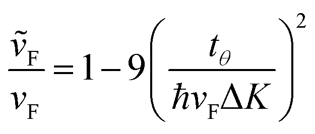
Additionally, the experiments also proved that the low-energy region of the TBG has an angle-dependent Fermi velocity.89,90 When the twist angle is not very small (θ > 3°), the Fermi velocity can be renormalized, and the relationship is as follows:71–73,91
 | (7) |
sin(θ/2) as defined in the above text. The calculation results show that the bandwidth of flat bands in magic-angle TBG is approximately 12 meV (E > 0) or 2 meV (E < 0). The flat band of the MATBG was measured experimentally for the first time in 2015, and the corresponding magic angle was about 1.11°.92
 | (8) |
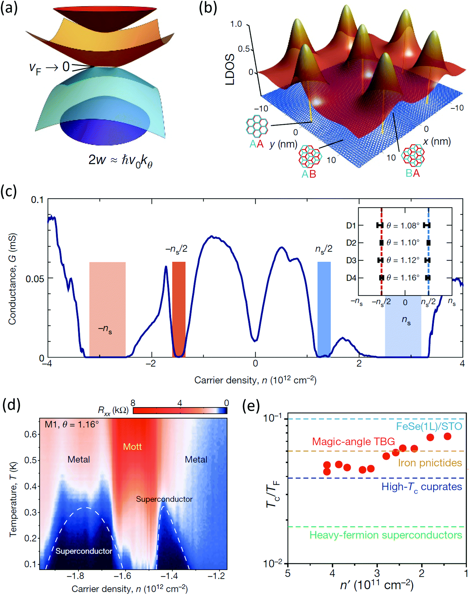 | ||
| Fig. 5 (a) Illustration of the effect of interlayer hybridization for 2w ≈ ħv0k. (b) Spatial distribution diagram of local density of states (LDOS) of electrons calculated for flat bands with E > 0 in the MATBG. The electron density is strongly concentrated in regions with AA stacking order, but it is mostly depleted in AB- and BA-stacked regions. (c) Carrier dependence of conductance in MATBG. (d) Phase diagram showing the carrier density-dependent superconducting critical temperature in the partially filled flat band. There are two dome-shaped superconducting regions (blue) flanking an insulator (red). (e) Density dependence of Tc/TF as a function of doping for MATBG (red filled circles) compared to other strongly correlated systems. Tc: superconducting temperature, TF: Fermi energy. Figure adapted with permission from: (a–c), ref. 30, Springer Nature Ltd; (d and e), ref. 31, Springer Nature Ltd. | ||
The strong correlation effect of electrons is often accompanied by the Mott-like insulator state transition.98 The sample is expected to behave like a metal according to single-particle band energy theory when the band is not fully filled with electrons. However, it actually behaves like an insulator owing to the strong correlation effect of electrons when the energy band is half-filled, which is usually observed in cuprate materials.99–102 Similarly, low-temperature (∼1 K) electrical transport measurements on MATBG revealed interaction-induced correlated insulating states when the flat band is half-filled with electrons, and thus the state near ±ns/2 is called a half-filling insulating state (Fig. 5c). The MATBG system exhibits two pronounced superconducting domes on each side of the half-filling correlated insulating state when using gate voltage to continuously tune the carrier concentration of the system, with the currently obtained highest superconducting transition temperature of 1.7 K (Fig. 5d), whereas the MATBG system exhibits a quantum anomalous Hall effect (QAHE) at 3/4 filling of the conduction miniband. The QAHE combines topology and magnetism to produce precisely quantized Hall resistance at zero magnetic field. The effect is driven by the spontaneous valley polarization in valley resolved moiré bands with an opposite Chern number.103–106 In recent papers, the researchers observed emergent ferromagnetic hysteresis, reflecting a topological state with Chern number C = 1 that is an orbital ferromagnet. Moreover, the magnetic order of chiral edge states of opposite polarization can be reversed by applying a small direct current, which may have potential applications such as an electrically rewritable magnetic memory.107,108
In MATBG, the ratio of the superconducting transition temperature to Fermi temperature, Tc/TF ≈ 0.1, exceeds the range in which the weak coupling theory of superconductivity can be used, and is similar to Tc/TF in other materials (Fig. 5e) that exhibit superconductivity close to metal–insulator phase transitions. Very recently, nematicity has been observed across the entire superconducting dome of TBG, which indicates that nematic fluctuations might play an important role in the low-temperature phases of MATBG.109 The phenomenology of MATBG is very similar to the phase-diagram of cuprate and pnictide110,111 superconductors in which superconducting domes flank Mott-like insulating phases. Moreover, it is much easier to characterize and control the MATBG than a high-temperature cuprate superconducting system. Therefore, in-depth research on MATBG is expected to help solve the high-temperature superconducting mechanism that has been troubling physicists for more than thirty years.
However, there are still a lot of efforts required to confirm the resemblance between the phenomenology of MATBG and high-temperature superconductors. For example, the parent material of the high-temperature cuprate superconducting system is an anti-ferromagnetic Mott insulator. Current experiments have confirmed that the MATBG is an insulator when the flat band is half-filled, but there is no definite evidence of whether it is a Mott insulator. Moreover, it is needed to be further studied whether the MATBG has anti-ferromagnetism if Mott-like insulator states are confirmed in it. Besides, we still do not know the superconducting pairing mechanism in the MATBG. Apart from this, it is unclear whether there is a pseudogap. On the other hand, there are many problems in the MATBG superconductivity needing to be settled. For example, it is still not clear how the superconductivity in MATBG changes along with angles near the magic angle under the same filling conditions. It is also indefinite whether there is a smaller magic-angle at which similar superconductivity phenomena can occur. In each moiré pattern of the TBG, the stacking order undergoes a change from AB stacking to BA stacking and there are topologically protected boundary states on the AB–BA stacking domain boundary,112,113 which can intrigue an interesting question of how do the superconducting and topological boundary state networks in the MATBG interact with and affect each other. Nevertheless, we hold optimistic opinions about more “magic” properties in the MATBG in the foreseeable future.
3. Moiré excitons in TMD heterobilayers
Transition metal dichalcogenides are another class of materials that attract people's attention apart from graphene because they are natural semiconductor materials with considerable band gaps. Similar to graphene, strong intralayer covalent bonding and weak interlayer vdW interactions make it possible to exfoliate the thin 2D material from its bulk counterpart. Moreover, TMDs display unique semiconducting properties which render them optically active. The anomalous phenomena in graphene-based moiré superlattices attract the interest of researchers to investigate twisted bilayer TMD superlattices. A TMD moiré superlattice is produced when two layers with lattice mismatch are grown on top of one another, naturally endowing them with a nanoscale moiré pattern, which can significantly modify the electronic and optical properties of TMD heterobilayers. In this section, we mainly present the contemporary experimental and theoretical understanding of the unique effects of a moiré superlattice on the interlayer exciton potential landscape and optical properties.3.1 Theory of interlayer exciton moiré potential energy
Various TMD heterobilayers have a type II band alignment where electrons (holes) have lower energies in different layers.37,114,115 The excitons composed of electrons and holes located at different layers through strong Coulombic interactions are referred to as interlayer excitons, shown as violet circles in Fig. 6a,116–118 whereas intralayer excitons are shown as blue and red circles, which were formed by electrons and holes coming from individual layers. Fig. 6b shows the excitation, charge separation and emission processes of interlayer and intralayer excitons. The photoluminescence spectra expected from the heterostructure are shown in Fig. 6c. The blue (X) and red (Y) photoluminescence peaks correspond to pristine intralayer excitons, whereas the violet (I) peaks are from interlayer excitons.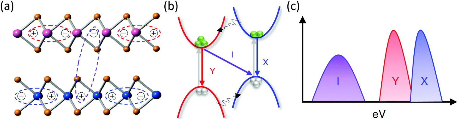 | ||
| Fig. 6 Type II alignment of 2D heterostructures with interlayer interaction strength. (a) Populations of intralayer and interlayer excitons. (b) Excitation, charge separation and emission processes in simplified band pictures. (c) Photoluminescence spectra expected from the heterostructure. Figure adapted with permission from: (a–c), ref. 116 Copyright 2020, Springer Nature Limited. | ||
The moiré pattern in TMD superlattices induced by the lattice mismatch or crystal orientation misalignment can cause modulations in the electronic band structure and optical properties, such as a spatially dependent band gap119 or twist-controlled interlayer excitons.41–43,120 Consider a moiré superlattice of the common chalcogen TMD bilayer WX2/MoX2 (X = Se, S) with a small twist angle θ and an in-plane displacement d, which has two distinct stacking orders of AA stacking (Fig. 7a) and AB stacking (Fig. 7d). This heterojunction has a small lattice mismatch (∼0.1%) and the metal heteroatoms of adjacent layers overlap each other only for periodic moiré periodicities, and thus the wavelength of the moiré superlattice aM can be simplified as aM = a0/θ, in which a0 is the lattice constant of a monolayer TMD. aM (∼18.3 nm) is much larger than the exciton Bohr radius (∼1.3 nm) when the twist angle is smaller than 1°. Therefore, the exciton energy can be approximated by following the local band gap.
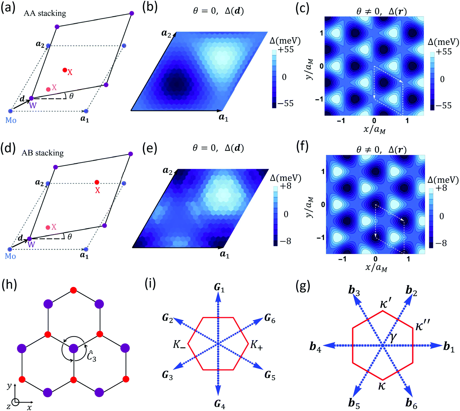 | ||
| Fig. 7 (a) Illustration of an AA stacked WS2/MoS2 heterobilayer with a small twist angle θ and an in-plane displacement d. The variation as a function of displacement d (b) and position r (c) of the interlayer band gap (Δ) within a WS2/MoS2 heterobilayer for AA stacking. (d–f) The same plots as those in (a–c) but for the WS2/MoS2 heterobilayer in AB stacking. (h) Ĉ3 transformation of the TMD lattice. Black arrows denote the phase change by Ĉ3. (i) First-shell reciprocal lattice vectors Gj of a monolayer TMD triangular lattice and the corresponding Brillouin zone (red hexagon). (g) Moiré reciprocal lattice vectors bj and the corresponding Brillouin zone. Figure adapted with permission from: (a, d, i and g) ref. 39, Copyright 2017, American Physical Society; (b, c, e and f) ref. 38, Copyright 2018, American Physical Society. | ||
In this system, the moiré potential modulated interlayer exciton energy is Eg − Eb, where Eg is the band gap between the conduction band minimum (CBM) of MoX2 and the valence band maximum (VBM) of WX2 at the K point, and Eb is the exciton binding energy. The variation of Eb in the moiré pattern is usually neglected, since it is typically smaller than the variation of Eg. According to the ab initio continuum model, the electronic properties calculated from the untwisted reference stackings can be leveraged to approximate the twisted bilayer with a smoothly varying field over the moiré pattern, which can accurately capture atomic relaxations and electronic phenomena.38,39,63,121–124 The procedures for the calculation of excitons’ moiré potential energy in TMD heterobilayers by using the ab initio continuum model are as follows.38
Firstly, calculate the density functional theory (DFT) band structure of untwisted reference cells. Obtain Eg as a periodic function of relative displacement d at the zero-twist angle from the DFT band structure (Fig. 7b and e). The bandgap Eg is defined as the energy difference between the conduction band minimum (CBM) of MoX2 and the valence band maximum (VBM) of WX2 at the K point.
Secondly, obtain the band structure at different local stackings. Since the potential is a smooth periodic function of d in both AA and AB stackings, it can be approximated as 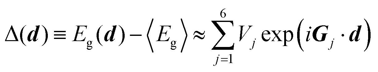 , in which 〈Eg〉 is the average of Eg over d, Gj is one of the first-shell reciprocal lattice vectors (Fig. 7i), and Vj is the moiré potential parameter, denoting the coupling strength between MoX2 and WX2 in TMD heterobilayers. Moreover, the existence of threefold rotational symmetry (Ĉ3) in each TMD layer leads to V1 = V3 = V5, V2 = V4 = V6 (Fig. 7h). Therefore, Δ(d) is always real.
Finally, approximate the interlayer Bloch-wave coupling over a single moiré supercell. Assume that, in a moiré supercell, the variation of Eg locally follows 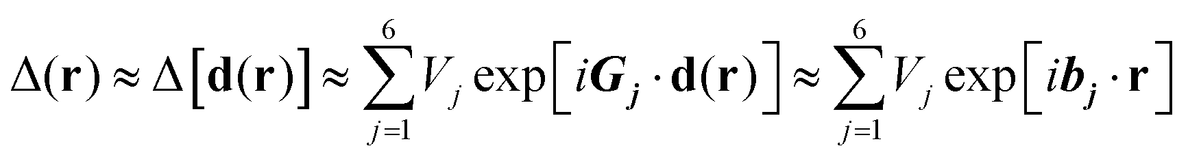 (Fig. 7c and f), where the local configuration, d, is a function of space, d(r), and bj = θGj × ẑ is the reciprocal lattice vector of the moiré pattern (Fig. 7g).
Therefore, the moiré pattern formed in the twisted TMD heterobilayer can lead to a position-dependent potential for excitons across a single moiré supercell, with spatial modulation up to ∼150 meV for interlayer excitons in the MoS2/WSe2 heterobilayer with rotational alignment and lattice mismatch, which has been experimentally identified by STM/STS (Fig. 8a and b).119 Additionally, TMDs are highly sensitive to crystal structure symmetry and interlayer coupling, which makes them highly susceptible to stacking orders. Atoms stacked in different configurations are known as atomic registries, which can cause valence and conduction bands to possess different energies, giving additional control over the electronic and optical properties in these systems.125–129
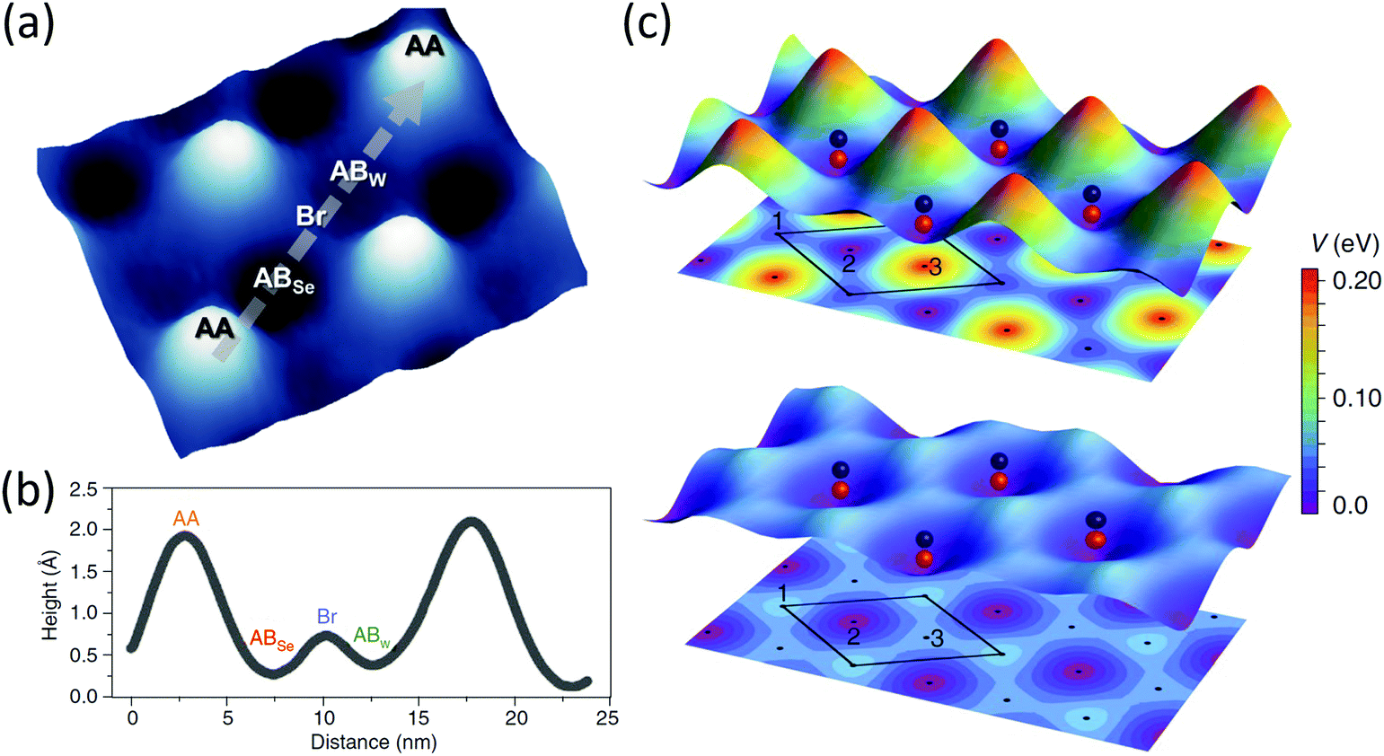 | ||
| Fig. 8 (a) STM measurement of the topographic height across a single moiré supercell of the MoS2/WSe2 moiré pattern. (b) A height profile along the diagonal line from AA to AA in a moiré supercell (arrow in a). (c) Illustration of the 2D K valley moiré potentials in both 3D graphs and 2D projections that can trap long-lived interlayer excitons (red and black spheres) in the local minima as they move from one location to another. 1, 2 and 3 indicate high symmetry points in a TMD heterobilayer of WS2/WSe2 with a twist angle of 0° (top) and 60° (bottom). Figure adapted with permission from: (a and b) ref. 119 Copyright 2017, AAAS; (c) ref. 130 Copyright 2020, Springer Nature Limited. | ||
For interlayer excitons in a moiré pattern, the theory predicts that the moiré potential generally results in localized exciton states near the potential minimum positions. Fig. 8c shows that the depth of moiré potential for 0° is much larger than that for 60°. It implies that the moiré pattern leads to twist-angle-dependent periodic potential landscapes that govern the transport and relaxation of interlayer excitons, which has been experimentally confirmed.130 The existence of moiré potential in twisted TMD heterobilayers suggests a vdW heterostructure based strategy for realizing two-dimensional nanoscale arrays of uniform quantum dots, which has a great prospect for application in quantum photonic devices. Yu et al.40 studied interlayer excitons in the MoX2/WX2 heterobilayer and found that they have a unique spin-dependent hopping, which can be switched off when applying a perpendicular electric field according to DFT calculations, giving the possibility to turn the superlattices into identical arrays of nanodots that act as uniform quantum emitters. Besides, the spin optical selection rules can be flipped by switching the positions of emitters in the moiré due to the electric field. These properties of moiré excitons in TMD heterobilayers suggest the feasibility of engineering artificial excitonic crystals for nanophotonics and quantum information applications.131
3.2 Twist-dependent moiré excitons in TMD heterobilayers
Although the theory of exciton potential energy in twisted TMD heterobilayers has predicted notable effects of the moiré potential on interlayer excitons years before,38,40,120 the impacts of the moiré potential on light emission and absorption in heterobilayers of TMDs have not been detected experimentally until 2019. It was found that interlayer excitons have a valley degree of freedom, and different interlayer excitons at a given valley can absorb light with different circular polarization; besides, the excitons interact with light of a specific polarization that depends on the local symmetry of the atoms arranged periodically in the heterobilayer.41–44Recently, the WSe2/WS2 moiré superlattice system with different twist angles was studied experimentally. Jin et al.42 measured the PL of the WSe2/WS2 heterobilayer and found that there is no monolayer PL in the heterostructure, which indicates the existence of strong interlayer coupling. Three peaks emerge around the original A exciton resonance of WSe2 in the reflection spectrum in the small twisted WSe2/WS2 moiré superlattice, corresponding to distinct moiré exciton states, whereas, in the superlattice with a large twist angle, it shows only a single resonance in energy near the A exciton of WSe2 (Fig. 9a). These phenomena can be explained with a theoretical model in which the moiré potential is much stronger than the kinetic energy of exciton, generating multiple flat exciton minibands.
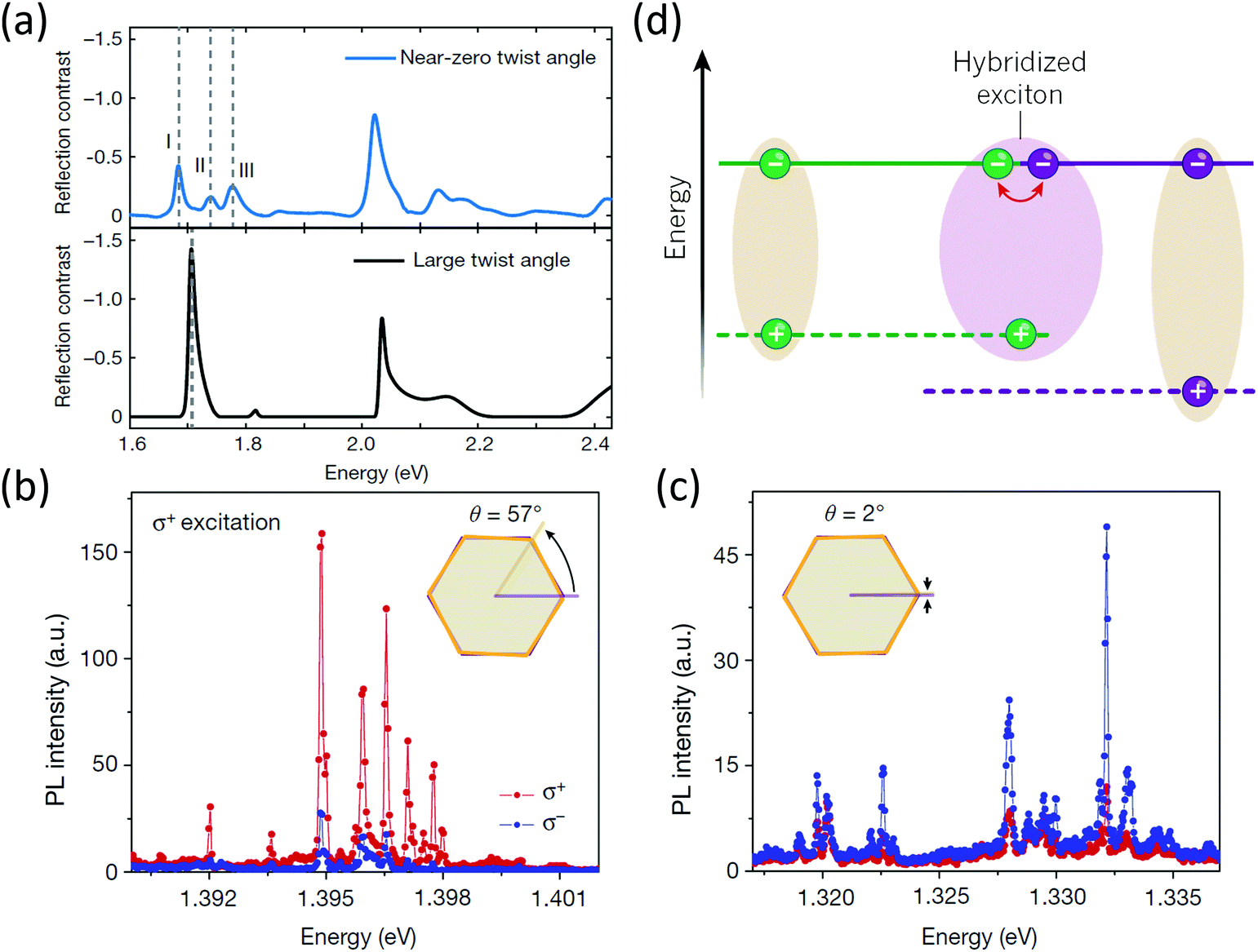 | ||
| Fig. 9 (a) Reflection contrast spectrum of a small twisted WSe2/WS2 heterostructure (light blue, top) compared to that of a WSe2/WS2 heterostructure with a large twist angle (black, bottom). Helicity-resolved PL spectra of trapped interlayer excitons of MoSe2/WSe2 heterobilayers with twist angles of 57° (b) and 2° (c). The insets illustrate the twist angles of the two samples. (d) The band diagram showing intralayer excitons can be hybridized with interlayer excitons in heterobilayers of MoSe2/WS2 (indicated in purple). Figure adapted with permission from: (a) ref. 42 Copyright 2019, Springer Nature Limited; (b and c) ref. 43 Copyright 2019, Springer Nature Limited; (d) ref. 132 Copyright 2019, Springer Nature Limited. | ||
Seyler et al. studied individual interlayer excitons trapped in the moiré potential in the MoSe2/WSe2 moiré superlattice with a small twist angle.43 They found that there are several narrow peaks near the free interlayer exciton energy at extremely low temperatures when using a low excitation power. The linewidth of peaks is about 110 μeV, making it comparable with quantum emitters. However, the excitons can delocalize with broadened linewidth emissions under high power excitation. Besides, the trapped interlayer excitons exhibit strong circular polarization of the same helicity for a given twist angle (Fig. 9b and c). The samples are excited with σ+-polarized light at 1.72 eV. The σ+ and σ− components of the photoluminescence are shown in red and blue, respectively. The PL from the heterobilayer with a twist angle of 57° is co-circularly polarized, but that from the heterobilayer with a twist angle of 2° is cross-circularly polarized. This phenomenon suggests that the moiré-defined trapping sites preserve Ĉ3 symmetry. Therefore, the observation of narrow interlayer PL lines verified the existence of moiré potential with inherited valley-contrasting physics, trapping the interlayer excitons.
The experimental result of Tran et al. is the observation of multiple interlayer exciton resonances with circularly polarized emission in the same moiré superlattice system, a MoSe2/WSe2 heterobilayer with a small twist angle.41 They can locate the emission peaks of interlayer excitons and determine the extent of energy separation between peaks dependent on twist angle in the moiré superlattice. This result provides an exciting opportunity for high-performance semiconductor lasers, quantum emitter arrays and a platform for studying exotic quantum phases.
Additionally, the research also reveals that intralayer excitons can hybridize with interlayer excitons in MoSe2/WS2 owing to the conduction band delocalized over both layers, which leads to a resonant enhancement of moiré superlattice effects.44 The essence of hybridization between intralayer and interlayer excitons is that the conduction band edges of MoSe2 and WS2 are near-degeneracy (Fig. 9d), which can amplify the impact of the moiré potential on the optical features of these heterobilayers. The energy of hybridized excitons relies on the interlayer twist angle because hybridized excitons are formed by holes that reside in MoSe2 binding to a twist-dependent superposition of electron states in the adjacent monolayers, which gives an additional degree of freedom to modulate the optical properties of TMD heterojunctions.
The above four studies all studied the impact of the moiré superlattice on the optical properties of moiré excitons in TMD heterobilayers with different twist angles experimentally and found many novel phenomena. The origin of the observed effects is interlayer excitons trapped in a smooth moiré potential with inherited valley-contrasting physics. However, these studies are only the first footstep toward complete understanding of and control over individual moiré potentials. In-depth knowledge of the scale and depth of potentials is expected to provide control over single exciton traps, which provides opportunities for obtaining quantum emitter arrays of versatile tunability in twisted TMD heterostructures.
4. Conclusion and perspective
In this paper, we have mainly reviewed quantum phenomena in two-dimensional heterostructures. The electronic and optical properties of graphene-based and TMD-based heterojunctions have been summarized, and the physical mechanism of quantum phenomena and the moiré potential in moiré superlattices have been elaborated. The moiré superlattice modulated properties in 2D materials have been studied at a remarkable level for a wide variety of materials, among graphene/h-BN, (magic-angle) twisted graphene bilayers and TMD heterobilayers. In graphene/h-BN heterostructures, the moiré superlattice can strongly modify the Dirac spectrum and assist optical spectroscopy in the fractional quantum Hall regime, which results in superlattice minibands and leads to Hofstadter-butterfly spectra under a strong magnetic field, whereas in twisted graphene bilayers its effects are enhanced by interlayer resonant conditions, resulting in a superconductor–insulator transition at magic twist angles. Moreover, in TMD heterobilayers, the appearance of the moiré superlattice is accompanied by the twist angle-dependent periodic potential landscape that can trap interlayer excitons near the potential minima, resulting in anomalous optical phenomena. Although lots of intriguing physical phenomena have been observed experimentally, exploiting the distinct advantages of the angle-dependent moiré superlattice in 2D materials and their superior devices is still full of challenges. In perspective, we propose several research directions for 2D material-based vdW-coupled twistronic materials of great importance, which are worth being discussed thoroughly in the future.(1) Precise control of twist angle
vdW moiré heterostructures can be fabricated by using a variety of methods, including CVD epitaxial growth, monolayer folding and tear-and-stack methods. Each method has its advantages and disadvantages, but the issue of common concern is how to precisely control the twist angle, which is also the most important obstacle to immediate progress in understanding the properties of 2D twistronic materials. Uncontrolled strains related to details of how mechanical contact is established between the twisted layers can strongly influence the physical properties, such as basic features of the phase diagram that express gapped states, the appearance or absence of superconductivity and orbital magnetism in the MATBG.(2) Physical mechanism of superconductivity in the MATBG
Two strongly correlated quantum states have been observed in the MATBG due to the enhanced interlayer coupling compared with graphene/h-BN heterostructures. However, there are some important problems that remain to be solved. For example, there is no definite evidence whether the MATBG is a Mott insulator when the flat band is half-filled; moreover, it is needed to be further studied whether the MATBG has anti-ferromagnetism if a Mott-like insulator state is confirmed in it. Besides, we are not yet clear on the superconducting pairing mechanism in the MATBG. The resemblance between the phenomenology of high-temperature superconductors and MATBG is striking, but whether these similarities reflect a deep connection remains to be seen.(3) Development of multi-functional twistronic devices
TMD twistronic materials are a big family with rapid development and innovation. In twisted TMD heterobilayers, the moiré potential generally results in localized exciton states near the potential minimum position, which suggests a vdW heterostructure based strategy for realizing 2D periodic arrays that act as tunable uniform quantum light emitters. Furthermore, the number of trapped excitons could go down to one by carefully tuning the size and depth of the moiré potential, offering a source of single-photon emitter arrays. In addition, interlayer excitons at a given valley can absorb light with different circular polarization, which provides the possibility to fabricate high-performance semiconductor lasers and entangled photon sources as well as artificial excitonic crystals.In conclusion, the moiré superlattice in 2D materials provides a platform of versatile tunability for studying exotic quantum phases of matter with imaging possibilities. Progress is being made in this direction, and we can expect that studies of moiré superlattices can advance twistronics physics and help us understand other condensed matter systems.
Conflicts of interest
The authors declare no conflicts of interest.Acknowledgements
This work was supported by the National Key Research and Development Program of China (2019YFA0210203), Beijing Natural Science Foundation (Z180011), the National Science Foundation of China (21790364, 12027807, and 61521004), China Postdoctoral Science Foundation (2019M660283), and the High-Performance Computing Platform of Peking University.References
- A. K. Geim and I. V. Grigorieva, van der Waals heterostructures, Nature, 2013, 499, 419–425 CrossRef CAS PubMed
.
- K. S. Novoselov, A. Mishchenko, A. Carvalho and A. H. C. Neto, 2D materials and van der Waals heterostructures, Science, 2016, 353(6298), aac9439 CrossRef CAS PubMed
- R. Wang, F. Zhou, L. Lv, S. Zhou, Y. Yu, F. Zhuge, H. Li, L. Gan and T. Zhai, Modulation of the anisotropic electronic properties in ReS2 via ferroelectric film, CCS Chem., 2019, 1, 268–277 CAS
- F. Z. Wang, Z. Y. Wang, W. D. Sun, Z. B. Wang, Y. M. Bai, T. Hayat, A. Alsaedi and Z. A. Tan, High Performance quasi-2D perovskite sky-blue light-emitting diodes using a dual-ligand strategy, Small, 2020, 16(32) DOI:10.1002/smll.202002940
- A. Pandey, R. Yadav, M. Kaur, P. Singh, A. Gupta and S. Husale, High performing flexible optoelectronic devices using thin films of topological insulator, Sci. Rep., 2021, 11(1) DOI:10.1038/s41598-020-80738-8
- E. C. Nelson, N. L. Dias, K. P. Bassett, S. N. Dunham, V. Verma, M. Miyake, P. Wiltzius, J. A. Rogers, J. J. Coleman and X. L. Li,
et al., Epitaxial growth of three-dimensionally architectured optoelectronic devices, Nat. Mater., 2011, 10, 676–681 CrossRef CAS PubMed
- B. W. H. Baugher, H. O. H. Churchill, Y. F. Yang and P. Jarillo-Herrero, Optoelectronic devices based on electrically tunable p–n diodes in a monolayer dichalcogenide, Nat. Nanotechnol., 2014, 9, 262–267 CrossRef CAS PubMed
- M. M. Islam, D. Dev, A. Krishnaprasad, L. Tetard and T. Roy, Optoelectronic synapse using monolayer MoS2 field effect transistors, Sci. Rep., 2020, 10(1), 21870 CrossRef CAS PubMed
- A. A. Puretzky, L. B. Liang, X. F. Li, K. Xiao, B. G. Sumpter, V. Meunier and D. B. Geohegan, Twisted MoSe2 bilayers with variable local stacking and interlayer coupling revealed by low-frequency Raman spectroscopy, ACS Nano, 2016, 10, 2736–2744 CrossRef CAS PubMed
- W. T. Geng, V. Wang, Y. C. Liu, T. Ohno and J. Nara, Moire potential, lattice corrugation, and band gap spatial variation in a twist-free MoTe2/MoS2 heterobilayer, J. Phys. Chem. Lett., 2020, 11, 2637–2646 CrossRef CAS PubMed
- S. X. Huang, L. B. Liang, X. Ling, A. A. Puretzky, D. B. Geohegan, B. G. Sumpter, J. Kong, V. Meunier and M. S. Dresselhaus, Low-frequency interlayer Raman modes to probe interface of twisted bilayer MoS2, Nano Lett., 2016, 16, 1435–1444 CrossRef CAS PubMed
- K. Wang, B. Huang, M. Tian, F. Ceballos, M. W. Lin, M. Mahjouri-Samani, A. Boulesbaa, A. A. Puretzky, C. M. Rouleau and M. Yoon,
et al., Interlayer coupling in twisted WSe2/WS2 bilayer heterostructures revealed by optical spectroscopy, ACS Nano, 2016, 10, 6612–6622 CrossRef CAS PubMed
- B. Hunt, J. D. Sanchez-Yamagishi, A. F. Young, M. Yankowitz, B. J. LeRoy, K. Watanabe, T. Taniguchi, P. Moon, M. Koshino and P. Jarillo-Herrero,
et al., Massive Dirac fermions and Hofstadter butterfly in a van der Waals heterostructure, Science, 2013, 340, 1427–1430 CrossRef CAS PubMed
- C. R. Dean, L. Wang, P. Maher, C. Forsythe, F. Ghahari, Y. Gao, J. Katoch, M. Ishigami, P. Moon and M. Koshino,
et al., Hofstadter's butterfly and the fractal quantum Hall effect
in moire superlattices, Nature, 2013, 497, 598–602 CrossRef CAS PubMed
- L. A. Ponomarenko, R. V. Gorbachev, G. L. Yu, D. C. Elias, R. Jalil, A. A. Patel, A. Mishchenko, A. S. Mayorov, C. R. Woods and J. R. Wallbank,
et al., Cloning of Dirac fermions in graphene superlattices, Nature, 2013, 497, 594–597 CrossRef CAS PubMed
- M. Yankowitz, J. M. Xue, D. Cormode, J. D. Sanchez-Yamagishi, K. Watanabe, T. Taniguchi, P. Jarillo-Herrero, P. Jacquod and B. J. LeRoy, Emergence of superlattice Dirac points in graphene on hexagonal boron nitride, Nat. Phys., 2012, 8, 382–386 Search PubMed
- W. Yang, G. R. Chen, Z. W. Shi, C. C. Liu, L. C. Zhang, G. B. Xie, M. Cheng, D. M. Wang, R. Yang and D. X. Shi,
et al., Epitaxial growth of single-domain graphene on hexagonal boron nitride, Nat. Mater., 2013, 12, 792–797 CrossRef CAS PubMed
- L. Wang, Y. D. Gao, B. Wen, Z. Han, T. Taniguchi, K. Watanabe, M. Koshino, J. Hone and C. R. Dean, Evidence for a fractional fractal quantum Hall effect in graphene superlattices, Science, 2015, 350, 1231–1234 CrossRef CAS PubMed
- L. X. Liu and T. Y. Zhai, Wafer-scale vertical van der Waals heterostructures, Infomat, 2021, 3, 3–21 CrossRef CAS
- C. R. Dean, A. F. Young, I. Meric, C. Lee, L. Wang, S. Sorgenfrei, K. Watanabe, T. Taniguchi, P. Kim and K. L. Shepard,
et al., Boron nitride substrates for high-quality graphene electronics, Nat. Nanotechnol., 2010, 5, 722–726 CrossRef CAS PubMed
- J. M. Xue, J. Sanchez-Yamagishi, D. Bulmash, P. Jacquod, A. Deshpande, K. Watanabe, T. Taniguchi, P. Jarillo-Herrero and B. J. Leroy, Scanning tunnelling microscopy and spectroscopy of ultra-flat graphene on hexagonal boron nitride, Nat. Mater., 2011, 10, 282–285 CrossRef CAS PubMed
- G. Giovannetti, P. A. Khomyakov, G. Brocks, P. J. Kelly and J. van den Brink, Substrate-induced band gap in graphene on hexagonal boron nitride: Ab initio density functional calculations, Phys. Rev. B: Condens. Matter Mater. Phys., 2007, 76, 073103 CrossRef
- F. Amet, J. R. Williams, K. Watanabe, T. Taniguchi and D. Goldhaber-Gordon, Insulating behavior at the neutrality point in single-layer graphene, Phys. Rev. Lett., 2013, 110(21), 216601 CrossRef CAS PubMed
- R. V. Gorbachev, J. C. W. Song, G. L. Yu, A. V. Kretinin, F. Withers, Y. Cao, A. Mishchenko, I. V. Grigorieva, K. S. Novoselov and L. S. Levitov,
et al., Detecting topological currents in graphene superlattices, Science, 2014, 346, 448–451 CrossRef CAS PubMed
- C. R. Woods, L. Britnell, A. Eckmann, R. S. Ma, J. C. Lu, H. M. Guo, X. Lin, G. L. Yu, Y. Cao and R. V. Gorbachev,
et al., Commensurate-incommensurate transition in graphene on hexagonal boron nitride, Nat. Phys., 2014, 10, 451–456 Search PubMed
- C. H. Park, L. Yang, Y. W. Son, M. L. Cohen and S. G. Louie, Anisotropic behaviours of massless Dirac fermions in graphene under periodic potentials, Nat. Phys., 2008, 4, 213–217 Search PubMed
- C. H. Park, L. Yang, Y. W. Son, M. L. Cohen and S. G. Louie, New generation of massless Dirac fermions in graphene under external periodic potentials, Phys. Rev. Lett., 2008, 101(12), 126804 CrossRef PubMed
- G. L. Yu, R. V. Gorbachev, J. S. Tu, A. V. Kretinin, Y. Cao, R. Jalil, F. Withers, L. A. Ponomarenko, B. A. Piot and M. Potemski,
et al., Hierarchy of Hofstadter states and replica quantum Hall ferromagnetism in graphene superlattices, Nat. Phys., 2014, 10, 525 Search PubMed
- G. H. Li, A. Luican, J. M. B. L. dos Santos, A. H. Castro Neto, A. Reina, J. Kong and E. Y. Andrei, Observation of Van Hove singularities in twisted graphene layers, Nat. Phys., 2010, 6, 109–113 Search PubMed
- Y. Cao, V. Fatemi, A. Demir, S. Fang, S. L. Tomarken, J. Y. Luo, J. D. Sanchez-Yamagishi, K. Watanabe, T. Taniguchi and E. Kaxiras,
et al., Correlated insulator behaviour at half-filling in magic-angle graphene superlattices, Nature, 2018, 556, 80–84 CrossRef CAS PubMed
- Y. Cao, V. Fatemi, S. Fang, K. Watanabe, T. Taniguchi, E. Kaxiras and P. Jarillo-Herrero, Unconventional superconductivity in magic-angle graphene superlattices, Nature, 2018, 556, 43–50 CrossRef CAS PubMed
- K. F. Mak and J. Shan, Photonics and optoelectronics of 2D semiconductor transition metal dichalcogenides, Nat. Photonics, 2016, 10, 216–226 CrossRef CAS
- D. Unuchek, A. Ciarrocchi, A. Avsar, K. Watanabe, T. Taniguchi and A. Kis, Room-temperature electrical control of exciton flux in a van der Waals heterostructure, Nature, 2018, 560, 340–344 CrossRef CAS PubMed
- P. F. Qi, Y. Luo, W. Li, Y. Cheng, H. Y. Shan, X. L. Wang, Z. Liu, P. M. Ajayan, J. Lou and Y. L. Hou,
et al., Remote lightening and ultrafast transition: intrinsic modulation of exciton spatiotemporal dynamics in monolayer MoS2, ACS Nano, 2020, 14, 6897–6905 CrossRef CAS PubMed
- J. Kang, S. Tongay, J. Zhou, J. B. Li and J. Q. Wu, Band offsets and heterostructures of two-dimensional semiconductors, Appl. Phys. Lett., 2013, 102(1), 666 CrossRef
- K. Kosmider and J. Fernandez-Rossier, Electronic properties of the MoS2-WS2 heterojunction, Phys. Rev. B: Condens. Matter Mater. Phys., 2013, 87(7) DOI:10.1103/PhysRevB.87.075451
- M. H. Chiu, C. D. Zhang, H. W. Shiu, C. P. Chuu, C. H. Chen, C. Y. S. Chang, C. H. Chen, M. Y. Chou, C. K. Shih and L. J. Li, Determination of band alignment in the single-layer MoS2/WSe2 heterojunction, Nat. Commun., 2015, 6(1), 7666 CrossRef CAS PubMed
- F. C. Wu, T. Lovorn and A. H. MacDonald, Theory of optical absorption by interlayer excitons in transition metal dichalcogenide heterobilayers, Phys. Rev. B, 2018, 97(3), 035306 CrossRef CAS
- F. C. Wu, T. Lovorn and A. H. MacDonald, Topological exciton bands in moire heterojunctions, Phys. Rev. Lett., 2016, 118(14), 147401 CrossRef PubMed
- H. Y. Yu, G. B. Liu, J. J. Tang, X. D. Xu and W. Yao, Moire excitons: From programmable quantum emitter arrays to spin–orbit-coupled artificial lattices, Sci. Adv., 2017, 3(11), e1701696 CrossRef PubMed
- K. Tran, G. Moody, F. C. Wu, X. B. Lu, J. Choi, K. Kim, A. Rai, D. A. Sanchez, J. M. Quan and A. Singh,
et al., Evidence for moire excitons in van der Waals heterostructures, Nature, 2019, 567, 71–75 CrossRef CAS PubMed
- C. H. Jin, E. C. Regan, A. M. Yan, M. I. B. Utama, D. Q. Wang, S. H. Zhao, Y. Qin, S. J. Yang, Z. R. Zheng and S. Y. Shi,
et al., Observation of moire excitons in WSe2/WS2 heterostructure superlattices, Nature, 2019, 569, E7 CrossRef CAS PubMed
- K. L. Seyler, P. Rivera, H. Y. Yu, N. P. Wilson, E. L. Ray, D. G. Mandrus, J. Q. Yan, W. Yao and X. D. Xu, Signatures of moire-trapped valley excitons in MoSe2/WSe2 heterobilayers, Nature, 2019, 567, 66–70 CrossRef CAS PubMed
- E. M. Alexeev, D. A. Ruiz-Tijerina, M. Danovich, M. J. Hamer, D. J. Terry, P. K. Nayak, S. Ahn, S. Pak, J. Lee and J. I. Sohn,
et al., Resonantly hybridized excitons in moire superlattices in van der Waals heterostructures, Nature, 2019, 572, E8 CrossRef CAS PubMed
- A. K. Geim and K. S. Novoselov, The rise of graphene, Nat. Mater., 2007, 6, 183–191 CrossRef CAS PubMed
- A. H. Castro Neto, F. Guinea, N. M. R. Peres, K. S. Novoselov and A. K. Geim, The electronic properties of graphene, Rev. Mod. Phys., 2009, 81, 109–162 CrossRef CAS
- A. K. Geim, Graphene: Status and prospects, Science, 2009, 324, 1530–1534 CrossRef CAS PubMed
- B. B. Shi, Y. D. Xiao, T. Y. Han, H. T. Cheng, J. C. Zhang, Q. Jiang, H. L. Peng, H. Zhang, X. Zhu and Z. Y. Fang, Controllable inversion symmetry breaking in single layer graphene induced by sub-lattice contrasted charge polarization, Carbon, 2020, 163, 63–69 CrossRef CAS
- S. Sahoo, Quantum Hall effect in graphene: Status and prospects, Indian J. Pure Appl. Phys., 2011, 49, 367–371 CAS
- V. P. Gusynin and S. G. Sharapov, Unconventional integer quantum Hall effect in graphene, Phys. Rev. Lett., 2005, 95, 146801 CrossRef CAS PubMed
- Y. B. Zhang, Y. W. Tan, H. L. Stormer and P. Kim, Experimental observation of the quantum Hall effect and Berry's phase in graphene, Nature, 2005, 438, 201–204 CrossRef CAS PubMed
- C. R. Dean, A. F. Young, P. Cadden-Zimansky, L. Wang, H. Ren, K. Watanabe, T. Taniguchi, P. Kim, J. Hone and K. L. Shepard, Multicomponent fractional quantum Hall effect in graphene, Nat. Phys., 2011, 7, 693–696 Search PubMed
- K. S. Novoselov, A. K. Geim, S. V. Morozov, D. Jiang, M. I. Katsnelson, I. V. Grigorieva, S. V. Dubonos and A. A. Firsov, Two-dimensional gas of massless Dirac fermions in graphene, Nature, 2005, 438, 197–200 CrossRef CAS PubMed
- Y. Zeng, J. I. A. Li, S. A. Dietrich, O. M. Ghosh, K. Watanabe, T. Taniguch, J. Hone and C. R. Dean, High-quality magnetotransport in graphene using the edge-free corbino geometry, Phys. Rev. Lett., 2019, 122, 13 CrossRef
- M. Yankowitz, Q. Ma, P. Jarillo-Herrero and B. J. LeRoy, van der Waals heterostructures combining graphene and hexagonal boron nitride, Nat. Rev. Phys., 2019, 1, 112–125 CrossRef CAS
- M. Yankowitz, J. Jung, E. Laksono, N. Leconte, B. L. Chittari, K. Watanabe, T. Taniguchi, S. Adam, D. Graf and C. R. Dean, Dynamic band-structure tuning of graphene moire superlattices with pressure, Nature, 2018, 557, 404–408 CrossRef CAS PubMed
- Z. G. Chen, Z. W. Shi, W. Yang, X. B. Lu, Y. Lai, H. G. Yan, F. Wang, G. Y. Zhang and Z. Q. Li, Observation of an intrinsic bandgap and Landau level renormalization in graphene/boron-nitride heterostructures, Nat. Commun., 2014, 5, 4461 CrossRef CAS PubMed
- E. Y. Wang, X. B. Lu, S. J. Ding, W. Yao, M. Z. Yan, G. L. Wan, K. Deng, S. P. Wang, G. R. Chen and L. G. Ma,
et al., Gaps induced by inversion symmetry breaking and second-generation Dirac cones in graphene/hexagonal boron nitride, Nat. Phys., 2016, 12, 1111–1115 Search PubMed
- R. Ribeiro-Palau, C. J. Zhang, K. Watanabe, T. Taniguchi, J. Hone and C. R. Dean, Twistable electronics with dynamically rotatable heterostructures, Science, 2018, 361(6403), 690–693 CrossRef CAS
- H. Kim, N. Leconte, B. L. Chittari, K. Watanabe, T. Taniguchi, A. H. MacDonald, J. Jung and S. Jung, Accurate gap determination in monolayer and bilayer graphene/h-BN moire superlattices, Nano Lett., 2018, 18, 7732–7741 CrossRef CAS PubMed
- M. Yankowitz, K. Watanabe, T. Taniguchi, P. San-Jose and B. J. LeRoy, Pressure-induced commensurate stacking of graphene on boron nitride, Nat. Commun., 2016, 7, 13168 CrossRef CAS PubMed
- J. C. W. Song, A. V. Shytov and L. S. Levitov, Electron interactions and gap opening in graphene superlattices, Phys. Rev. Lett., 2013, 111, 266801 CrossRef PubMed
- J. Jung, A. M. DaSilva, A. H. MacDonald and S. Adam, Origin of band gaps in graphene on hexagonal boron nitride, Nat. Commun., 2015, 6, 6308 CrossRef CAS PubMed
- D. R. Hofstadter, Energy-levels and wave-functions of bloch electrons in rational and irrational magnetic-fields, Phys. Rev. B: Solid State, 1976, 14, 2239–2249 CrossRef CAS
- J. Gonzalez, Kohn–Luttinger superconductivity in graphene, Phys. Rev. B: Condens. Matter Mater. Phys., 2008, 78 DOI:10.1103/PhysRevB.78.205431
- I. Martin and C. D. Batista, Itinerant electron-driven chiral magnetic ordering and spontaneous quantum hall effect in triangular lattice models, Phys. Rev. Lett., 2008, 101(15), 156402 CrossRef PubMed
- R. Nandkishore, L. S. Levitov and A. V. Chubukov, Chiral superconductivity from repulsive interactions in doped graphene, Nat. Phys., 2012, 8, 158–163 Search PubMed
- W. S. Wang, Y. Y. Xiang, Q. H. Wang, F. Wang, F. Yang and D. H. Lee, Functional renormalization group and variational Monte Carlo studies of the electronic instabilities in graphene near 1/4 doping, Phys. Rev. B: Condens. Matter Mater. Phys., 2012, 85(3), 154–159 Search PubMed
- J. Gonzalez, Magnetic and Kohn–Luttinger instabilities near a Van Hove singularity: Monolayer versus twisted bilayer graphene, Phys. Rev. B: Condens. Matter Mater. Phys., 2013, 88(12), 125434 CrossRef
- J. L. McChesney, A. Bostwick, T. Ohta, T. Seyller, K. Horn, J. Gonzalez and E. Rotenberg, Extended van Hove singularity and superconducting instability in doped graphene, Phys. Rev. Lett., 2010, 104, 136803 CrossRef CAS PubMed
- J. M. B. L. dos Santos, N. M. R. Peres and A. H. Castro, Graphene bilayer with a twist: Electronic structure, Phys. Rev. Lett., 2007, 99(25), 256802 CrossRef PubMed
- E. S. Morell, J. D. Correa, P. Vargas, M. Pacheco and Z. Barticevic, Flat bands in slightly twisted bilayer graphene: Tight-binding calculations, Phys. Rev. B: Condens. Matter Mater. Phys., 2010, 82, 121407 CrossRef
- R. Bistritzer and A. H. MacDonald, Moire bands in twisted double-layer graphene, Proc. Natl. Acad. Sci. U. S. A., 2011, 108, 12233–12237 CrossRef CAS PubMed
- L. Vanhove, The occurrence of singularities in the elastic frequency distribution of a crystal, Phys. Rev., 1953, 89, 1189–1193 CrossRef CAS
- W. Yan, M. X. Liu, R. F. Dou, L. Meng, L. Feng, Z. D. Chu, Y. F. Zhang, Z. F. Liu, J. C. Nie and L. He, Angle-dependent van Hove singularities in a slightly twisted graphene bilayer, Phys. Rev. Lett., 2012, 109(12), 126801 CrossRef PubMed
- I. Brihuega, P. Mallet, H. Gonzalez-Herrero, G. T. de Laissardiere, M. M. Ugeda, L. Magaud, J. M. Gomez-Rodriguez, F. Yndurain and J. Y. Veuillen, Unraveling the intrinsic and robust nature of van Hove singularities in twisted bilayer graphene by scanning tunneling microscopy and theoretical analysis, Phys. Rev. Lett., 2012, 109, 196802 CrossRef CAS PubMed
- R. W. Havener, H. L. Zhuang, L. Brown, R. G. Hennig and J. Park, Angle-resolved Raman imaging of inter layer rotations and interactions in twisted bilayer graphene, Nano Lett., 2012, 12, 3162–3167 CrossRef CAS PubMed
- S. Coh, L. Z. Tan, S. G. Louie and M. L. Cohen, Theory of the Raman spectrum of rotated double-layer graphene, Phys. Rev. B: Condens. Matter Mater. Phys., 2013, 88(16), 1653–1659 CrossRef
- K. Kim, S. Coh, L. Z. Tan, W. Regan, J. M. Yuk, E. Chatterjee, M. F. Crommie, M. L. Cohen, S. G. Louie and A. Zettl, Raman spectroscopy study of rotated double-layer graphene: Misorientation-angle dependence of electronic structure, Phys. Rev. Lett., 2012, 108(24), 246103 CrossRef PubMed
- K. Sato, R. Saito, C. X. Cong, T. Yu and M. S. Dresselhaus, Zone folding effect in Raman G-band intensity of twisted bilayer graphene, Phys. Rev. B: Condens. Matter Mater. Phys., 2012, 86(12), 2757–2764 CrossRef
- V. Carozo, C. M. Almeida, B. Fragneaud, P. M. Bede, M. V. O. Moutinho, J. Ribeiro-Soares, N. F. Andrade, A. G. Souza, M. J. S. Matos and B. Wang,
et al., Resonance effects on the Raman spectra of graphene superlattices, Phys. Rev. B: Condens. Matter Mater. Phys., 2013, 88(8), 085401 CrossRef
- R. He, T. F. Chung, C. Delaney, C. Keiser, L. A. Jauregui, P. M. Shand, C. C. Chancey, Y. N. Wang, J. M. Bao and Y. P. Chen, Observation of low energy Raman modes in twisted bilayer graphene, Nano Lett., 2013, 13, 3594–3601 CrossRef CAS PubMed
- Z. H. Ni, Y. Y. Wang, T. Yu, Y. M. You and Z. X. Shen, Reduction of Fermi velocity in folded graphene observed by resonance Raman spectroscopy, Phys. Rev. B: Condens. Matter Mater. Phys., 2008, 77, 23 Search PubMed
- L. Liao, H. Wang, H. Peng, J. B. Yin, A. L. Koh, Y. L. Chen, Q. Xie, H. L. Peng and Z. F. Liu, van Hove singularity enhanced photochemical reactivity of twisted bilayer graphene, Nano Lett., 2015, 15, 5585–5589 CrossRef CAS PubMed
- Y. Y. Wang, Z. H. Ni, L. Liu, Y. H. Liu, C. X. Cong, T. Yu, X. J. Wang, D. Z. Shen and Z. X. Shen, Stacking-dependent optical conductivity of bilayer graphene, ACS Nano, 2010, 4, 4074–4080 CrossRef CAS PubMed
- W. Yan, L. Meng, M. X. Liu, J. B. Qiao, Z. D. Chu, R. F. Dou, Z. F. Liu, J. C. Nie, D. G. Naugle and L. He, Angle-dependent van Hove singularities and their breakdown in twisted graphene bilayers, Phys. Rev. B: Condens. Matter Mater. Phys., 2014, 90(7), 115402 CrossRef
- L. J. Yin, J. B. Qiao, W. X. Wang, Z. D. Chu, K. F. Zhang, R. F. Dou, C. L. Gao, J. F. Jia, J. C. Nie and L. He, Tuning structures and electronic spectra of graphene layers with tilt grain boundaries, Phys. Rev. B: Condens. Matter Mater. Phys., 2014, 89, 205410 CrossRef
- J. B. Yin, H. Wang, H. Peng, Z. J. Tan, L. Liao, L. Lin, X. Sun, A. L. Koh, Y. L. Chen and H. L. Peng,
et al., Selectively enhanced photocurrent generation in twisted bilayer graphene with van Hove singularity, Nat. Commun., 2016, 7, 10699 CrossRef CAS PubMed
- A. Luican, G. H. Li, A. Reina, J. Kong, R. R. Nair, K. S. Novoselov, A. K. Geim and E. Y. Andrei, Single-layer behavior and its breakdown in twisted graphene layers, Phys. Rev. Lett., 2011, 106, 126802 CrossRef CAS PubMed
- L. J. Yin, J. B. Qiao, W. X. Wang, W. J. Zuo, W. Yan, R. Xu, R. F. Dou, J. C. Nie and L. He, Landau quantization and Fermi velocity renormalization in twisted graphene bilayers, Phys. Rev. B: Condens. Matter Mater. Phys., 2015, 92(20), 9–16 CrossRef
- G. T. de Laissardiere, D. Mayou and L. Magaud, Localization of Dirac electrons in rotated graphene bilayers, Nano Lett., 2010, 10, 804–808 CrossRef PubMed
- L. J. Yin, J. B. Qiao, W. J. Zuo, W. T. Li and L. He, Experimental evidence for non-Abelian gauge potentials in twisted graphene bilayers, Phys. Rev. B: Condens. Matter Mater. Phys., 2015, 92(8), 81406 CrossRef
- C. J. Wu, D. Bergman, L. Balents and S. Das, Sarma, Flat bands and Wigner crystallization in the Honeycomb optical lattice, Phys. Rev. Lett., 2007, 99(7), 070401 CrossRef PubMed
- V. I. Iglovikov, F. Hebert, B. Gremaud, G. G. Batrouni and R. T. Scalettar, Superconducting transitions in flat-band systems, Phys. Rev. B: Condens. Matter Mater. Phys., 2014, 90, 094506 CrossRef CAS
- W. F. Tsai, C. Fang, H. Yao and J. P. Hu, Interaction-driven topological and nematic phases on the Lieb lattice, New J. Phys., 2015, 17, 055016 CrossRef
- Z. J. Wang and X. M. Qiu, Two theorems on the Hubbard-Hirsch model, Commun. Theor. Phys., 1997, 28, 51–56 CrossRef
- A. Mielke, Exact ground-states for the Hubbard-Model on the Kagome lattice, J. Phys. A: Math. Gen., 1992, 25, 4335–4345 CrossRef
- N. Mott, On metal-insulator transitions, J. Solid State Chem., 1990, 88, 5–7 CrossRef CAS
- P. A. Lee, N. Nagaosa and X. G. Wen, Doping a Mott insulator: Physics of high-temperature superconductivity, Rev. Mod. Phys., 2006, 78, 17–85 CrossRef CAS
- B. Keimer, S. A. Kivelson, M. R. Norman, S. Uchida and J. Zaanen, From quantum matter to high-temperature superconductivity in copper oxides, Nature, 2015, 518, 179–186 CrossRef CAS PubMed
- C. Proust and L. Taillefer, The remarkable underlying ground states of cuprate superconductors, Annu. Rev. Condens. Matter Phys., 2019, 10, 409–429 CrossRef CAS
- S. Mukhopadhyay, R. Sharma, C. K. Kim, S. D. Edkins, M. H. Hamidian, H. Eisaki, S. Uchida, E. A. Kim, M. J. Lawler and A. P. Mackenzie,
et al., Evidence for a vestigial nematic state in the cuprate pseudogap phase, Proc. Natl. Acad. Sci. U. S. A., 2019, 116, 13249–13254 CrossRef CAS PubMed
- Y. Su and S. Z. Lin, Current-induced reversal of anomalous Hall conductance in twisted bilayer graphene, Phys. Rev. Lett., 2020, 125, 226401 CrossRef CAS PubMed
- C. L. Huang, N. M. Wei and A. H. MacDonald, Current-driven magnetization reversal in orbital chern insulators, Phys. Rev. Lett., 2021, 126, 056801 CrossRef CAS PubMed
- X. Z. Ying, M. X. Ye and L. Balents, Current switching of valley polarization in twisted bilayer graphene, Phys. Rev. B, 2021, 103, 115436 CrossRef CAS
- R. Moriya, K. Kinoshita, J. A. Crosse, K. Watanabe, T. Taniguchi, S. Masubuchi, P. Moon, M. Koshino and T. Machida, Emergence of orbital angular moment at van Hove singularity in graphene/h-BN moire superlattice, Nat. Commun., 2020, 11, 5380 CrossRef CAS PubMed
- A. L. Sharpe, E. J. Fox, A. W. Barnard, J. Finney, K. Watanabe, T. Taniguchi, M. A. Kastner and D. Goldhaber-Gordon, Emergent ferromagnetism near three-quarters filling in twisted bilayer graphene, Science, 2019, 365, 605–608 CrossRef CAS PubMed
- M. Serlin, C. L. Tschirhart, H. Polshyn, Y. Zhang, J. Zhu, K. Watanabe, T. Taniguchi, L. Balents and A. F. Young, Intrinsic quantized anomalous Hall effect in a moire heterostructure, Science, 2020, 367, 900–903 CrossRef CAS PubMed
- Y. Cao, D. Rodan-Legrain, J. M. Park, N. F. Q. Yuan, K. Watanabe, T. Taniguchi, R. M. Fernandes, L. Fu and P. Jarillo-Herrero, Nematicity and competing orders in superconducting magic-angle graphene, Science, 2021, 372, 264–271 CrossRef CAS PubMed
- A. Chubukov, Pairing mechanism in Fe-based superconductors, Annu. Rev. Condens. Matter Phys., 2012, 3, 57–92 CrossRef CAS
- R. M. Fernandes, A. V. Chubukov and J. Schmalian, What drives nematic order in iron-based superconductors?, Nat. Phys., 2014, 10, 97–104 Search PubMed
- L. Ju, Z. W. Shi, N. Nair, Y. C. Lv, C. H. Jin, J. Velasco, C. Ojeda-Aristizabal, H. A. Bechtel, M. C. Martin and A. Zettl,
et al., Topological valley transport at bilayer graphene domain walls, Nature, 2015, 520, 650-U356 CrossRef PubMed
- L. J. Yin, H. Jiang, J. B. Qiao and L. He, Direct imaging of topological edge states at a bilayer graphene domain wall, Nat. Commun., 2016, 7, 11760 CrossRef CAS PubMed
- C. Gong, H. J. Zhang, W. H. Wang, L. Colombo, R. M. Wallace and K. J. Cho, Band alignment of two-dimensional transition metal dichalcogenides: Application in tunnel field effect transistors, Appl. Phys. Lett., 2013, 103(5), 329 CrossRef
- B. Miller, A. Steinhoff, B. Pano, J. Klein, F. Jahnke, A. Holleitner and U. Wurstbauer, Long-lived direct and indirect interlayer excitons in van der Waals heterostructures, Nano Lett., 2017, 17, 5229–5237 CrossRef CAS PubMed
- J. Xia, J. X. Yan, Z. H. Wang, Y. M. He, Y. J. Gong, W. Q. Chen, T. C. Sum, Z. Liu, P. M. Ajayan and Z. X. Shen, Strong coupling and pressure engineering in WSe2-MoSe(2) heterobilayers, Nat. Phys., 2021, 17, 92–98 Search PubMed
- P. Rivera, J. R. Schaibley, A. M. Jones, J. S. Ross, S. F. Wu, G. Aivazian, P. Klement, K. Seyler, G. Clark and N. J. Ghimire,
et al., Observation of long-lived interlayer excitons in monolayer MoSe2-WSe2 heterostructures, Nat. Commun., 2015, 6, 6242 Search PubMed
- H. L. Chen, X. W. Wen, J. Zhang, T. M. Wu, Y. J. Gong, X. Zhang, J. T. Yuan, C. Y. Yi, J. Lou and P. M. Ajayan,
et al., Ultrafast formation of interlayer hot excitons in atomically thin MoS2/WS2 heterostructures, Nat. Commun., 2016, 7, 12512 Search PubMed
- C. D. Zhang, C. P. Chuu, X. B. Ren, M. Y. Li, L. J. Li, C. H. Jin, M. Y. Chou and C. K. Shih, Interlayer couplings, Moire patterns, and 2D electronic superlattices in MoS2/WSe2 hetero-bilayers, Sci. Adv., 2017, 3(1), e1601459 Search PubMed
- H. Y. Yu, Y. Wang, Q. J. Tong, X. D. Xu and W. Yao, Anomalous light cones and valley optical selection rules of interlayer excitons in twisted heterobilayers, Phys. Rev. Lett., 2015, 115, 187002 CrossRef PubMed
- J. Jung, A. Raoux, Z. H. Qiao and A. H. MacDonald,
Ab initio theory of moire superlattice bands in layered two-dimensional materials, Phys. Rev. B: Condens. Matter Mater. Phys., 2014, 89, 205414 CrossRef
- J. Jung, E. Laksono, A. M. DaSilva, A. H. MacDonald, M. Mucha-Kruczynski and S. Adam, Moire band model and band gaps of graphene on hexagonal boron nitride, Phys. Rev. B, 2017, 96, 085442 CrossRef
- F. C. Wu, T. Lovorn, E. Tutuc and A. H. MacDonald, Hubbard model physics in transition metal dichalcogenide moire bands, Phys. Rev. Lett., 2018, 121, 026402 CrossRef CAS PubMed
- F. C. Wu, T. Lovorn, E. Tutuc, I. Martin and A. H. MacDonald, Topological insulators in twisted transition metal dichalcogenide homobilayers, Phys. Rev. Lett., 2019, 122, 086402 CrossRef CAS PubMed
- K. H. Liu, L. M. Zhang, T. Cao, C. H. Jin, D. A. Qiu, Q. Zhou, A. Zettl, P. D. Yang, S. G. Louie and F. Wang, Evolution of interlayer coupling in twisted molybdenum disulfide bilayers, Nat. Commun., 2014, 5, 4966 CrossRef CAS PubMed
- C. Ataca, H. Sahin and S. Ciraci, Stable, single-layer MX2 transition-metal oxides and dichalcogenides in a honeycomb-like structure, J. Phys. Chem. C, 2012, 116(16), 8983–8999 CrossRef CAS
- K. A. N. Duerloo, Y. Li and E. J. Reed, Structural phase transitions in two-dimensional Mo- and W-dichalcogenide monolayers, Nat. Commun., 2014, 5, 4214 CrossRef CAS PubMed
- F. A. Rasmussen and K. S. Thygesen, Computational 2D materials database: Electronic structure of transition-metal dichalcogenides and oxides, J. Phys. Chem. C, 2015, 119, 13169–13183 CrossRef CAS
- Z. D. Li, X. B. Lu, D. F. C. Leon, Z. Y. Lyu, H. C. Xie, J. Z. Hou, Y. Z. Lu, X. Y. Guo, A. Kaczmarek and T. Taniguchi,
et al., Interlayer exciton transport in MoSe2/WSe2 heterostructures, ACS Nano, 2021, 15, 1539–1547 CrossRef CAS PubMed
- L. Yuan, B. Y. Zheng, J. Kunstmann, T. Brumme, A. B. Kuc, C. Ma, S. B. Deng, D. Blach, A. L. Pan and L. B. Huang, Twist-angle-dependent interlayer exciton diffusion in WS2-WSe2 heterobilayers, Nat. Mater., 2020, 19, 617–623 CrossRef CAS PubMed
- G. Abbas, Y. Li, H. D. Wang, W. X. Zhang, C. Wang and H. Zhang, Recent advances in twisted structures of flatland materials and crafting moire superlattices, Adv. Funct. Mater., 2020, 30 DOI:10.1002/adfm.202000878
- B. Urbaszek and A. Srivastava, Materials in flatland twist and shine, Nature, 2019, 567(7746), 39–40 CrossRef CAS PubMed
| This journal is © The Royal Society of Chemistry 2021 |