
 Open Access Article
 This Open Access Article is licensed under a Creative Commons Attribution-Non Commercial 3.0 Unported Licence
Carbon-based electrodes for perovskite solar cells
Meidan
Que
 *a,
Boyue
Zhang
a,
Jin
Chen
*a,
Xingtian
Yin
b and
Sining
Yun
*a
*a,
Boyue
Zhang
a,
Jin
Chen
*a,
Xingtian
Yin
b and
Sining
Yun
*a
aCollege of Materials Science and Engineering, Xi’an University of Architecture and Technology, Xi’an 710055, P. R. China. E-mail: mdque@xauat.edu.cn; jinchen@xauat.edu.cn; yunsining@xauat.edu.cn
bSchool of Electronic Science and Engineering, Xi’an Jiaotong University, Xi’an 710049, P. R. China
First published on 16th July 2021
Abstract
The cost-effective processability and high stability of carbon-based perovskite solar cells (C-PSCs) have shown great potential to positively devote to the development of large-scale production processes. However, there are certain critical issues such as inferior performance and poor interface contact between perovskites and carbon electrodes, which have to be resolved first. The review shows that three main carbon materials, namely, carbon black, graphenes and carbon nanotubes display high photoelectric conversion efficiencies when being mixedly used as rigid electrodes and show excellent robustness in mechanical deformation as flexible carbon electrodes in carbon-based perovskite solar cells. Moreover, the specific development of and the comparison among three primary types of C-PSCs, namely, meso C-PSCs, embedment C-PSCs and paintable PSCs are emphasized. Furthermore, this work discusses the latest progress of C-PSC interface engineering from four aspects, namely, energy alignment, hysteresis effect, interface passivation and built-in electric field, and the differences among them are explained. Finally, further challenges and perspectives of C-PSCs are outlined. This work will be a profound influence and guidance on the significance of C-PSCs in commercialization.
 Meidan Que | Meidan Que is currently working as an associate professor at Xi’an University of Architecture and Technology in China. She got her PhD at Xi’an Jiaotong University in 2018 working on optical materials for perovskite solar cells. From Sep. 2017 to Sep. 2018, she studied as a visiting scholar at Brown University. Currently, her research interests focus on semiconductor quantum dots for photovoltaic systems, and nanocomposites for photocatalyst applications. |
 Boyue Zhang | Boyue Zhang received his BS in College of Materials Science and Engineering in Luoyang Institute of Science and Technology at 2020. He is now a graduate student of Xi’an University of Architecture and Technology, and studying under the supervision of Prof. Meidan Que. His scientific interest is the application of halide perovskite on the fields of photocatalysis and photovoltaic. |
 Jin Chen | Jin Chen has worked at the College of Materials Science and Engineering in Xi’an University of Architecture and Technology as an associate professor since 2011. He gained his PhD degree from Northwestern Polytechnical University in 2009. His research interest is in nanomaterials for applications to biology, energy and environment. |
 Xingtian Yin | Xingtian Yin is currently working as an associate professor at Xi’an Jiaotong University in China. He completed his PhD at Xi’an Jiaotong University in 2014 working on wide bandgap oxide semiconductors with nanostructures for photovoltaic applications. He worked as a visiting scholar at the University of California at Berkeley from 2012 to 2014. Currently, his research interests focus on dopant free carrier selective contacts for photovoltaics and nanocomposites for photocatalyst applications. |
 Sining Yun | Sining Yun received his PhD in 2007 working on perovskite oxides at Xi’an Jiaotong University, China. He joined Xi’an University of Architecture and Technology in 2007 as an assistant professor. After a postdoctoral program (2008–2009) working on dye-sensitized solar cells at Yonsei University (Korea), he has been an associate professor in 2010 and a professor in 2014. His research interest lies in the processing and application of renewable energy materials. |
1. Introduction
In recent decades, great attention has been paid to perovskite solar cells (PSCs), owing to their facile manufacture and low-cost solution processing.1–7 Halide perovskite materials with the ABX3 structure have the advantages of strong absorption ability, tunable band gap, ambipolar (electrons and holes) transport properties, low exciton binding energy, and prolonged carrier migration length.8–13 Halide perovskite materials are used as light-absorbing layers and assembled by solar cells, which are expected to be comparable to that of the silicon-based solar cells. In 2009, metal-based perovskite solar cells (M-PSCs) with a photoelectric conversion efficiency (PCE) of 3.8% were first successfully developed.1 Thereafter, drastic improvements in efficiency are achieved via carefully designing materials, controlling the perovskite crystallization, suppressing carrier recombination, improving the interface engineering and accelerating carrier migration.14–17 Until 2021, the optimal certification PCE of M-PSCs has reached 25.5%.18The metal electrode here is usually gold (Au), silver (Ag) or other highly conductive metals, but the metal layer is formed in a vacuum environment for thermal evaporation coating with high energy consumption, which severely hinders large-scale production and commercialization of PSCs.20–24 From the perspective of work-function (Wf), carbon materials (Wf ∼ −5.0 eV) have the potential to replace Au (Wf ∼ −5.1 eV) as the black electrode of the device. Carbon materials have the advantages of abundant sources, high electrochemical stability, and hole extraction, and these advantages are unavailable for metal electrodes. Therefore, the manufacturing process of carbon-based structures is simplified because of the lack of the hole transport layer. In addition, the specific hydrophobicity of the carbon material structure can also significantly enhance the stability of the solar cells. As illustrated in Fig. 1(a), the traditional M-PSCs consist of five layers (Au, hole transport layer (HTL), light-absorbing, electron transport layer (ETL), fluorine-doped tin oxide (FTO)).19 Then, the HTL was removed and the Au electrode was replaced with the carbon electrode, as shown in Fig. 1(b).19 In M-PSCs, the interaction between the perovskite film and the ETL determines the electron quasi-Fermi level (Efn), while the interaction between the perovskite film and the HTL determines the hole quasi-Fermi level (Efp) (Fig. 1(c)).19 When removing the HTL, the interaction between the perovskite/carbon electrode predominantly determines the Efp value in carbon-based perovskite solar cells (C-PSCs), which will uplift the Efp position thanks to the higher Femi level of carbon materials than the highest occupied molecular orbital (HOMO) of the HTL (Fig. 1(d)).19 Consequently, it is the premise that improving the VOC and PCE of C-PSCs is to reduce the Femi level of carbon materials.
 | ||
| Fig. 1 Device structures of (a) M-PSCs and (b) C-PSCs. Working principles of (c) M-PSCs and (d) C-PSCs. Efn and Efp represent the electron and hole quasi Fermi levels.19 Copyright 2017, Wiley. | ||
Utilizing carbon black/graphite as an anode in PSCs, a PCE of 6.6% was first achieved.25 After that, low-temperature cured carbon electrodes for PSCs were fabricated, which were developed as substitutes for noble metal electrodes in HTL-free PSCs. This carbon black electrode had achieved a PCE of 8.31%, which reached 9% by optimizing the conditions (doctor-blading technique).25,26 In addition, a novel preparation of a low-temperature carbon black electrode for HTL-free PSCs had been developed under high relative humidity, and the black electrode had a small sheet resistance and a good interfacial contact with the substrate.27 Subsequently, a room-temperature solvent-exchange method was developed to fabricate self-adhesive macroporous carbon electrodes.28 A PCE up to 19.2% was achieved, which was the best efficiency for C-PSCs. The typical PCE improvement of C-PSCs along with years is shown in Fig. 2. It can be seen that C-PSCs doped with other materials exhibit superior efficiency, on account that the dopant can change the conductivity and Wf of the black electrode.29–34
 | ||
| Fig. 2 PCE evolution curve of C-PSCs from 2013 to 2020. | ||
Carbon electrode materials were fabricated by two main deposition methods. The first method required high temperatures (400–500 °C).19 Mesoporous carbon was deposited at the top of the insulating layer by screen printing or doctor-blading technology, and subsequently sintered. The insulating layer had the role of preventing the interface contact between the transparent and the rear electrode, and avoided photocurrent loss. Another strategy was layer-by-layer deposition,19 thanks to the development of low-temperature carbon electrodes, which first formed perovskite films and then screen-printed or doctor-bladed carbon films on the perovskite layer or HTL. The current carbon electrode materials mainly include carbon black, graphenes and carbon nanotubes. Fig. 3(a) and (b) indicate that the PCE of M-PSCs was higher than that of C-PSCs, due to which the smooth surface of the Au electrode reflected incident light and caused the light-absorbing layer to absorb repeatedly.35 In addition, the cross-sectional scanning electron microscopic (SEM) image of the obtained device is displayed in Fig. 3(c) and (d).36,37 Hence, the low-cost and low-temperature carbon black electrode had a great potential in massive flexible manufacturing of PSCs. Recently, three carbon materials have been explored to carbon electrodes such as carbon black, graphenes, and carbon nanotubes.38–47 However, the carbon electrode still exhibits low conductivity, carrier recombination, poor interface contact, etc.
 | ||
| Fig. 3 Schematic of light reflecting features at (a) Au and (b) carbon electrodes.35 Copyright 2019, Royal Society of Chemistry. Cross-sectional SEM images of (c) M-PSCs.36 Copyright 2016 Wiley. Cross-sectional SEM images of (d) C-PSCs.37 Copyright 2017 Wiley. | ||
In this review, we focus on the major progress of C-PSCs in recent years, including the development of carbon-based materials, their preparation and new strategies to improve device structures. The following content was mainly composed of three parts: (I) the influences of the proportions of the three carbon materials (carbon black, graphenes, and carbon nanotubes) on the PCE are summarized; (II) the preparation methods of meso C-PSCs, embedment C-PSCs and paintable C-PSCs were described in detail, and their performance was emphasized and (III) starting from several aspects such as energy alignment, hysteresis effect, passivation of defects and built-in electric field, a broad overview of the interface engineering development of C-PSCs was carried out. Finally, the challenges and potentials of C-PSCs were summarized. We envision that this work will inspire researchers to employ the remarkable stability, low cost and hydrophobic properties of carbon materials to highly efficient and stable C-PSCs.
2. Carbon-based electrode materials in PSCs
2.1 Carbon black
Carbon black can be obtained by incomplete combustion or thermal decomposition of carbon-containing materials under the condition of insufficient air. It can be seen from the carbon black structure diagram (Fig. 4(a)) that there is a graphite layer inside, and there are some groups (–COOH and –C–OH) at the edge.49,50 The carbon black particles were in the form of spheres (Fig. 4(b)) with a size of about 15 nm.48 The specific gravity of carbon black was 1.8 to 1.9, the bulk specific gravity of granular carbon black was 0.35 to 0.4, and that of powdered carbon black was 0.04 to 0.08, respectively.25 It was in powder form and had a large specific surface area. A large number of particles facilitated the formation of conductive paths among particles. The Wf of carbon black is −5.05 eV, which can extract holes from the perovskite layer well. However, the conductivity of the carbon electrode depended to a large extent on heat treatment. Therefore, this carbon electrode needed to be sintered at high temperatures (400–500 °C) to form a good conductivity. Since carbon black was not as conductive as graphite, researchers often mixed carbon black and graphite in a certain proportion, as shown in Table 1. When the ratio of graphite to carbon black was 3![[thin space (1/6-em)]](https://www.rsc.org/images/entities/char_2009.gif) :1, the PCE was the highest at 13.53%. It may be a manifestation of the excellent performance of carbon black and graphite.
:1, the PCE was the highest at 13.53%. It may be a manifestation of the excellent performance of carbon black and graphite.
 | ||
| Fig. 4 (a) SEM and (b) TEM images of carbon black nanoparticles. (c) Architecture of a carbon black interlayer-based PSC. (d) Energy band alignment of a CB interlayer-based PSC. (e) Schematic of the fabrication process of C-PSCs.48 Copyright 2020, American Chemical Society. | ||
| Electrode composition | V OC (V) | J SC (mA cm−2) | FF | PCE (%) | Ref. |
|---|---|---|---|---|---|
| Carbon black nanoparticles (CBNPs), multi-wall carbon nanotubes (MWCNT). | |||||
| Carbon black | 0.87 | 20.20 | 0.56 | 9.80 | 51 |
| Graphite | 0.97 | 18.80 | 0.57 | 10.27 | 52 |
| Graphite/CBNPs (5:1) |
0.98 | 20.00 | 0.58 | 11.43 | 52 |
| Graphite/CBNPs (3:1) |
1.00 | 21.30 | 0.63 | 13.53 | 52 |
| Graphite/CBNPs (2:1) |
0.97 | 20.57 | 0.62 | 12.47 | 52 |
| MWCNT | 0.87 | 17.94 | 0.51 | 8.04 | 53 |
| Carbon/MWCNT | 0.93 | 21.30 | 0.59 | 11.60 | 51 |
| Au | 1.05 | 19.12 | 0.72 | 14.71 | 54 |
| Ag | 0.94 | 21.70 | 0.60 | 11.60 | 55 |
Ku et al. used carbon black/graphite as the rear electrode of PSCs for the first time.25 Then, Wei et al. utilized pure carbon black as the rear electrode for C-PSCs by collecting candle soot.56 The structure of this carbon black was highly porous. In addition, the carbon electrode was printed on the pre-fabricated perovskite film during device preparation. Finally, the cell achieved a PCE of 2.6% because of the low conductivity of this carbon black. After that, they determined to employ commercial carbon black as the rear electrode, and the PCE of the device was greatly boosted which eventually reached 11.0%.56 Huang et al. had also done related research.57 It was necessary to first use methylammonium iodide (MAI) and carbon black to form carbon ink, resulting from the small size of carbon black, then they used inkjet printing technology to deposit carbon electrodes. When carbon ink was placed on the PbI2 precursor layer, MAI reacted with PbI2 in the ink and crystallized to a cubic perovskite phase, thus immobilizing and embedding carbon black to produce carbon electrons. It enhanced the back contact in the C-PSCs, resulting in the acceleration of carrier migration and reduced charge recombination. As a result, a PCE of 11.6% was achieved.57
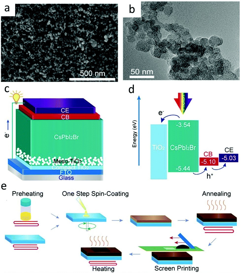
Recently, Gong et al. have introduced an intermediate layer of carbon black between the perovskite film and the carbon rear electrode.48 The device was fabricated with the structure of the perovskite/carbon black/carbon electrode, where carbon black was employed to facilitate the hole extraction. They adopted a one-step spin-coating method with a preheating process for a high-quality perovskite film.58–62 The configuration and band alignment of the device are illustrated in Fig. 4(c) and (d).48Fig. 4(e) depicts the manufacture procedures of the perovskite layer, carbon black interlayer and carbon rear electrode. Obviously, the carbon black interlayer played a role of transition layer between perovskite and carbon rear the electrode, which accelerated hole extraction. It improved the extraction efficiency of holes because of the larger contact area and proper energy band arrangement in the interface perovskite/carbon electrode. As a result, the device achieved a recorded PCE of 13.13%.48 Chu et al. designed a new type of carbon rear electrode with nanoscale carbon black and carbon fiber to improve the perovskite/carbon interface.63 HTL-free PSCs were obtained by using double-layer carbon electrodes (coherent layer and conductive layer), thereby increasing the PCE to 14.1%.63
Moreover, Wei et al. made a thermoplastic carbon film for the black electrode of flexible HTL-free PSCs by mixing carbon black and graphite at low temperatures (<100 °C).52 Under the conditions of carbon film composition (the ratio of graphite to carbon black was 3:1) and hot-press pressure (0.25 MPa), the interface contact between the perovskite and carbon film was optimal.
2.2 Graphene
Among the carbon materials, graphene (a sheet with two-dimensional carbon atoms filled into the honeycomb lattice) has a variety of extraordinary properties. For instance, high charge mobility (1020 cm2 V−1 s−1), good electrical conductivity, outstanding mechanical flexibility and transmittance,67–71 not least the good flexibility and light transmittance of graphene made it suitable for flexible PSCs as a transparent electrode. However, the device structure was either mesoporous or planar, and it was necessary to use high temperature to treat TiO2 and form dense films. The process not only consumed times and energies, but also hindered the manufacture of flexible devices. In the inverted (p–i–n) structure, ETL and HTL collected photo-generated electrons and holes and reached the anode and carbon electrodes, respectively.72 The carbon electrode here was required to be highly transparent within a certain spectral range (visible and infrared). Therefore, graphene is an ideal choice. The SEM image of graphene is shown in Fig. 5(b). The SEM images of bulk graphite (BG) and ultra-thin graphite (UG) are shown in Fig. 5(c)–(f).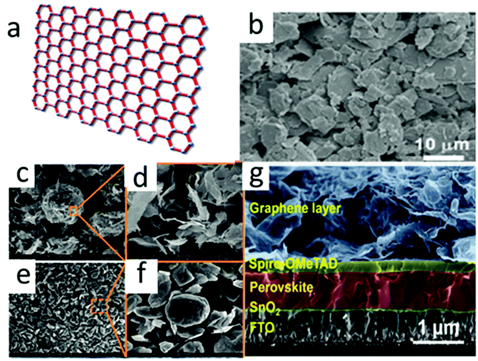 | ||
| Fig. 5 (a) Schematic of graphene. (b) SEM image of graphene.64 Copyright 2015, Royal Society of Chemistry. SEM images at low and high magnifications of (c) and (d) UG and (e) and (f) bulk graphite (BG).65 Copyright 2017, Elsevier. (g) Cross-sectional SEM image of G-PSC.66 Copyright 2019, Royal Society of Chemistry. | ||
In 2015, You et al. applied graphene as a transparent rear electrode in the inverted PSCs for the first time.73 The front electrode (FTO side) and the rear electrode (graphene side) were irradiated under 1 sun illumination, and the PCE were 12.02% and 11.6%, respectively. Graphene was widely used in inverted PSCs and replaced transparent conductive oxide (TCO) as the front electrode.74 By using graphene transparent anodes and organic hole transport materials poly(3,4-ethylenedioxythiophene):poly(styrenesulfonate) (PEDOT:PSS), high-efficiency TCO-free PSCs were prepared. By adding MoO3 and optimizing the thickness of the MoO3 layer between the graphene anode and PEDOT:PSS, the highest PCE of 17.1% was obtained. Simultaneously, the PCE of the device with ITO transparent electrode was 18.8%.74
These studies found that PCE vitally depended on the number of graphene layers.74–76 The performance of the two-layer graphene device was the best and achieved the PCE with 12.37% certified value, while the PCE of the single-layer assembled device was 9.18%.77 Nevertheless, the increased graphene layers resulted in deterioration of PCE (PCE for three and four layers were 11.45% and 11.27%, respectively).77 A large quantity of layers reduced the transmittance of electrodes, and resulted in a decrease in quantities of photons reaching the absorber layer. In 2019, by Zhang et al. showed that graphene-based PSCs (G-PSCs) exhibit a PCE of 18.65%.66 The optimized unpackaged device kept 90% of its initial PCE after aging for 1000 hours at a high temperature of 85 °C. Fig. 5(g) shows the SEM image of the G-PSC structure.
2.3 Carbon nanotubes
Carbon nanotubes had become a promising next-generation black electrode.80 Carbon nanotubes were 1D cylinders coiled with graphene, which had excellent optoelectronic properties similar to graphene. It included single-walled (SWCNT) and multi-walled carbon nanotubes (MWCNTs). The diameter of SWCNTs was generally 1.5 nm.64 The SEM image of the carbon nanotube is shown in Fig. 6(a). As the wall of the tube could be bent, the charge transfers faster as it passes. The band gap of CNTs could also change with the change in diameter, and had a Wf value of −4.95 eV.81–87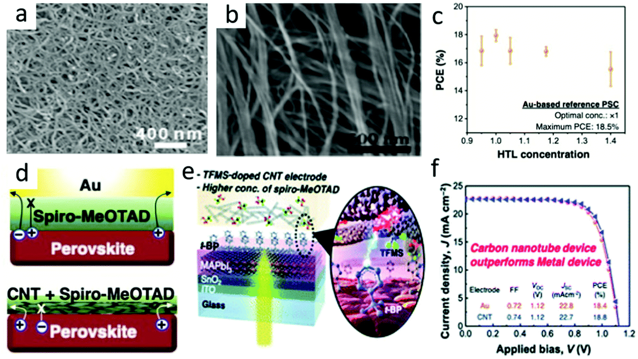 | ||
| Fig. 6 (a) SEM image of CNTs.64 Copyright 2015, Royal Society of Chemistry. (b) Typical SEM image of the CSCNT film.78 Copyright 2018, Wiley. (c) M-PSCs with different Spiro-MeOTAD concentrations. (d) Depiction of the charge flow in M-PSCs (above) and CNT-based PSCs (below). (e) Schematic of the optimized TFMS-doped CNT electrode PSC device. (f) J–V curves of the Au-based PSCs (orange circle) and the optimized TFMS-doped CNT-PSCs (blue triangle).79 Copyright 2020, Royal Society of Chemistry. | ||
Furthermore, the mechanical property of CNTs was proved to be extremely beneficial for the exploitation of flexible PSCs.88,89 Compared with the high treatment temperature of the carbon black/graphite composite electrode (above 450 °C), CNT films could be integrated into PSCs without any sintering, since remarkable optical characteristic and flexibility CNTs were very prospective in flexible PSC electrode materials. Luo et al. reported a cross-stacked carbon nanotube (CSCNT) film,78 and later used an SnO2-coated carbon nanotube (SnO2@CSCNT) film as the electrode in flexible inverted PSCs in their work.89 Compared with devices without SnO2 coating, flexible inverted PSCs with SnO2@CSCNT cathodes had significantly improved photovoltaic performance. The results indicated that SnO2@CSCNT was a promising cathode material for long-term PSC operation. The typical SEM image of the CSCNT film is shown in Fig. 6(b).
Jeon et al. developed a vapor doping method based on ex situ triflic acid (TFMS), which minimized the interaction with t-BP and shown the maximum doping effect.79 In the case of traditional M-PSCs, an increase in the concentration of 2,2,7,7-tetrakis(N,N-di-p-methoxyphenylamine)-9,90-spirobifluorene (Spiro-MeOTAD) in HTL would decrease the PCE (Fig. 6(c)). It was in that the increase in HTL concentration resulted in a thicker Spiro-MeOTAD layer, causing a decrease in the hole transport capacity and vice versa.79 However, it did not happen in the case of CNT lamination PSCs, as CNTs had already extracted holes in the interface before Spiro-MeOTAD restricted hole extraction (Fig. 6(d)). Combined the optimized carbon nanotubes and Spiro-MeOTAD (Fig. 6(e)), the best PCE of C-PSCs was higher than that of M-PSCs and reached 18.8% (Fig. 6(f)).79 This was due to the superior hole selectivity of carbon nanotubes and the improvement of electrical conductivity by doping TFMS.
In conclusion, from a view of the application, the performance of graphene as a transparent electrode is the best due to good conductivity, high flexibility and light transmittance.74 Carbon nanotubes are suitable to be counter electrodes because of their unique structure to promote hole extraction,90 while carbon black can increase the pores of carbon paste, promote charge transfer and improve interface contact.48 Therefore, it is reasonable to believe that if the carbon materials will be utilized as the basic electrode material, the PCE will possibly catch up with that of conventional M-PSCs.
3. Three types of C-PSC progress
According to the difference between the device structure and the carbon electrode deposition process, C-PSCs were divided into three types, namely, meso, embedment, and paintable C-PSCs, which are shown in Fig. 7, 8 and 9, respectively. The comparison with the parameters of M-PSCs is shown in Table 2. From these results, it can be seen that the PCE of C-PSCs was still lower than that of M-PSCs, but the efficiency had been steadily improved. Thus far, the performance of paintable C-PSCs was the best.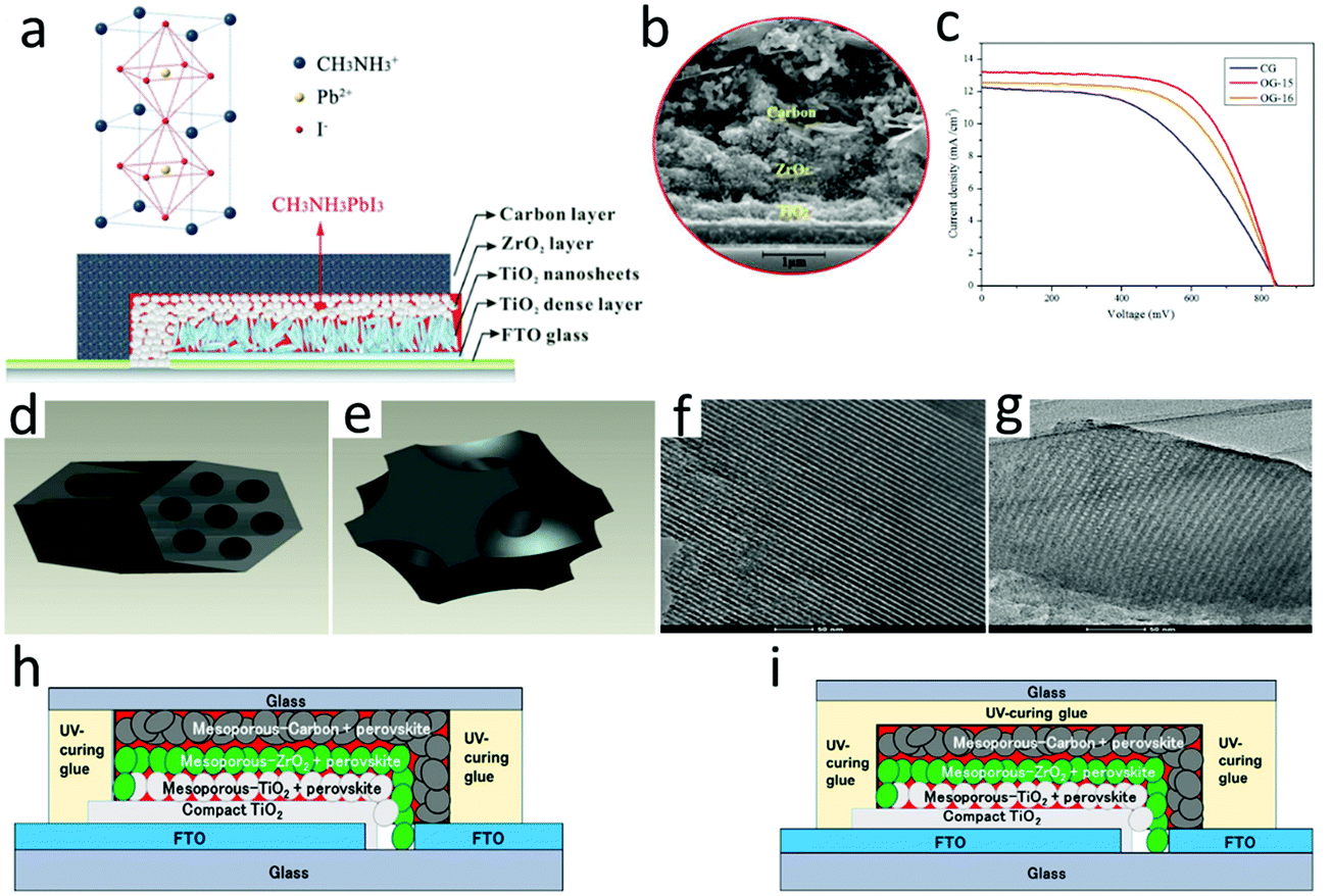 | ||
| Fig. 7 (a) Schematic of a hole-conductor-free mesoscopic TiO2/CH3NH3PbI3 heterojunction solar cell based on anatase nanosheets and carbon counter electrodes.111 Copyright 2014, American Chemical Society. (b) SEM image of the devices.112 Copyright 2015, Royal Society of Chemistry. (c) Photocurrent density–voltage curves of mesoscopic solar cells with carbon black/graphite electrode (CG), C-FDU-15/graphite electrode (OG-15) and C-FDU-16/graphite electrode (OG-16) counter electrodes. (d) Assembled carbon framework structure of C-FDU-15. (e) Assembled carbon framework structure of C-FDU-16. (f) TEM image of C-FDU-15 viewed in the (110) direction. (g) TEM image of C-FDU-16 viewed in the (110) direction.113 Copyright 2014, Royal Society of Chemistry. Diagram of the fabricated three-layer PVK device: (h) side-sealed and (i) over-sealed cells.114 Copyright 2016, Wiley. | ||
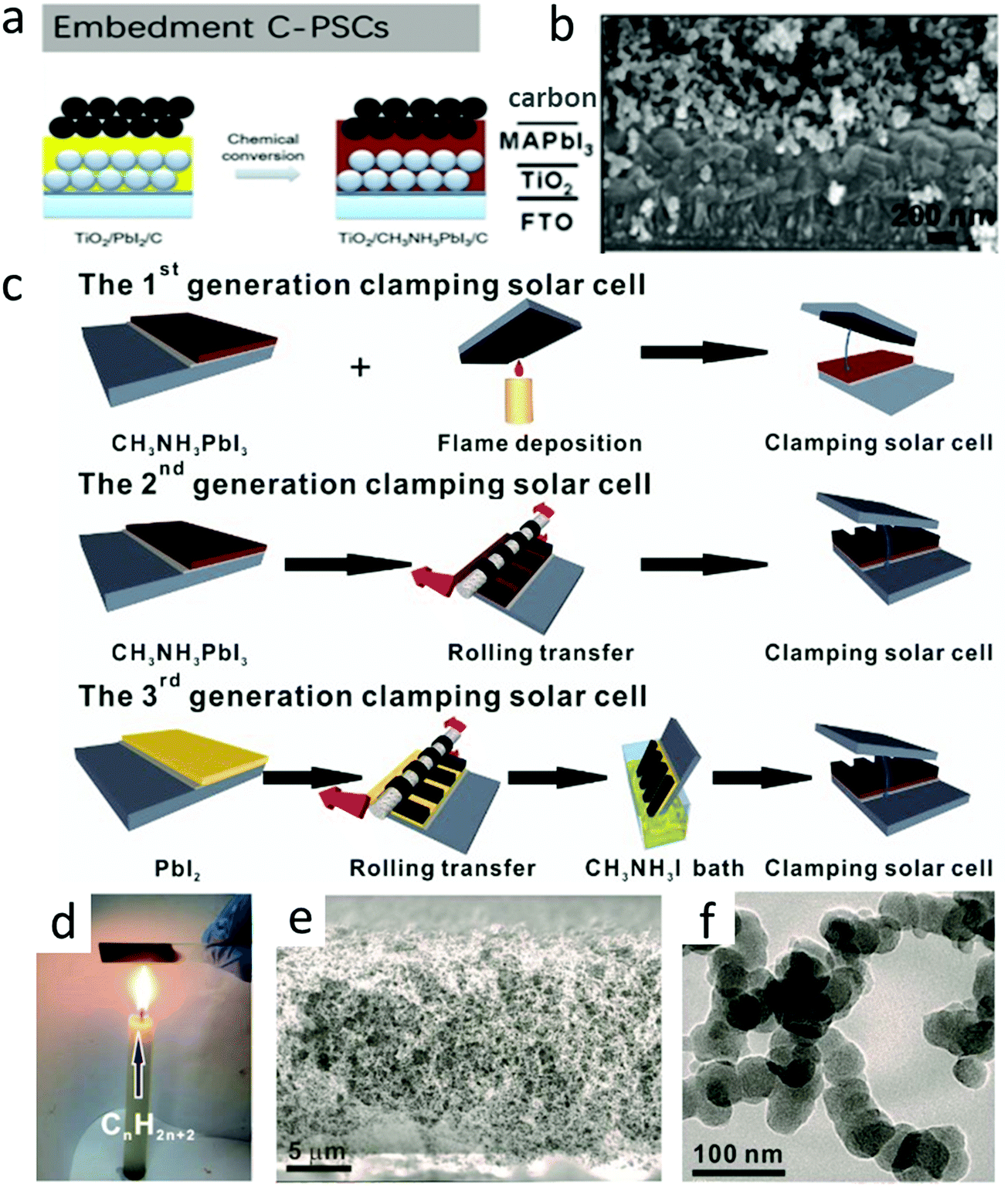 | ||
| Fig. 8 (a) Embedment C-PSCs developed by Wei et al.56 Copyright 2014, Royal Society of Chemistry. (b) Cross-sectional SEM images of embedment C-PSCs.103 Copyright 2014, Wiley. (c) (top) Fabrication process of the first-generation clamping solar cells by simply clamping an FTO-supported candle soot film and a CH3NH3PbI3 photoanode. (Middle) Fabrication of the second-generation clamping solar cells by rolling transfer-assisted clamping. (bottom) Fabrication of the third-generation clamping solar cells by chemically promoted rolling transfer clamping, with a CH3NH3I bath for the in situ conversion of PbI2 to CH3NH3PbI3 partially embedding the soot electrode. (d) A digital photo portraying the flame deposition of the candle soot. (e) Cross-sectional SEM image of the sponge-like candle soot film. (f) TEM image of the as-prepared bi-continuous network of chain-like candle soot nanoparticles.56 Copyright 2014, Royal Society of Chemistry. | ||
 | ||
| Fig. 9 (a) Fabrication process of paintable carbon-based PSCs. (b) Cross-sectional SEM image of the solar cell device architecture.106 Copyright 2016, Wiley. (c) Microscopic curing mechanism during the formation of C1 and C2 films. (d) Cross-sectional SEM images of PSCs with the C1 film and C2 film as electrodes.28 Copyright 2018, Wiley. | ||
| V OC (mV) | J SC (mA cm−2) | FF (%) | PCE (%) | Ref. [years] | |
|---|---|---|---|---|---|
| M-PSCs | 993 | 20.00 | 73.00 | 15.00 | 20133 |
| 1130 | 22.75 | 75.01 | 19.30 | 201491 | |
| 1060 | 24.70 | 77.50 | 20.20 | 201592 | |
| 1180 | 22.80 | 81.00 | 21.80 | 201693 | |
| 1110 | 25.00 | 81.70 | 22.60 | 201794 | |
| 1114 | 24.91 | 81.29 | 23.20 | 201895 | |
| 1160 | 24.90 | 81.40 | 23.56 | 201996 | |
| 1181 | 25.14 | 84.80 | 25.20 | 202097 | |
| Meso C-PSCs | 878 | 12.40 | 61.00 | 6.64 | 201325 |
| 858 | 22.80 | 66.00 | 12.84 | 201498 | |
| 867 | 22.93 | 67.00 | 13.41 | 201599 | |
| 921 | 19.21 | 78.00 | 13.89 | 2016100 | |
| 1050 | 20.20 | 75.00 | 15.90 | 2017101 | |
| 1080 | 23.33 | 76.20 | 19.20 | 201828 | |
| 910 | 19.64 | 66.00 | 12.07 | 2021102 | |
| Embedment C-PSCs | 950 | 17.20 | 71.00 | 11.60 | 2014103 |
| 880 | 18.00 | 80.00 | 12.67 | 201564 | |
| 920 | 21.50 | 77.00 | 15.23 | 2017104 | |
| 1070 | 23.44 | 61.00 | 15.38 | 201830 | |
| 930 | 23.47 | 75.00 | 16.37 | 2019105 | |
| 1050 | 20.93 | 68.97 | 15.18 | 202072 | |
| Paintable C-PSCs | 900 | 16.78 | 55.00 | 8.31 | 201426 |
| 1002 | 21.30 | 63.40 | 13.53 | 201564 | |
| 1040 | 21.27 | 65.00 | 14.38 | 2016106 | |
| 1070 | 21.44 | 68.00 | 15.66 | 2018107 | |
| Paintable C-PSCs | 910 | 21.04 | 72.00 | 14.55 | 2019108 |
| 1095 | 23.90 | 68.00 | 17.71 | 2020109 | |
| 1040 | 21.50 | 70.44 | 15.81 | 2021110 | |
3.1 Meso C-PSCs
For HTL-free meso PSCs, the perovskite layer could not only be used as a light absorbing layer, but also played the role of hole transport, which made the use of hole transport materials redundant and simplified the preparation process of the device.115–120 The meso C-PSCs exploited by Ku et al. was the most representative,25 which had a schematic of a typical HTL-free meso C-PSCs, as shown in Fig. 7(a). It included three mesoporous layers (i.e. TiO2, ZrO2, carbon), which were used as ETL, insulating layer and HTL, respectively. The preparation process of the device included that etched FTO and then deposited a dense TiO2 layer, mesoporous TiO2 layer, mesoporous ZrO2 electron blocking layer, and mesoporous carbon electrode by screen printing. The SEM image confirmed that the thickness of the device was only 5–10 μm in Fig. 7(b), wherein TiO2 and ZrO2 mesoporous layers were made of nanoparticles, while carbon mesoporous layers (at least a few microns thick) were composed of carbon black and graphite in a certain proportion. After assembling the device with screen printing technology, the device was annealed at high temperatures to improve its mechanical strength. Finally, the perovskite precursor solution was dropped onto the device surface, and the solution was infiltrated into the multi-layer mesoporous structure to obtain meso C-PSCs. Since the thickness of the entire device was at least a few microns, complete penetration of the solution into the mesoporous structure was a significant issue for meso C-PSCs.In the initial study of meso C-PSCs, the solution of PbI2 and MAI was employed to the device via a one-step deposition technique, which achieved a PCE with 6.6%.25 The inferior performance was due to the poor infiltration of the perovskite precursor solution in the device. To improve solution infiltration, Xu et al. applied an ordered porous carbon material as the carbon electrode, which boosted the solution infiltration and lightly increased the PCE to 7%.113 As illustrated in Fig. 7(c), the photocurrent density–voltage characteristic (J–V) curve of meso C-PSCs was plotted using OG-15, OG-16 and CG as counter electrodes, respectively.113Fig. 7(d) and (e) represent the assembled framework C-FDU-15 and C-FDU-16, respectively.113Fig. 7(f) shows the TEM image of C-FDU-15 seen in the (110) direction, and Fig. 7(g) shows the TEM image of C-FDU-16 viewed from the same direction.113 A two-step technique was also explored for meso C-PSCs by Han's group,111 which involved pre-deposition of PbI2, and then reached reaction in MAI solution to generate MAPbI3. By employing the TiO2 nanosheet as the ETL, the meso C-PSCs exhibited the best PCE of 10.6%,111 which enhanced to 11.6% after altering the graphite size and thickness of the carbon counter electrode.112 Baranwal et al. evaluated the stability of the PCE of meso C-PSCs.114 The results indicated that the efficiency of the encapsulated meso C-PSCs was not almost degraded at 100 °C, which indicated that the high thermal stability of the device had a chance to be achieved. Although the thick carbon layer could play a role in reducing the perovskite layer from being affected by moisture degradation, it must also avoid direct exposure of the rear electrode. There were two kinds of sealing positions of the device, as illustrated in Fig. 7(h) and (i). These results indicated that meso C-PSCs had the opportunity to achieve high-efficiency PSCs.114
3.2 Embedment C-PSCs
As an improved version of meso C-PSCs, embedment C-PSCs not only simplified the fabrication process, but also prevented the perovskite layer from being destroyed at high temperatures.121–124 Embedment C-PSCs was first developed by Wei et al. (Fig. 8(a)).56 By spin-coating a carbon paste on the PbI2 layer, which was followed by converting PbI2 into lead halide perovskite (LHP). In another method, a seamless interface between the perovskite layer and the carbon layer was formed by screen printing carbon/MAI ink on PbI2 to form LHP in situ. Therefore, compared with the use of carbon ink, the charge recombination was reduced.19,56 The SEM image of the device prepared with the C + CH3NH3I ink mixture (Fig. 8(b)) presented a layer-by-layer structure.103 As shown in Fig. 8(c), Wei et al. systematically focused on the optimization of the perovskite/carbon interface by progressively evolving three generations of clamped solar cells.56 The reliable contact of the first generation, between the perovskite and the candle soot could not be guaranteed due to the insufficient conductivity of the candle soot and uncontrollable clamping method, resulting in high internal resistance and poor photovoltaic performance. In order to solve these issues, the second generation of splint solar cells exhibited improved graphitization and electrical conductivity by the annealing of the candle soot and the interface contact. However, the filling factor (FF) and PCE remained mismatching for Spiro-MeOTAD-based devices, which might be related to the inferior interface contact between the perovskite and candle soot. Finally, the problem was basically solved in the third generation of clamped devices. The improved clamping technique resulted in a significant improvement in PCE (11.02%) and performance reproducibility. Fig. 8(d) illustrates the classical method of obtaining candle soot, which was very convenient for the large-scale preparation of carbon nanoparticles. A piece of glass was put upon the candle flame, and a micron-thick candle soot film could be obtained in seconds. According to the SEM image in Fig. 8(e), it could be found that it was a loose sponge-like structure. The TEM image in Fig. 8(f) further revealed that the candle soot had a nano-chain structure, which was roughly composed of 30 nm nano-particle strings.Carbon black was often used in the work of embedment of C-PSCs. However, the poor connectivity of carbon black would lead to an inferior interfacial contact. The addition of other adhesives would increase the connectivity, but prevent the infiltration of the solution and inhibit the conversion of PbI2 into MAPbI3. In order to solve this issue, the bonding properties of other carbon materials (carbon black, graphite and MWCNTs) were compared. Finally, it was concluded that the FF values of the three carbon materials were very different, in the order of graphite (0.64) < carbon black (0.65) < MWCNTs (0.75).64
In 2019, Yang et al. reported embedment C-PSCs based on carbon nanotubes. Carbon nanotubes were coated on PbI2 and then immersed in CH3NH3I solution for 12 h to form a CH3NH3PbI3 perovskite layer. Finally, the prepared CH3NH3PbI3 perovskite layer was annealed on a hot plate at 100 °C for 10 min to obtain a complete device. On the basis of this device, they added a ferroelectric oxide (PbTiO3) between the ETL and the perovskite layer. The PbTiO3 was formed on TiO2 by coating TiO2 with (Pb(OAc)2·3H2O), and then annealing at 450 °C for 1 h. The PbTiO3 could provide a larger internal electric field and inhibit the non-radiative recombination of carriers, and the corresponding PCE of device reached 16.37%.
3.3 Paintable C-PSCs
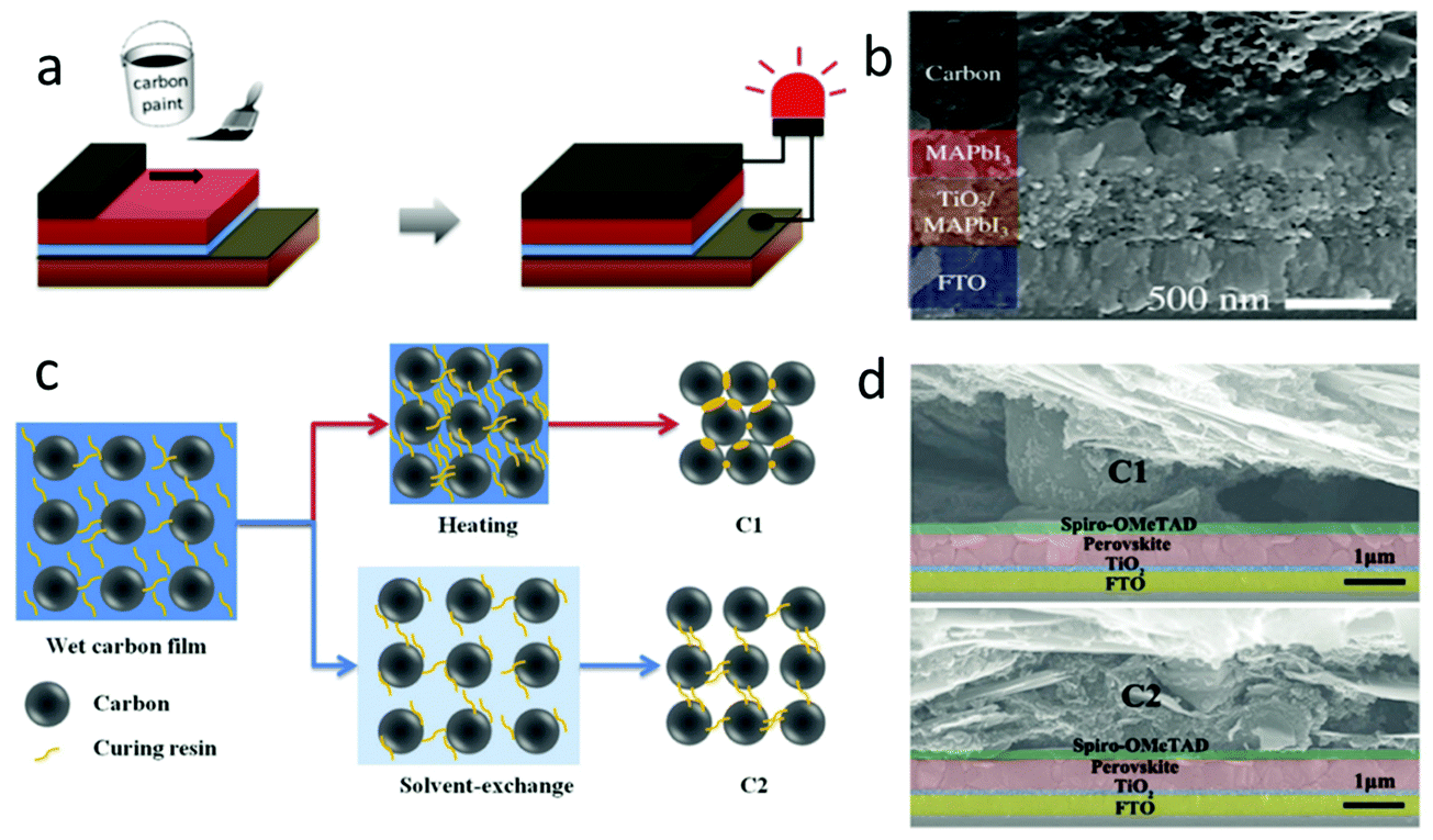
It was well known that the inferior contact between perovskite layer and carbon electrode was the main reason for the low PCE. In order to improve this issue, a kind of carbon paste coating was developed. This carbon paste was mainly composed of carbon materials, additives, polymers and non-polar solvents. Therefore, the previous clamping C-PSCs had been improved to paintable C-PSCs.125,126 In this kind of C-PSCs, the morphology influence of perovskite films on the interface was very important, which would affect the performance of the device.28 According to the process shown in Fig. 9(a), the carbon paste was printed on the perovskite layer, and then the paintable C-PSCs could be obtained by annealing 30 min at low temperatures (100 °C).106 The interfacial contact between the perovskite layer and the carbon electrode was improved by using an isopropanol/cyclohexane solvent, as shown in Fig. 9(b).106 The carbon paste was printed on the pre-deposited LHP layer by painting or doctor blading, so the structure of the device had only four layers (carbon, LHP, TiO2, FTO).127Zhang et al. applied a commercial carbon paste to paintable C-PSCs for the first time.26 By systematically altering the thickness of the TiO2 layer, the device obtained a PCE of 8.3%. In the beginning, the PCE of paintable C-PSCs was very low, but the simplest manufacturing process continued to inspire researchers to enhance the efficiency of the device. By optimizing the ratio of paint composition (carbon black and graphite), Yang et al. obtained a PCE of 10.2%.128 In 2015, Wei et al. developed a flexible carbon paste printing on the LHP layer, which effectively avoided the negative influence of the solvent on the perovskite film, and finally obtained a PCE with 13.5%.52
The research on the stability of paintable C-PSCs had been reported by literatures.129,130 Wei et al. compared the effects of epoxy resin and Ag coating on the carbon electrode.131 Epoxy resin was a kind of polymer in carbon paste and had superior water resistance. Compared with the pure carbon electrode, carbon paste as the electrode had a better hydrophobicity. The Ag coating could enhance the hydrophobicity. In addition, the Ag coating could also improve the conductivity of the carbon electrode. Because perovskite was easily degraded by moisture, hydrophobicity was very important.131 This was proved by the environmental stability measurement. The device with epoxy resin had higher stability, and the Ag coating acted like the icing on the cake.131
Zhang et al. exploited a self-adhesive macroporous carbon film by solvent exchange at room temperature.28 In the previous process, the solvent in the carbon paste was removed by high-temperature volatilization, which seriously affected the flexibility and porosity of the carbon paste, labeled as C1. It was found that ethanol could effectively inhibit the curing of carbon paste during solvent exchange. Fig. 9(c) depicts the microscopic curing mechanism of carbon paste.28 After the exchange process was completed, the carbon film fell off from the glass substrate and formed a self-supporting film, which was marked C2. This method can avoid high-temperature curing. Fig. 9(d) shows the SEM images of devices with C1 and C2 as black electrodes, respectively.28 It was found that there was a large gap between C1 and the Spiro-MeOTAD layer, while there was almost no gap between C2 and the Spiro-MeOTAD layer, and hence, it had a better interfacial contact.
There were obvious differences among the three kinds of C-PSCs in the preparation process, especially in the preparation and deposition of carbon paste. The multi-layer mesoporous structure in meso C-PSCs limited the complete conversion of pre-deposited PbI2.99–101,132 In the preparation of embedment C-PSCs, the TiO2 layer and the carbon layer should be deposited separately by a two-step method when pre-depositing PbI2.71,133–135 For paintable C-PSCs, it was deposited layer by layer. No matter it was the one-step method, the two-step method or other development methods, it could be applied. Due to its superior stability, low cost of production and large market potential, C-PSCs had become a critical part of the PSC field.136–141Table 3 lists the fabrication parameters of different techniques. It can be seen that the PCE of paintable C-PSCs exhibited the best.
| Paste composition | Fabrication technique | Thermal treatment | Sheet resistance (Ω cm2) | Thickness (μm) | PCE (%) | Ref. [year, journal] |
|---|---|---|---|---|---|---|
| Carbon black (CB), bulk graphite (BG), ultrathin graphite (UG), polymethyl methacrylate (PMMA). | ||||||
| CB/flaky graphite | Meso | 400 °C for 30 min | 10.49 | 10 | 4.08 | 2013, Sci. Rep.25 |
| CB/spheroidal graphite | Meso | 400 °C for 30 min | 8.02 | 10 | 6.64 | 2013, Sci. Rep.25 |
| 2 g CB (particle size 30 nm), 6 g graphite powder, 1 g ZrO2 (particle size 20 nm), 1 g hydroxypropyl cellulose in 30 mL terpineol | Meso | 400 °C for 30 min | 11.47 | 9 | 11.63 | 2015, J. Mater. Chem. A112 |
| 9 g graphite powder (particle dimension <20 mm), 3 g CB, 1 g ZrO2 (particle dimension <100 nm), 15 g ethylcellulose in 18 g terpineol | Embedment | 400 °C for 30 min | 56 | 25 | 10.7 | 2018, Electrochim. Acta142 |
| 5 g graphite, 1 g CB (particle size 30 nm), 1 g ZrO2 (particle size 20 nm), terpineol (30 mL) | Embedment | 400 °C for 30 min | Not reported | Not reported | 13.7 | 2015, Nano Lett.143 |
| BG, CB, hydroxypropyl cellulose, terpineol | Embedment | 400 °C for 30 min | 5–20 | 5–16 | 12.63 | 2017, Carbon65 |
| UG (obtained by exfoliation of BG), CB, hydroxypropyl cellulose, terpineol | Embedment | 400 °C for 30 min | 5–25 | 5–16 | 14.01 | 2017, Carbon65 |
| Carbon material (graphite:CB = 3:7), hydroxypropyl cellulose, terpineol |
Embedment | 400 °C for 30 min | 23 | 11 | 15.7 | 2018, Nano Energy144 |
| 4 g graphite, 1 g CB, 0.6 g ZrO2, in ethanol | Embedment | 400 °C for 30 min | 30.5 | Not reported | 3.36 | 2018, Solid State Commun.145 |
| 3.8 g graphite, 0.95 g CB, 0.57 g ZrO2, 0.28 g polystyrene spheres in ethanol | Embedment | 400 °C for 30 min | 56.70 | Not reported | 3.87 | 2018, Solid State Commun.145 |
| 3.6 g graphite, 0.9 g CB, 0.54 g ZrO2, 0.56 g polystyrene spheres in ethanol | Embedment | 400 °C for 30 min | 68.30 | Not reported | 4.10 | 2018, Solid State Commun.145 |
| 2.8 g graphite, 0.7 g CB, 0.42 g ZrO2, 1.68 g polystyrene spheres in ethanol | Embedment | 400 °C for 30 min | 180.70 | Not reported | 3.13 | 2018, Solid State Commun.145 |
| 6.5 g graphite, 2 g CB, 1 g ZrO2, 1 g hydroxypropyl cellulose, 30 mL terpineol | Embedment | 400 °C for 30 min | 35.00 | 11 | 12.4 | 2017, ACS Appl. Mater. Interfaces137 |
| 6.5 g BdG, 2 g CB, 1 g ZrO2, 1 g hydroxypropyl cellulose, 30 mL terpineol | Embedment | 400 °C for 30 min | 16.00 | 9.6 | 13.60 | 2017, ACS Appl. Mater. Interfaces137 |
| CB (5 wt%), Al2O3 (5 wt%), graphite (10 wt%), ethyl cellulose (20 wt%), terpineol (60 wt%) | Embedment | 125 °C for 10 min, 325 °C for 10 min, 375 °C for 10 min, 400 °C for 30 min | Not reported | 4–5 | 12.12 | 2017, ACS Appl. Mater. Interfaces146 |
| 2 g CB (particle size 30 nm), 6.5 g graphite, 1 g ZrO2 (particle size 20 nm), 1 g hydroxypropyl cellulose, 30 mL terpineol | Embedment | 400 °C for 30 min | 8.98 | 10 | 14.15 | 2018, J. Phys. Chem. C147 |
| 15 mg mL−1 CB in 2-propanol | Embedment | 100 °C for 60 min | Not reported | Not reported | 7.55 | 2014, Angew. Chem., Int. Ed.103 |
| 15 mg mL−1 CB, 10 mg mL−1 CH3NH3I in 2-propanol | Embedment | 100 °C for 60 min | Not reported | Not reported | 10.03 | 2014, Angew. Chem., Int. Ed.103 |
| 20 wt% polyvinyl acetate, 80 wt% carbon material (graphite:CB = 1:0) |
Paintable | 85 °C for 15 s | 1.11 | 40 | 10.27 | 2015, Carbon52 |
| 20 wt% polyvinyl acetate, 80 wt% carbon material (graphite:CB = 1:0) |
Paintable | 85 °C for 15 s | 1.11 | 40.00 | 10.27 | 2015, Carbon52 |
| 20 wt% polyvinyl acetate, 80 wt% carbon material (graphite:CB = 5:1) |
Paintable | 85 °C for 15 s | 0.75 | 40.00 | 11.43 | 2015, Carbon52 |
| 20 wt% polyvinyl acetate, 80 wt% carbon material (graphite:CB = 3:1) |
Paintable | 85 °C for 15 s | 0.69 | 40.00 | 13.53 | 2015, Carbon52 |
| 20 wt% polyvinyl acetate, 80 wt% carbon material (graphite:CB = 2:1) |
Paintable | 85 °C for 15 s | 0.61 | 40.00 | 12.47 | 2015, Carbon52 |
| Commercial carbon paste (CC, Shenzhen DongDaLai Chemical Co., Ltd) | Paintable | 100 °C for 30 min | 6.40 | 10.00 | 16.10 | 2016, Nano Energy148 |
| Graphite flakes (10 mm):CB (40 nm) = 3:1 in ethyl acetate |
Paintable | Not reported | 17.00 | 65.00 | 4.47 | 2016, Nanoscale27 |
| Graphite flakes (10 mm):CB (40 nm): nano-graphite powder (400 nm) = 1:1:2 in ethyl acetate |
Paintable | Not reported | 70.00 | 65.00 | 5.31 | 2016, Nanoscale27 |
| Graphite flakes (10 mm):CB (40 nm):nano-graphite powder (400 nm) = 1:1:2 in ethyl acetate |
Paintable | Not reported | 100.00 | 65.00 | 6.16 | 2016, Nanoscale27 |
| Graphite, CB, PMMA (binder), Y-037 (solvent) | Paintable | 100 °C for 20 min | Not reported | 10.00 | 10.22 | 2018, Appl. Surf. Sci.149 |
| Commencial carbon paste (Guangzhou Saidi Technology Co., Ltd). | Paintable | 100 °C | 58.60 | 31.90 | 19.20 | 2018, Adv. Funct. Mater.28 |
| Commencial carbon paste (Guangzhou Saidi Technology Co., Ltd) | Paintable | 100 °C (until the residual solvent is totally evaporated) | 10.90 | 34.50 | 15.20 | 2018, Adv. Funct. Mater.28 |
| The layer was soaked in ethanol to remove the residual solvent Commercial carbon paste (Shenzhen DongDaLai Chemical Co., Ltd) | Paintable | Not reported | Not reported | Not reported | 17.78 | 2019, Appl. Surf. Sci.150 |
| Commercial carbon ink (Jujo printing supplies & technology (pinghu) Co., Ltd) | Meso | 100 °C for 15 min | Not reported | 11.20 | 11.92 | 2018, Org. Electron.151 |
Although C-PSC-related research had achieved excellent results, the inferior interface contact between the perovskite film and the carbon electrode remained to be solved.
4. Interface engineering of C-PSCs
Owing to poor adhesion of carbon materials and inferior contact with the perovskite layer interface, a large amount of charge recombination occurred in the work of HTL-free C-PSCs. The interface contact between the perovskite layer and the carbon electrode was considered to be the main reason for the poor performance of photovoltaic devices.28 Hence, it was the main task to study the interface engineering between the perovskite layer and the carbon layer.1524.1 Energy alignment
For C-PSCs, appropriately changing the energy band arrangement can increase the hole extraction efficiency, and the PCE will also increase. Tian et al. tuned the Wf value by changing the oxygen content in the carbon electrode to improve the interface contact and reduce charge recombination.144 The Subodh G. Mhaisalkar group found in C-PSCs that screen printing a p-type inorganic spinel Co3O4 film on the interface between perovskite and carbon electrodes could also enhance energy level matching, PCE and stability.153It was found that increasing the oxygen content in the carbon electrode not only elevated the Wf value but also optimized the interface contact with perovskite. It was obvious that the development of meso C-PSCs was hindered by the poor interface. As illustrated in Fig. 10(a), Tian et al. proposed that the oxygen content in the carbon electrode would change its Wf and the interface contact with the perovskite layer. This was because oxygen ions could make the carbon electrode interact with perovskite chemically through lead–oxygen coordination, making the interface contact more close.154,155 Simultaneously, the appropriate increase of oxygen content also boosted the graphitic interplanar distance, increased the specific surface area of carbon materials,156,157 and further improved the interface contact between a carbon electrode and perovskite.65 Accordingly, Tian et al. deduced that the high oxygen–carbon electrode could collect holes more effectively, and reduce the charge recombination phenomenon. Besides, due to the different hybrid ratio of sp3:sp2, the oxygen content altered the electronic structure of carbon materials to become hole transport materials similar to graphene oxide, which further increased the selectivity of hole extraction.158,159 Thus, the oxygen management of carbon electrodes had the opportunity to improve the performance of meso C-PSCs. The Wf value of ODC and ORC were 5.0 eV and 5.2 eV, respectively. The Wf value of the ORC-based carbon electrode was in good agreement with the maximum valence band of perovskite, which improved the hole extraction of the device. Fig. 10(b) shows a cross-sectional SEM image of a perovskite layer formed in a carbon electrode based on ODC and ORC.144
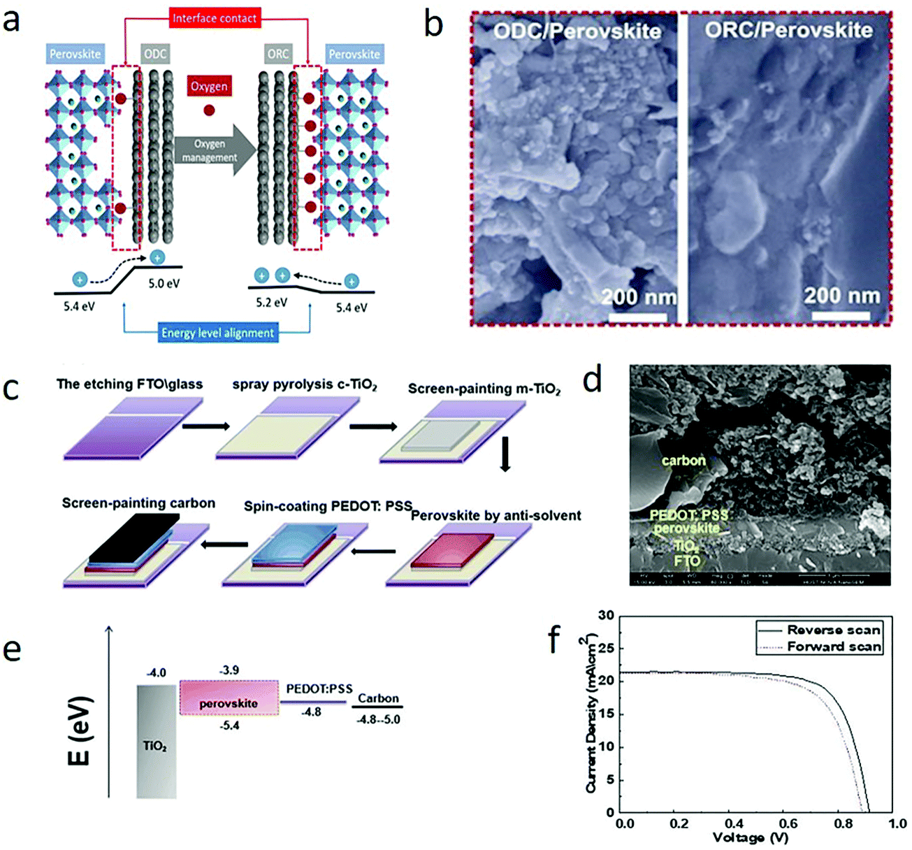 | ||
| Fig. 10 (a) Schematic of oxygen-deficient carbon black (ODC) and oxygen-rich carbon black (ORC), interfacial contact and energy level alignment of the materials. (b) Cross-sectional SEM images of the perovskite formed in ODC- and ORC-based CEs.144 Copyright 2018, Elsevier. (c) Schematic of the fabrication process of C-PSCs: FTO/compact TiO2/mesoscopic TiO2/perovskite/PEDOT:PSS/C layer. (d) Cross-sectional SEM image of the C-PSC device. (e) Energy band diagram of C-PSCs. (f) J–V characteristics at RS and FS of a representative C-PSC under simulated AM 1.5G illumination (100 mW cm−2) condition.108 Copyright 2019, Royal Society of Chemistry. | ||
In 2019, Wang et al. employed a kind of high conductivity and low-temperature carbon paint to paintable C-PSCs.108 The carbon paint had good perovskite compatibility and conductivity, and the final PCE was 11.7%.108 The interfacial contact was improved and hole extraction was increased by introducing hole transport layer (3,4-ethylenedioxythiophene:polystyrene sulfonate (PEDOT:PSS)). Fig. 10(c) shows the fabrication process of this device. The cross-sectional scanning electron microscopic image of cryogenic C-PSCs is shown in Fig. 10(d). It was worth noting that it was difficult to match PEDOT:PSS (Wf ∼ 4.8 eV) and carbon (Wf ∼ 4.8–5.0 eV), as shown in Fig. 10(e). Therefore, the close contact between perovskite and carbon electrode accelerated the hole collection and achieved 14.55% PCE.108
4.2 Hysteresis effect
In C-PSCs, the hysteresis depended on the voltage scanning rate. As the voltage scanning rate increased, the hysteresis became pronounced. The obtained rate and voltage, as well as the direction of the bias voltage, would affect the shape of the J–V curve and the photovoltaic parameters of the device. Through the comparison of the data, the J–V curve measured from the reverse bias voltage had better performance than the J–V curve measured from the forward bias voltage.133,160–163 The PSCs showed dramatic instability under atmospheric conditions.127,164–166 To overcome this detrimental effect, it was important to find out the cause of this phenomenon in C-PSCs. Many scholars believe that the migration of methylammonium (CH3·NH3+), iodide (I−), and photogenerated ions as well as the extreme effect of J–V measurement would process on the alignment of the J–V curve, thus reducing the stability of the device.167–172 Here, we are discussing the hysteresis effect of C-PSCs.The HTL-free C-PSCs not only reduced the cost but also increased the stability. However, the performance of the TiO2-based ETL was unstable due to the hysteresis phenomenon.173,174 Therefore, the non-hysteresis phenomenon C60 was chosen as the ETL, to form the All-C-PSCs. Meng et al. fabricated a FTO/C60/MAPbI3/carbon device structure, in which a PCE of C60-based device was 15.38%, while that of TiO2-based device was only 12.06%.30 The cross-sectional SEM image of the All-C-PSCs is shown in Fig. 11(a). The C60 value effectively improved the electron extraction, suppressed the charge recombination and reduced the sub-band gap state at the interface with the perovskite. Furthermore, the All-C-PSCs prevented moisture from entering the perovskite layer and had superior operation stability in a humid environment. Graphene was further used as a transparent conductive electrode to make it real All-C-PSCs and finally achieved 13.93% PCE. The high performance of the All-C-PSCs came from the bonding flexibility and electronic versatility of carbon materials.175–179 The SEM image of the All-C-PSCs is shown in Fig. 11(b), where the thickness of the carbon layer was about 20 μm, which prevented moisture from infiltration into the perovskite.30Fig. 11(c) shows the J–V curve of the All-C-PSCs based on graphene transparent electrodes. The reverse scan was 0.35% higher than the PCE of the forward scan.30Fig. 11(d) shows the reverse and forward scan J–V curves of C60 and TiO2 ETL, under the condition of AM 1.5G 100 mW cm−2.30 It can be seen that the TiO2-based C-PSCs showed an obvious hysteresis. When replaced by C60, the efficiency of electron extraction was enhanced and the J–V hysteresis was eliminated.30
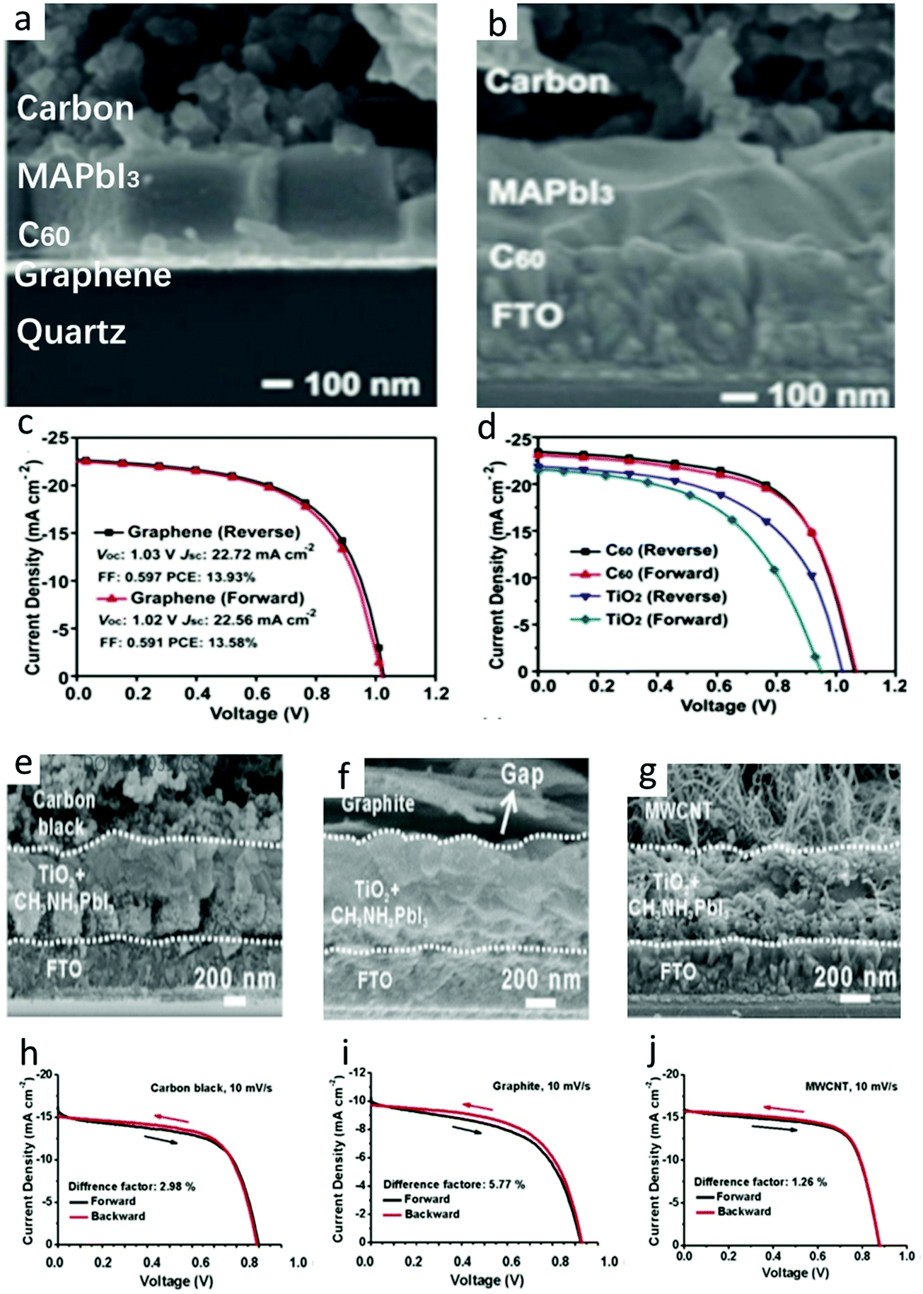 | ||
| Fig. 11 (a) Cross-sectional SEM images of the real all carbon-based PVSCs using the graphene-based transparent conductive electrodes. Cross-section SEM images of the cell architecture at (b) 2000× magnification. (c) J–V curves of the real all C-PSCs using the graphene-based transparent conductive electrodes. (d) J–V curves of the best PSCs with C60 or TiO2 ETLs measured with the forward and reverse scan.30 Copyright 2018, Wiley. Cross-sectional SEM images of embedment C-PSCs with carbon electrodes made of (e) carbon black, (f) graphite, and (g) MWCNTs. Investigation on the hysteresis behavior of the device assembled from (h) carbon black, (i) graphite and (j) MWCNTs (scanning at 10 mV s−1).64 Copyright 2015, Royal Society of Chemistry. | ||
As shown in Fig. 11(h)–(j), there was almost no difference between the forward and reverse directions of the J–V curves of carbon black and MWCNTs at the same scanning rate, indicating that the hysteresis of the two materials was very small. However, there was an obvious difference in the J–V curve of graphite, which mean that there was a large hysteresis phenomenon in graphite. Because the three kinds of carbon materials had similar cell configuration and device structure, it was considered that the effect of hole transfer on the hysteresis effect was different if the contact between carbon electrode and perovskite interface was different.127 Through the study of the hysteresis effect of three kinds of carbon materials, MWCNT was expected to prepare high-efficiency C-PSCs without hysteresis.127
4.3 Passivation defect
The perovskite layer in meso-C-PSCs was formed by infiltrating the mesoporous layer.66,78,182–184 Therefore, when passivating the interface, the demerits of the passivation method could be avoided and the stability of the device could be effectively improved. The perovskite layer was prepared by the mixture of additives and precursor solution. Huang et al. repaired the interface defects by dipping trioctylphosphine oxide (TOPO) ligands on meso-C-PSCs.180 As the perovskite layer was formed before repair, the TOPO ligand was then selectively adsorbed on the perovskite surface, and it had little effect on the charge extraction. The defect was coordinated with the halide by the O atom on the P![[double bond, length as m-dash]](https://www.rsc.org/images/entities/char_e001.gif) O bond, and the PCE reached 12.8%. Moreover, because TOPO contained three hydrophobic long-chain alkyl groups, the stability of the device became excellent.180 The fabrication process of TOPO-capped meso-C-PSCs is shown in Fig. 12(a).180 The band structure of meso-C-PSCs without TOPO treatment is shown in Fig. 12(b).180 After the perovskite film was impregnated with TOPO, TOPO coordinated with the uncoordinated Pb atom, which passivated the defect, reduced the charge recombination, and enhanced the electron extraction (Fig. 12(c)).180 From the cross-sectional SEM images in Fig. 12(d) and (e), the thickness of the device was more than 10 μm. Perovskite films were uniformly distributed in the mesoporous structure (Fig. 12(f)).180 The infiltration of TOPO from the carbon electrode to the perovskite layer was good, which effectively improved the stability of the device.
O bond, and the PCE reached 12.8%. Moreover, because TOPO contained three hydrophobic long-chain alkyl groups, the stability of the device became excellent.180 The fabrication process of TOPO-capped meso-C-PSCs is shown in Fig. 12(a).180 The band structure of meso-C-PSCs without TOPO treatment is shown in Fig. 12(b).180 After the perovskite film was impregnated with TOPO, TOPO coordinated with the uncoordinated Pb atom, which passivated the defect, reduced the charge recombination, and enhanced the electron extraction (Fig. 12(c)).180 From the cross-sectional SEM images in Fig. 12(d) and (e), the thickness of the device was more than 10 μm. Perovskite films were uniformly distributed in the mesoporous structure (Fig. 12(f)).180 The infiltration of TOPO from the carbon electrode to the perovskite layer was good, which effectively improved the stability of the device.
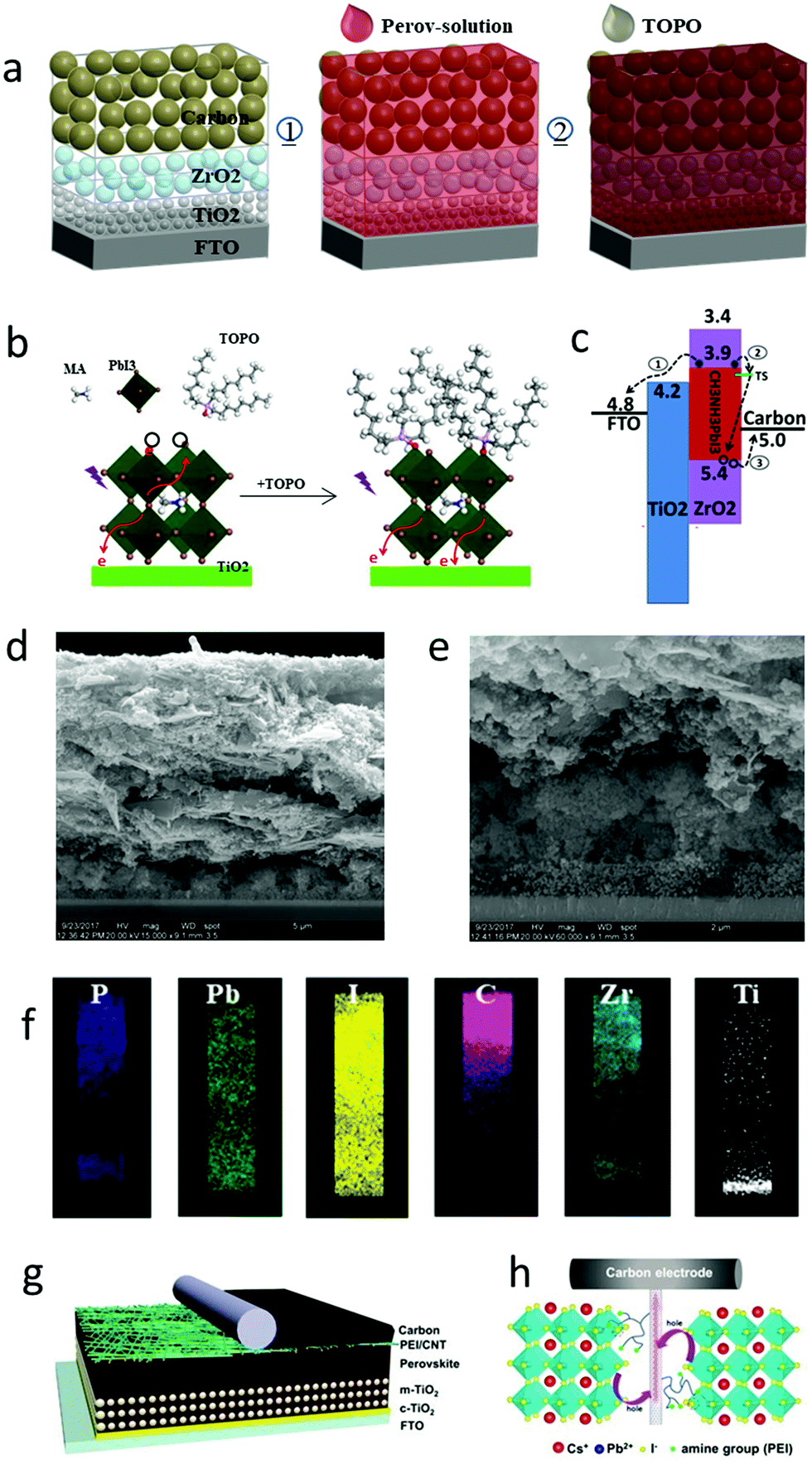 | ||
| Fig. 12 (a) Schematic of the fabrication of the TOPO capped carbon-based MPSCs. (b) The corresponding energy level of TiO2, perovskite, ZrO2 and carbon. The TS represents trap state. (c) Schematic of the interaction of the TOPO and perovskite defects. (d) Cross-sectional SEM image of TOPO capped meso C-PSCs. (e) The expanded TiO2/ZrO2 region in white solid frame. (f) Elemental distribution mapping images for the white dashed frame.180 Copyright 2018, Royal Society of Chemistry. (g) Device architecture of C-PSCs with implanted PEI/CNT bridging at the perovskite/carbon electrode interface. (h) Schematic of the charge transfer process from perovskite to carbon electrode via PEI/CNT as both the bridge and perovskite surface trap state passivation molecule.181 Copyright 2019, Royal Society of Chemistry. | ||
Yang et al. applied a polyethyleneimine-functionalized carbon nanotube (PEI/CNT) to the interface between the perovskite layer and the carbon electrode to improve the interface contact.181 PEI molecules also had the effect of passivating interface defects.181 It was found that PEI molecules were anchored on the perovskite framework by amino groups via the coordination interaction between –NH2 (–NH–) and Pb2+ or the hydrogen bond between H atoms in –NH2 (–NH–) and I−, thereupon passivating the surface trap state in CsPbI3.181 Due to the improvement of the contact between the perovskite/carbon interface, the charge transfer was accelerated. C-PSCs finally obtained 10.55% PCE and 0.71 FF.181Fig. 12(g) shows the specific structure of the device, and the existence of the PEI/CNT bridge could be observed.181 During the preparation of C-PSCs, the PEI/CNT bridge was deposited on the perovskite/carbon electrode interface and partially infiltrated in the perovskite layer, as shown in Fig. 12(h).181 CNTs were first oxidized by mixed acids (sulfuric acid and nitric acid), and then carboxyl groups were introduced into the surface of CNTs. Finally, PEI molecules were connected to CNTs by the dehydration reaction between carboxyl and amino groups.185 Hence, the PEI/CNT interface bridging method was expected to prepare efficient and stable C-PSCs.
4.4 Build-in electric field
Sandberg et al. studied whether the built-in electric field has an impact on the device efficiency.188 After measurements and analysis, it was found that the built-in electric field could achieve the effective extraction of carriers. As the carriers produced by the perovskite absorption layer diffuse across toward the carbon electrode side, they would leave behind negatively charged electrons near the interface between the perovskite layer and the carbon electrode regions. Then, the positively holes would diffuse to the carbon electrode. These charges form an electric field at the interface, and the free electrons and holes are affected by built-in electric field and flow in the opposite direction of diffusion.105,189–193Lee et al. revealed that increasing the difference in Wf between the carbon electrode and the perovskite layer could facilitate the driving force of carrier migration, which indicated that the built-in electric field was driven by the difference of Wf.194 The enhancement of the built-in electric field could not only promote the carrier migration, but also improve the hole collection of the carbon electrode and reduce the charge recombination.26,195,196
In 2014, Yan et al. found that multi-layer graphene (MG) as a counter electrode would produce a Schottky barrier at the interface with the perovskite layer, which greatly improved the efficiency of the device.186Fig. 13(a) and (b) exhibit the energy band diagrams of SG/perovskite and MG/perovskite, respectively. It can be found that there was a large Fermi level shift at the interface between multi-layer graphene and perovskite, forming a Schottky barrier. The MG had some conservative sandwich graphite layers in the oxidation process, so it had a good electrical conductivity. In addition, the mutual accumulation of MG could also fill the defects between each other (Fig. 13(c) and (d)). Most importantly, thanks to the built-in field of the Schottky junction, the hole extraction speed was enhanced and the interface charge recombination was greatly suppressed. They achieved a PCE of 11.5%. In 2019, He et al. used copper phthalocyanine (CuPc) to enhance the built-in electric field between the carbon electrode and the perovskite layer, and the efficiency increased to 14.8%.187 From the SEM images of Fig. 13(f) and (g), it could be seen that the morphology of the carbon electrode was not affected by CuPc. The device structure with CuPc carbon electrodes is shown in Fig. 13(e). Compared with the bare carbon electrode, the Wf value of the CuPc-doped carbon electrode increased from 4.03 eV to 4.22 eV (Fig. 13(h)). The increase in Wf difference led to the enhancement of built-in electric field at the interface between carbon electrode and perovskite layer, which improved JSC, VOC and FF values.
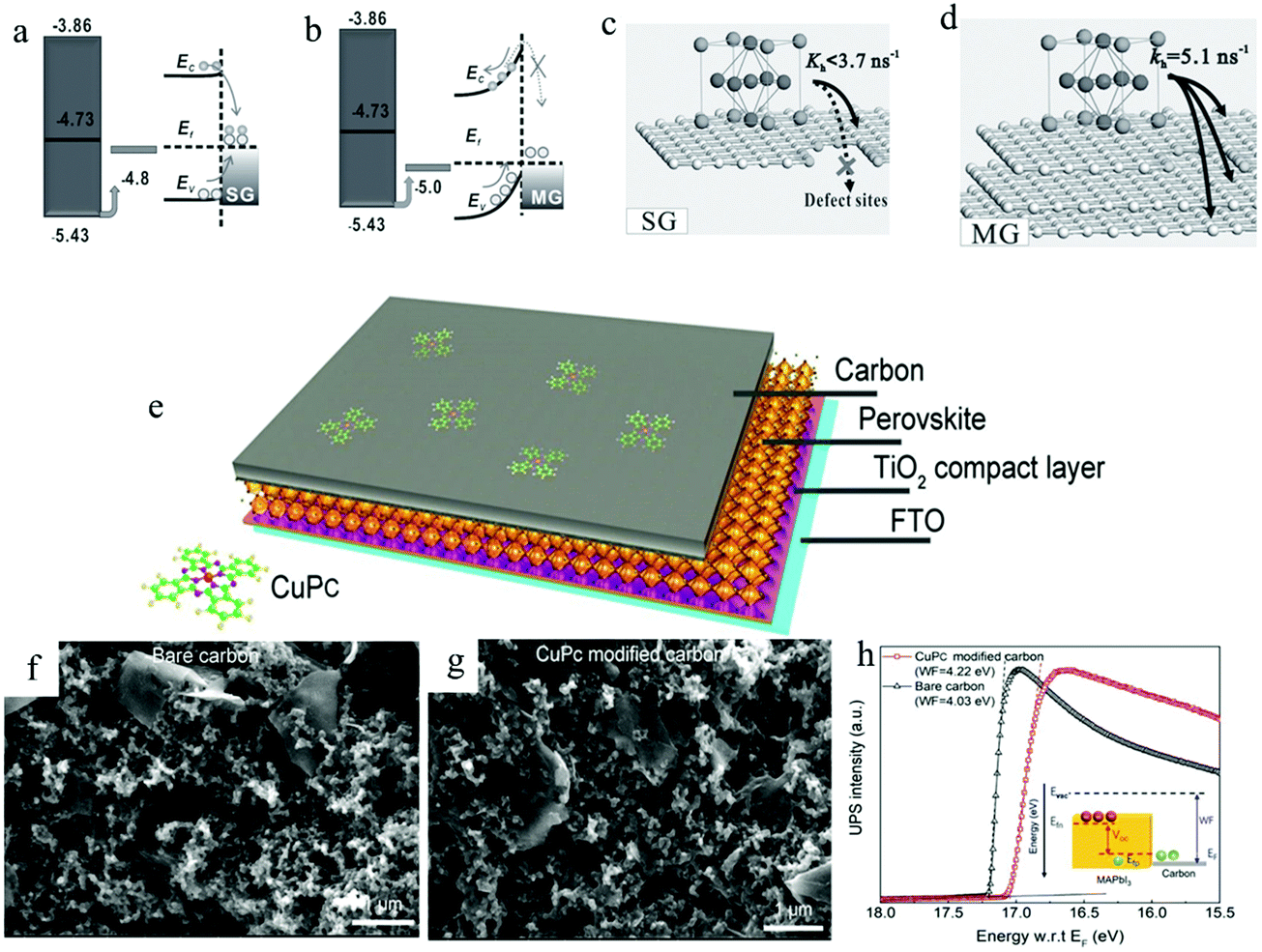 | ||
| Fig. 13 Schematic of (a) ohmic contact of single-layer graphene (SG)/perovskite with possible recombination and (b) Schottky junction of multi-layer graphene (MG)/perovskite with directional charge transfer. Schematic diagram of stronger hole extraction capability of MG (d) than SG (c).186 Copyright 2014, Wiley. (e) Schematic drawing showing the carbon electrode-based PSC structure. Surface SEM image of the carbon electrode without (f) and with (g) CuPc. (h) UPS spectra of the carbon electrode revealing Wf differences.187 Copyright 2019, American Chemical Society. | ||
In summary, through the latest progress of the four interface engineering of C-PSCs shown above, it can be seen that the effect of eliminating hysteresis is the best, and the other three are achieved by mixing other materials with carbon electrodes.64,197–202 Obviously, eliminating the hysteresis phenomenon is the most likely to update the highest efficiency of the carbon electrode.
5. Conclusion and outlooks
In this paper, the important outcomes of carbon-based PSCs were reviewed. The rear electrodes developed with carbon black, graphite, graphenes or carbon nanotubes show superior stability, thanks to the hydrophobicity of carbon materials. Researchers have developed several processing methods, from meso to embedment, as well as paintable C-PSCs. The research results of previous works show that the PCE of C-PSCs is still not comparable to that of M-PSCs. The main reason is the inferior interface contact between the perovskite and the carbon electrode. Second, the square resistance and charge recombination of carbon electrodes are also the reasons for the low values of JSC and FF. The currently reported solutions show that the interface engineering of C-PSCs has become a hot topic in the photovoltaic field. Scientists are trying to homogenize the photoelectronic properties of the perovskite and carbon electrodes and then passivate the interface defects to accelerate charge transfer and reduce recombination.To further improve the efficiency, the main challenge facing C-PSCs in the future is still the problem of interface contact. This problem stems from the inherent physical properties of carbon materials, e.g. crystal structure, size, electrical conductivity. Simultaneously, the morphology of the perovskite layer also has a great influence on the device. This can be improved through the following strategies. (i) The other materials (e.g. copper phthalocyanine, MXene) doped with carbon electrodes are used to accelerate charge transfer, enhance charge collection and reduce charge recombination. (ii) The high-quality perovskite films are prepared by a room temperature solvent exchange method, melt-assisted growth method and top seed method to reduce surface defects and improve interfacial contact. (iii) The interlayer (e.g. copper phthalocyanine and polyethyleneimine-functionalized) is added to the carbon electrode/perovskite interface with improving the work function, reducing the energy level mismatch and increasing the contact area.
The low-temperature carbon electrode discussed in the literature has good interfacial contact and a series of studies can be carried out. These are good research directions. Furthermore, based on the light absorption properties of carbon materials, the development of new characterization methods of C-PSCs is also a very important direction. This can increase the light absorption capacity of carbon materials, resulting in more electron–hole pairs and increased efficiency. Overall, there is much room to enhance their stability and efficiency for future practical applications.
Author contributions
Meidan Que: resources, writing reviewing and editing. Boyue Zhang: writing original draft preparation. Jin Chen: conceptualization. Xingtian Yin: conceptualization. Sining Yun: conceptualization.Conflicts of interest
The authors declare no competing financial interest. Further permissions related to the material excerpted from ref. 187 should be directed to the ACS.Acknowledgements
Funding for this work was provided by the National Natural Science Foundation of China (No. 62004155), Scientific Research Project of Shaanxi Provincial Department of Education (No. 20JK0714), Natural Science Special Project of Xi’an University of Architecture and Technology (ZR19031), and Independent Research and Development project of State Key Laboratory of Green Building in Western China (LSZZ202117).References
- A. Kojima, K. Teshima, Y. Shirai and T. Miyasaka, J. Am. Chem. Soc., 2009, 131, 6050–6051 CrossRef CAS PubMed.
- H. S. Kim, C. R. Lee, J. H. Im, K. B. Lee, T. Moehl, A. Marchioro, S. J. Moon, R. Humphry-Baker, J. H. Yum, J. E. Moser, M. Gratzel and N. G. Park, Sci. Rep., 2012, 2, 591 CrossRef.
- J. Burschka, N. Pellet, S. J. Moon, R. Humphry-Baker, P. Gao, M. K. Nazeeruddin and M. Gratzel, Nature, 2013, 499, 316–319 CrossRef CAS PubMed.
- J. H. Im, I. H. Jang, N. Pellet, M. Gratzel and N. G. Park, Nat. Nanotechnol., 2014, 9, 927–932 CrossRef CAS PubMed.
- M. Liu, M. B. Johnston and H. J. Snaith, Nature, 2013, 501, 395–398 CrossRef CAS.
- K. Yan, M. Long, T. Zhang, Z. Wei, H. Chen, S. Yang and J. Xu, J. Am. Chem. Soc., 2015, 137, 4460–4468 CrossRef CAS PubMed.
- T. Zhang, X. Meng, Y. Bai, S. Xiao, C. Hu, Y. Yang, H. Chen and S. Yang, J. Mater. Chem. A, 2017, 5, 1103–1111 RSC.
- G. Xing, N. Mathews, S. Sun, S. S. Lim, Y. M. Lam, M. Gratzel, S. Mhaisalkar and T. C. Sum, Science, 2013, 342, 344–347 CrossRef CAS.
- D. Shi, V. Adinolfl, R. Comin, M. Yuan, E. Alarousu, A. Buin, Y. Chen, S. Hoogland, A. Rothenberger, K. Katsiev, Y. Losovyj, X. Zhang, P. A. Dowben, O. F. Mohammed, E. H. Sargent and O. M. Bakr, Science, 2015, 347, 519–522 CrossRef CAS.
- C. S. Ponseca Jr, T. J. Savenije, M. Abdellah, K. Zheng, A. Yartsev, T. Pascher, T. Harlang, P. Chabera, T. Pullerits, A. Stepanov, J. P. Wolf and V. Sundstrom, J. Am. Chem. Soc., 2014, 136, 5189–5192 CrossRef.
- K.-G. Lim, S. Ahn, Y.-H. Kim, Y. Qi and T.-W. Lee, Energy Environ. Sci., 2016, 9, 932–939 RSC.
- Q. Dong, Y. Fang, Y. Shao, P. Mulligan, J. Qiu, L. Cao and J. Huang, Science, 2015, 347, 967–970 CrossRef CAS PubMed.
- V. D'Innocenzo, G. Grancini, M. J. Alcocer, A. R. Kandada, S. D. Stranks, M. M. Lee, G. Lanzani, H. J. Snaith and A. Petrozza, Nat. Commun., 2014, 5, 3586 CrossRef PubMed.
- S. Y. Sun, T. Salim, N. Mathews, M. Duchamp, C. Boothroyd, G. C. Xing, T. C. Sum and Y. M. Lam, Energy Environ. Sci., 2014, 7, 399–407 RSC.
- R. F. Service, Science, 2016, 354, 1214–1215 CrossRef CAS.
- D. Akin Kara, K. Kara, G. Oylumluoglu, M. Z. Yigit, M. Can, J. J. Kim, E. K. Burnett, D. L. Gonzalez Arellano, S. Buyukcelebi, F. Ozel, O. Usluer, A. L. Briseno and M. Kus, ACS Appl. Mater. Interfaces, 2018, 10, 30000–30007 CrossRef CAS.
- M. M. Lee, J. Teuscher, T. Miyasaka, T. N. Murakami and H. J. Snaith, Science, 2019, 338, 643–647 CrossRef.
- Laboratory, N.R.E., 2021, http://www.nrel.
- H. Chen and S. Yang, Adv. Mater., 2017, 29, 1603994 CrossRef.
- B. Vaagensmith, K. M. Reza, M. N. Hasan, H. Elbohy, N. Adhikari, A. Dubey, N. Kantack, E. Gaml and Q. Qiao, ACS Appl. Mater. Interfaces, 2017, 9, 35861–35870 CrossRef CAS.
- G. Martínez-Denegri, S. Colodrero, M. Kramarenko and J. Martorell, ACS Appl. Energy Mater., 2018, 1, 5548–5556 Search PubMed.
- M. I. Hossain, A. Hongsingthong, W. Qarony, P. Sichanugrist, M. Konagai, A. Salleo, D. Knipp and Y. H. Tsang, ACS Appl. Mater. Interfaces, 2019, 11, 14693–14701 CrossRef CAS PubMed.
- I. M. Hossain, D. Hudry, F. Mathies, T. Abzieher, S. Moghadamzadeh, D. Rueda-Delgado, F. Schackmar, M. Bruns, R. Andriessen, T. Aernouts, F. Di Giacomo, U. Lemmer, B. S. Richards, U. W. Paetzold and A. Hadipour, ACS Appl. Energy Mater., 2018, 2, 47–58 CrossRef.
- P. Tockhorn, J. Sutter, R. Colom, L. Kegelmann, A. Al-Ashouri, M. Roß, K. Jäger, T. Unold, S. Burger, S. Albrecht and C. Becker, ACS Photonics, 2020, 7, 2589–2600 CrossRef CAS.
- Z. Ku, Y. Rong, M. Xu, T. Liu and H. Han, Sci. Rep., 2013, 3, 3132 CrossRef PubMed.
- F. Zhang, X. Yang, H. Wang, M. Cheng, J. Zhao and L. Sun, ACS Appl. Mater. Interfaces, 2014, 6, 16140–16146 CrossRef CAS.
- Z. Liu, T. Shi, Z. Tang, B. Sun and G. Liao, Nanoscale, 2016, 8, 7017–7023 RSC.
- H. Zhang, J. Xiao, J. Shi, H. Su, Y. Luo, D. Li, H. Wu, Y.-B. Cheng and Q. Meng, Adv. Funct. Mater., 2018, 28, 1802985 CrossRef.
- H. W. Park, D. U. Lee, M. G. Park, R. Ahmed, M. H. Seo, L. F. Nazar and Z. Chen, ChemSusChem, 2015, 8, 1058–1065 CrossRef CAS.
- X. Meng, J. Zhou, J. Hou, X. Tao, S. H. Cheung, S. K. So and S. Yang, Adv. Mater., 2018, 30, e1706975 CrossRef PubMed.
- M. Chen, R.-H. Zha, Z.-Y. Yuan, Q.-S. Jing, Z.-Y. Huang, X.-K. Yang, S.-M. Yang, X.-H. Zhao, D.-L. Xu and G.-D. Zou, Chem. Eng. J., 2017, 313, 791–800 CrossRef CAS.
- C.-H. Lu, G. V. Biesold-McGee, Y. Liu, Z. Kang and Z. Lin, Chem. Soc. Rev., 2020, 49, 4953–5007 RSC.
- Z. Zong, B. He, J. Zhu, Y. Ding, W. Zhang, J. Duan, Y. Zhao, H. Chen and Q. Tang, Sol. Energy Mater. Sol. Cells, 2020, 209, 110460 CrossRef CAS.
- Y. Wang, J. Zhang, S. Chen, H. Zhang, L. Li and Z. Fu, J. Mater. Sci., 2018, 53, 9180–9190 CrossRef CAS.
- H. Chen and S. Yang, J. Mater. Chem. A, 2019, 7, 15476–15490 RSC.
- Y. Yue, N. Salim, Y. Wu, X. Yang, A. Islam, W. Chen, J. Liu, E. Bi, F. Xie, M. Cai and L. Han, Adv. Mater., 2016, 28, 10738–10743 CrossRef CAS.
- J. Ryu, K. Lee, J. Yun, H. Yu, J. Lee and J. Jang, Small, 2017, 13, 1701225 CrossRef PubMed.
- C. Ding, F. Liu, Y. Zhang, D. Hirotani, X. Rin, S. Hayase, T. Minemoto, T. Masuda, R. Wang and Q. Shen, Nano Energy, 2020, 67, 104267 CrossRef CAS.
- I.-G. Bae and B. Park, Sustainable Energy Fuels, 2020, 4, 3115–3128 RSC.
- J. Zhu, M. Tang, B. He, W. Zhang, X. Li, Z. Gong, H. Chen, Y. Duan and Q. Tang, J. Mater. Chem. A, 2020, 8, 20987–20997 RSC.
- X. Lin, D. Cui, X. Luo, C. Zhang, Q. Han, Y. Wang and L. Han, Energy Environ. Sci., 2020, 13, 3823–3847 RSC.
- J. A. Raiford, S. T. Oyakhire and S. F. Bent, Energy Environ. Sci., 2020, 13, 1997–2023 RSC.
- R. Nie, R. R. Sumukam, S. H. Reddy, M. Banavoth and S. I. Seok, Energy Environ. Sci., 2020, 13, 2363–2385 RSC.
- K. D. G. I. Jayawardena, S. M. Silva and R. K. Misra, J. Mater. Chem. C, 2020, 8, 10641–10675 RSC.
- N. Li, X. Niu, Q. Chen and H. Zhou, Chem. Soc. Rev., 2020, 49, 8235–8286 RSC.
- M. Aftabuzzaman, C. Lu and H. K. Kim, Nanoscale, 2020, 12, 17590–17648 RSC.
- D. Bogachuk, S. Zouhair, K. Wojciechowski, B. Yang, V. Babu, L. Wagner, B. Xu, J. Lim, S. Mastroianni, H. Pettersson, A. Hagfeldt and A. Hinsch, Energy Environ. Sci., 2020, 13, 3880–3916 RSC.
- S. Gong, H. Li, Z. Chen, C. Shou, M. Huang and S. Yang, ACS Appl. Mater. Interfaces, 2020, 12, 34882–34889 CrossRef CAS.
- H. P. Boehm, Carbon, 1994, 13, 759–769 CrossRef.
- S. K. Hazra, S. Ghosh and T. K. Nandi, Appl. Therm. Eng., 2019, 163, 114402 CrossRef CAS.
- N. Cheng, P. Liu, F. Qi, Y. Xiao, W. Yu, Z. Yu, W. Liu, S.-S. Guo and X.-Z. Zhao, J. Power Sources, 2016, 332, 24–29 CrossRef CAS.
- H. Wei, J. Xiao, Y. Yang, S. Lv, J. Shi, X. Xu, J. Dong, Y. Luo, D. Li and Q. Meng, Carbon, 2015, 93, 861–868 CrossRef CAS.
- F. R. Li, Y. Xu, W. Chen, S. H. Xie and J. Y. Li, J. Mater. Chem. A, 2017, 5, 10374–10379 RSC.
- J. H. Im, J. Luo, M. Franckevicius, N. Pellet, P. Gao, T. Moehl, S. M. Zakeeruddin, M. K. Nazeeruddin, M. Gratzel and N. G. Park, Nano Lett., 2015, 15, 2120–2126 CrossRef CAS.
- Z. Zhuang, L. Qiu, L. Dong, Y. Chen, Z. Chu, X. Ma, P. Du and J. Xiong, Polym. Compos., 2020, 41, 2145–2153 CrossRef CAS.
- Z. Wei, K. Yan, H. Chen, Y. Yi, T. Zhang, X. Long, J. Li, L. Zhang, J. Wang and S. Yang, Energy Environ. Sci., 2014, 7, 3326–3333 RSC.
- B. Huang, G. Kong, E. N. Esfahani, S. Chen, Q. Li, J. Yu, N. Xu, Y. Zhang, S. Xie, H. Wen, P. Gao, J. Zhao and J. Li, npj Quantum Mater., 2018, 3 DOI:10.1038/s41535-018-0104-5.
- D. Bai, H. Bian, Z. Jin, H. Wang, L. Meng, Q. Wang and S. Liu, Nano Energy, 2018, 52, 408–415 CrossRef CAS.
- Y. Guo, X. Yin, J. Liu and W. Que, J. Mater. Chem. A, 2019, 7, 19008–19016 RSC.
- Z. Wang, X. Liu, Y. Lin, Y. Liao, Q. Wei, H. Chen, J. Qiu, Y. Chen and Y. Zheng, J. Mater. Chem. A, 2019, 7, 2773–2779 RSC.
- Y. Fan, J. Fang, X. Chang, M.-C. Tang, D. Barrit, Z. Xu, Z. Jiang, J. Wen, H. Zhao, T. Niu, D.-M. Smilgies, S. Jin, Z. Liu, E. Q. Li, A. Amassian, S. Liu and K. Zhao, Joule, 2019, 3, 2485–2502 CrossRef CAS.
- J. K. Nam, M. S. Jung, S. U. Chai, Y. J. Choi, D. Kim and J. H. Park, J. Phys. Chem. Lett., 2017, 8, 2936–2940 CrossRef CAS.
- Q.-Q. Chu, Z. Sun, B. Ding, K.-S. Moon, G.-J. Yang and C.-P. Wong, Nano Energy, 2020, 77, 105110 CrossRef CAS.
- Z. Wei, H. Chen, K. Yan, X. Zheng and S. Yang, J. Mater. Chem. A, 2015, 3, 24226–24231 RSC.
- M. Duan, Y. Rong, A. Mei, Y. Hu, Y. Sheng, Y. Guan and H. Han, Carbon, 2017, 120, 71–76 CrossRef CAS.
- C. Zhang, S. Wang, H. Zhang, Y. Feng, W. Tian, Y. Yan, J. Bian, Y. Wang, S. Jin, S. M. Zakeeruddin, M. Grätzel and Y. Shi, Energy Environ. Sci., 2019, 12, 3585–3594 RSC.
- X. Hu, H. Jiang, J. Li, J. Ma, D. Yang, Z. Liu, F. Gao and S. F. Liu, Nanoscale, 2017, 9, 8274–8280 RSC.
- K. Ahmad and S. M. Mobin, New J. Chem., 2017, 41, 14253–14258 RSC.
- J. H. Heo, D. H. Shin, D. H. Song, D. H. Kim, S. J. Lee and S. H. Im, J. Mater. Chem. A, 2018, 6, 8251–8258 RSC.
- Q.-D. Yang, J. Li, Y. Cheng, H.-W. Li, Z. Guan, B. Yu and S.-W. Tsang, J. Mater. Chem. A, 2017, 5, 9852–9858 RSC.
- S. Suragtkhuu, O. Tserendavag, U. Vandandoo, A. S. R. Bati, M. Bat-Erdene, J. G. Shapter, M. Batmunkh and S. Davaasambuu, RSC Adv., 2020, 10, 9133–9139 RSC.
- V. Babu, R. F. Pineda, T. Ahmad, A. Alvarez, L. A. Castriotta, A. D. Carlo, F. Fabregat-Santiago and K. Wojciechowski, ACS Appl. Energy Mater., 2020, 3, 5126–5134 CrossRef CAS.
- P. You, Z. Liu, Q. Tai, S. Liu and F. Yan, Adv. Mater., 2015, 27, 3632–3638 CrossRef CAS.
- H. Sung, N. Ahn, M. S. Jang, J.-K. Lee, H. Yoon, N.-G. Park and M. Choi, Adv. Energy Mater., 2016, 6, 1501873 CrossRef.
- J. H. Heo, D. H. Shin, S. Kim, M. H. Jang, M. H. Lee, S. W. Seo, S.-H. Choi and S. H. Im, Chem. Eng. J., 2017, 323, 153–159 CrossRef CAS.
- R. Ishikawa, S. Watanabe, S. Yamazaki, T. Oya and N. Tsuboi, ACS Appl. Energy Mater., 2019, 2, 171–175 CrossRef CAS.
- G. Mazzotta, M. Dollmann, S. N. Habisreutinger, M. G. Christoforo, Z. Wang, H. J. Snaith, M. K. Riede and R. J. Nicholas, ACS Appl. Mater. Interfaces, 2019, 11, 1185–1191 CrossRef CAS.
- Q. Luo, H. Ma, Q. Hou, Y. Li, J. Ren, X. Dai, Z. Yao, Y. Zhou, L. Xiang, H. Du, H. He, N. Wang, K. Jiang, H. Lin, H. Zhang and Z. Guo, Adv. Funct. Mater., 2018, 28, 1706777 CrossRef.
- I. Jeon, A. Shawky, S. Seo, Y. Qian, A. Anisimov, E. I. Kauppinen, Y. Matsuo and S. Maruyama, J. Mater. Chem. A, 2020, 8, 11141–11147 RSC.
- R. Wu, Q. Luo, L. Ma, C. Wang, H. Liu, H. Lin, N. Wang, Y. Chen and Z. Guo, Adv. Funct. Mater., 2020, 31, 2004765 Search PubMed.
- M. K. A. Mohammed, RSC Adv., 2020, 10, 35831–35839 RSC.
- S. Seo, I. Jeon, R. Xiang, C. Lee, H. Zhang, T. Tanaka, J.-W. Lee, D. Suh, T. Ogamoto, R. Nishikubo, A. Saeki, S. Chiashi, J. Shiomi, H. Kataura, H. M. Lee, Y. Yang, Y. Matsuo and S. Maruyama, J. Mater. Chem. A, 2019, 7, 12987–12992 RSC.
- X. Wu, L. Xie, K. Lin, J. Lu, K. Wang, W. Feng, B. Fan, P. Yin and Z. Wei, J. Mater. Chem. A, 2019, 7, 12236–12243 RSC.
- N. Ahn, I. Jeon, J. Yoon, E. I. Kauppinen, Y. Matsuo, S. Maruyama and M. Choi, J. Mater. Chem. A, 2018, 6, 1382–1389 RSC.
- Q. Luo, H. Ma, Y. Zhang, X. Yin, Z. Yao, N. Wang, J. Li, S. Fan, K. Jiang and H. Lin, J. Mater. Chem. A, 2016, 4, 5569–5577 RSC.
- R. B. K. Siram, M. V. Khenkin, A. Niazov-Elkan, K. M. Anoop, H. Weissman, E. A. Katz, I. Visoly-Fisher and B. Rybtchinski, Nanoscale, 2019, 11, 3733–3740 RSC.
- R. Belchi, B. Pibaleau, M. Pinault, B. Ratier, N. Herlin-Boime and J. Bouclé, Mater. Adv., 2020, 1, 1232–1240 RSC.
- C. Ma, S. Clark, Z. Liu, L. Liang, Y. Firdaus, R. Tao, A. Han, X. Liu, L. J. Li, T. D. Anthopoulos, M. C. Hersam and T. Wu, ACS Nano, 2020, 14, 3969–3979 CrossRef CAS PubMed.
- Q. Luo, H. Ma, F. Hao, Q. Hou, J. Ren, L. Wu, Z. Yao, Y. Zhou, N. Wang, K. Jiang, H. Lin and Z. Guo, Adv. Funct. Mater., 2017, 27, 1703068 CrossRef.
- K. Aitola, K. Sveinbjörnsson, J.-P. Correa-Baena, A. Kaskela, A. Abate, Y. Tian, E. M. J. Johansson, M. Grätzel, E. I. Kauppinen, A. Hagfeldt and G. Boschloo, Energy Environ. Sci., 2016, 9, 461–466 RSC.
- H. Zhou, Q. Chen, G. Li, S. Luo, T.-B. Song, H.-S. Duan, Z. Hong, J. You, Y. Liu and Y. Yang, Science, 2017, 345, 542–546 CrossRef PubMed.
- J. H. N. W. S. Yang, N. J. Jeon, Y. C. Kim, J. S. S. Ryu and S. Il Seok, Science, 2018, 348, 1234–1237 CrossRef PubMed.
- M. Saliba, K. Domanski, J.-Y. Seo, A. Ummadisingu, S. M. Zakeeruddin, J.-P. Correa-Baena, W. R. Tress, A. Abate, A. Hagfeldt and M. Grätzel, Science, 2018, 354, 206–209 CrossRef PubMed.
- W. S. Yang, E. H. Jung, N. J. Jeon, Y. C. Kim, D. U. Lee, S. S. Shin, J. Seo, E. K. Kim, J. H. Noh and S. Il Seok, Science, 2017, 356, 1376–1379 CrossRef CAS.
- N. J. Jeon, H. Na, E. H. Jung, T.-Y. Yang, Y. G. Lee, G. Kim, H.-W. Shin, S. Il Seok, J. Lee and J. Seo, Nat. Energy, 2018, 3, 682–689 CrossRef CAS.
- Q. Jiang, Y. Zhao, X. Zhang, X. Yang, Y. Chen, Z. Chu, Q. Ye, X. Li, Z. Yin and J. You, Nat. Photonics, 2019, 13, 460–466 CrossRef CAS.
- J. J. Yoo, G. Seo, M. R. Chua, T. G. Park, Y. Lu, F. Rotermund, Y. K. Kim, C. S. Moon, N. J. Jeon, J. P. Correa-Baena, V. Bulovic, S. S. Shin, M. G. Bawendi and J. Seo, Nature, 2021, 590, 587–593 CrossRef CAS.
- A. Mei, X. Li, L. Liu, Z. Ku, T. Liu, Y. Rong, M. Xu, M. Hu, J. Chen, Y. Yang, M. Gratzel and H. Han, Science, 2014, 345, 295–298 CrossRef CAS PubMed.
- Y. Yang, K. Ri, A. Mei, L. Liu, M. Hu, T. Liu, X. Li and H. Han, J. Mater. Chem. A, 2015, 3, 9103–9107 RSC.
- J. Chen, Y. Xiong, Y. Rong, A. Mei, Y. Sheng, P. Jiang, Y. Hu, X. Li and H. Han, Nano Energy, 2016, 27, 130–137 CrossRef CAS.
- H. Zhang, H. Wang, S. T. Williams, D. Xiong, W. Zhang, C. C. Chueh, W. Chen and A. K. Jen, Adv. Mater., 2017, 29, 1606608 CrossRef PubMed.
- S. Shukla, T. M. Koh, R. Patidar, J. H. Lew, P. Kajal, S. G. Mhaisalkar and N. Mathews, J. Phys. Chem. C, 2021, 125, 6585–6592 CrossRef CAS.
- Z. Wei, H. Chen, K. Yan and S. Yang, Angew. Chem., Int. Ed., 2014, 53, 13239–13243 CrossRef CAS PubMed.
- X. Zheng, H. Chen, Q. Li, Y. Yang, Z. Wei, Y. Bai, Y. Qiu, D. Zhou, K. S. Wong and S. Yang, Nano Lett., 2017, 17, 2496–2505 CrossRef CAS PubMed.
- Y. Yang, Z. Liu, W. K. Ng, L. Zhang, H. Zhang, X. Meng, Y. Bai, S. Xiao, T. Zhang, C. Hu, K. S. Wong and S. Yang, Adv. Funct. Mater., 2019, 29, 1806506 CrossRef.
- H. Chen, Z. Wei, H. He, X. Zheng, K. S. Wong and S. Yang, Adv. Energy Mater., 2016, 6, 1502087 CrossRef.
- K. Lee, J. Kim, H. Yu, J. W. Lee, C.-M. Yoon, S. K. Kim and J. Jang, J. Mater. Chem. A, 2018, 6, 24560–24568 RSC.
- S. Wang, P. Jiang, W. Shen, A. Mei, S. Xiong, X. Jiang, Y. Rong, Y. Tang, Y. Hu and H. Han, Chem. Commun., 2019, 55, 2765–2768 RSC.
- Y. Cao, W. Li, Z. Liu, Z. Zhao, Z. Xiao, W. Zi and N. Cheng, J. Mater. Chem. A, 2020, 8, 12080–12088 RSC.
- P. Mariani, L. Najafi, G. Bianca, M. I. Zappia, L. Gabatel, A. Agresti, S. Pescetelli, A. Di Carlo, S. Bellani and F. Bonaccorso, ACS Appl. Mater. Interfaces, 2021, 13, 22368–22380 CrossRef CAS PubMed.
- Y. Rong, Z. Ku, A. Mei, T. Liu, M. Xu, S. Ko, X. Li and H. Han, J. Phys. Chem. Lett., 2014, 5, 2160–2164 CrossRef CAS PubMed.
- L. Zhang, T. Liu, L. Liu, M. Hu, Y. Yang, A. Mei and H. Han, J. Mater. Chem. A, 2015, 3, 9165–9170 RSC.
- M. Xu, Y. Rong, Z. Ku, A. Mei, T. Liu, L. Zhang, X. Li and H. Han, J. Mater. Chem. A, 2014, 2, 8607–8611 RSC.
- A. K. Baranwal, S. Kanaya, T. A. Peiris, G. Mizuta, T. Nishina, H. Kanda, T. Miyasaka, H. Segawa and S. Ito, ChemSusChem, 2016, 9, 2604–2608 CrossRef CAS PubMed.
- E. V. Péan, C. S. De Castro, S. Dimitrov, F. De Rossi, S. Meroni, J. Baker, T. Watson and M. L. Davies, Adv. Funct. Mater., 2020, 30, 1909839 CrossRef.
- S. Wang, W. Shen, Y. Chu, W. Zhang, L. Hong, A. Mei, Y. Rong, Y. Tang, Y. Hu and H. Han, J. Phys. Chem. Lett., 2020, 11, 9689–9695 CrossRef CAS PubMed.
- R. Kerremans, O. J. Sandberg, S. Meroni, T. Watson, A. Armin and P. Meredith, Sol. RRL, 2019, 4, 1900221 CrossRef.
- J. Baker, K. Hooper, S. Meroni, A. Pockett, J. McGettrick, Z. Wei, R. Escalante, G. Oskam, M. Carnie and T. Watson, J. Mater. Chem. A, 2017, 5, 18643–18650 RSC.
- D. Raptis, V. Stoichkov, S. M. P. Meroni, A. Pockett, C. A. Worsley, M. Carnie, D. A. Worsley and T. Watson, Curr. Appl. Phys., 2020, 20, 619–627 CrossRef.
- A. Pockett, D. Raptis, S. M. P. Meroni, J. Baker, T. Watson and M. Carnie, J. Phys. Chem. C, 2019, 123, 11414–11421 CrossRef CAS.
- D. Papadatos, D. Sygkridou and E. Stathatos, Mater. Lett., 2020, 268, 127621 CrossRef CAS.
- J. Ryu, S. Yoon, J. Park, S. M. Jeong and D.-W. Kang, Appl. Surf. Sci., 2020, 516, 146116 CrossRef CAS.
- T. Ye, X. Jiang, D. Wan, X. Wang, J. Xing, T. Venkatesan, Q. Xiong and S. Ramakrishna, Chem. Phys. Chem., 2016, 17, 4102–4109 CrossRef CAS PubMed.
- I. Onwubiko, W. S. Khan, B. Subeshan and R. Asmatulu, Energy Ecol. Environ., 2020, 5, 141–152 CrossRef.
- Q.-Q. Chu, B. Ding, Y. Li, L. L. Gao, Q. Qiu, C.-X. Li, C.-J. Li, G.-J. Yang and B. Fang, ACS Sustainable Chem. Eng., 2017, 5, 9758–9765 CrossRef CAS.
- Y. Wang, H. Zhao, Y. Mei, H. Liu, S. Wang and X. Li, ACS Appl. Mater. Interfaces, 2019, 11, 916–923 CrossRef CAS PubMed.
- H. Chen and S. Yang, J. Mater. Res., 2017, 32, 3011–3020 CrossRef CAS.
- Y. Yang, J. Xiao, H. Wei, L. Zhu, D. Li, Y. Luo, H. Wu and Q. Meng, RSC Adv., 2014, 4, 52825–52830 RSC.
- C. Lee, S.-W. Lee, S. Bae, A. Shawky, V. Devaraj, A. Anisimov, E. I. Kauppinen, J.-W. Oh, Y. Kang, D. Kim, I. Jeon, S. Maruyama and H.-S. Lee, Sol. RRL, 2020, 4, 2000353 CrossRef CAS.
- I. Jeon, J. Yoon, U. Kim, C. Lee, R. Xiang, A. Shawky, J. Xi, J. Byeon, H. M. Lee, M. Choi, S. Maruyama and Y. Matsuo, Adv. Energy Mater., 2019, 9, 1901204 CrossRef.
- Z. Wei, X. Zheng, H. Chen, X. Long, Z. Wang and S. Yang, J. Mater. Chem. A, 2015, 3, 16430–16434 RSC.
- Y. Hu, Z. Zhang, A. Mei, Y. Jiang, X. Hou, Q. Wang, K. Du, Y. Rong, Y. Zhou, G. Xu and H. Han, Adv. Mater., 2018, 30, 1705786 CrossRef PubMed.
- S.-H. Turren-Cruz, M. Saliba, M. T. Mayer, H. Juárez-Santiesteban, X. Mathew, L. Nienhaus, W. Tress, M. P. Erodici, M.-J. Sher, M. G. Bawendi, M. Grätzel, A. Abate, A. Hagfeldt and J.-P. Correa-Baena, Energy Environ. Sci., 2018, 11, 78–86 RSC.
- M. Batmunkh, T. J. Macdonald, C. J. Shearer, M. Bat-Erdene, Y. Wang, M. J. Biggs, I. P. Parkin, T. Nann and J. G. Shapter, Adv. Sci., 2017, 4, 1600504 CrossRef PubMed.
- F. Tan, M. I. Saidaminov, H. Tan, J. Z. Fan, Y. Wang, S. Yue, X. Wang, Z. Shen, S. Li, J. Kim, Y. Gao, G. Yue, R. Liu, Z. Huang, C. Dong, X. Hu, W. Zhang, Z. Wang, S. Qu, Z. Wang and E. H. Sargent, Adv. Funct. Mater., 2020, 30, 2005155 CrossRef CAS.
- F. Deng, X. Sun, X. Lv, Y. Li and X. Tao, J. Power Sources, 2021, 489, 229345 CrossRef CAS.
- M. Duan, C. Tian, Y. Hu, A. Mei, Y. Rong, Y. Xiong, M. Xu, Y. Sheng, P. Jiang, X. Hou, X. Zhu, F. Qin and H. Han, ACS Appl. Mater. Interfaces, 2017, 9, 31721–31727 CrossRef CAS PubMed.
- Y. Sheng, A. Mei, S. Liu, M. Duan, P. Jiang, C. Tian, Y. Xiong, Y. Rong, H. Han and Y. Hu, J. Mater. Chem. A, 2018, 6, 2360–2364 RSC.
- F. Zhang, X. Yang, M. Cheng, J. Li, W. Wang, H. Wang and L. Sun, J. Mater. Chem. A, 2015, 3, 24272–24280 RSC.
- Y. Xiong, Y. Liu, K. Lan, A. Mei, Y. Sheng, D. Zhao and H. Han, New J. Chem., 2018, 42, 2669–2674 RSC.
- Y. Rong, X. Hou, Y. Hu, A. Mei, L. Liu, P. Wang and H. Han, Nat. Commun., 2017, 8, 14555 CrossRef PubMed.
- C. Raminafshar, V. Dracopoulos, M. R. Mohammadi and P. Lianos, Electrochim. Acta, 2018, 276, 261–267 CrossRef CAS.
- X. Xu, Z. Liu, Z. Zuo, M. Zhang, Z. Zhao, Y. Shen, H. Zhou, Q. Chen, Y. Yang and M. Wang, Nano Lett., 2015, 15, 2402–2408 CrossRef CAS PubMed.
- C. Tian, A. Mei, S. Zhang, H. Tian, S. Liu, F. Qin, Y. Xiong, Y. Rong, Y. Hu, Y. Zhou, S. Xie and H. Han, Nano Energy, 2018, 53, 160–167 CrossRef CAS.
- H. Tao, Y. Li, C. Zhang, K. Wang, J. Wang, B. Tan, L. Han and J. Tao, Solid State Commun., 2018, 271, 71–75 CrossRef CAS.
- F. Behrouznejad, C. M. Tsai, S. Narra, E. W. Diau and N. Taghavinia, ACS Appl. Mater. Interfaces, 2017, 9, 25204–25215 CrossRef CAS PubMed.
- P. Jiang, Y. Xiong, M. Xu, A. Mei, Y. Sheng, L. Hong, T. W. Jones, G. J. Wilson, S. Xiong, D. Li, Y. Hu, Y. Rong and H. Han, J. Phys. Chem. C, 2018, 122, 16481–16487 CrossRef CAS.
- F. Zhang, X. Yang, M. Cheng, W. Wang and L. Sun, Nano Energy, 2016, 20, 108–116 CrossRef CAS.
- R. Hu, R. Zhang, Y. Ma, W. Liu, L. Chu, W. Mao, J. Zhang, J. Yang, Y. Pu and X. A. Li, Appl. Surf. Sci., 2018, 462, 840–846 CrossRef CAS.
- H. Ye, Z. Liu, X. Liu, B. Sun, X. Tan, Y. Tu, T. Shi, Z. Tang and G. Liao, Appl. Surf. Sci., 2019, 478, 417–425 CrossRef CAS.
- H. Liu, X. Fu, W. Fu, B. Zong, L. Huang, H. Bala, S. Wang, Z. Guo, G. Sun, J. Cao and Z. Zhang, Org. Electron., 2018, 59, 253–259 CrossRef CAS.
- J. Chen and N.-G. Park, ACS Energy Lett., 2020, 5, 2742–2786 CrossRef CAS.
- A. Bashir, S. Shukla, J. H. Lew, S. Shukla, A. Bruno, D. Gupta, T. Baikie, R. Patidar, Z. Akhter, A. Priyadarshi, N. Mathews and S. G. Mhaisalkar, Nanoscale, 2018, 10, 2341–2350 RSC.
- R. L. Davidovich, V. Stavila, D. V. Marinin, E. I. Voit and K. H. Whitmire, Coord. Chem. Rev., 2009, 253, 1316–1352 CrossRef CAS.
- G. Mahmoudi, A. Bauza and A. Frontera, Dalton Trans., 2016, 45, 4965–4969 RSC.
- K. Dasgupta and D. Sathiyamoorthy, Mater. Sci. Technol., 2013, 19, 995–1002 CrossRef.
- S. Stankovich, D. A. Dikin, R. D. Piner, K. A. Kohlhaas, A. Kleinhammes, Y. Jia, Y. Wu, S. T. Nguyen and R. S. Ruoff, Carbon, 2007, 45, 1558–1565 CrossRef CAS.
- S.-S. Li, K.-H. Tu, C.-C. Lin, C.-W. Chen and M. Chhowalla, ACS Nano, 2010, 4, 3169–3174 CrossRef CAS PubMed.
- C. Mattevi, G. Eda, S. Agnoli, S. Miller, K. A. Mkhoyan, O. Celik, D. Mastrogiovanni, G. Granozzi, E. Garfunkel and M. Chhowalla, Adv. Funct. Mater., 2009, 19, 2577–2583 CrossRef CAS.
- H. S. Kim and N. G. Park, J. Phys. Chem. Lett., 2014, 5, 2927–2934 CrossRef CAS PubMed.
- W. Tress, J. P. Correa Baena, M. Saliba, A. Abate and M. Graetzel, Adv. Energy Mater., 2016, 6, 1600396 CrossRef.
- C. Xia, W.-D. Song, C.-Z. Zhang, S.-Y. Yuan, W.-X. Hu, P. Qin, R.-P. Wang, L.-L. Zhao, X.-F. Wang, M. He and S.-T. Li, Chin. Phys. B, 2017, 26, 018401 CrossRef.
- M. F. Ayguler, A. G. Hufnagel, P. Rieder, M. Wussler, W. Jaegermann, T. Bein, V. Dyakonov, M. L. Petrus, A. Baumann and P. Docampo, ACS Appl. Mater. Interfaces, 2018, 10, 11414–11419 CrossRef PubMed.
- J. Y. Kim, J. W. Lee, H. S. Jung, H. Shin and N. G. Park, Chem. Rev., 2020, 120, 7867–7918 CrossRef CAS PubMed.
- S. Mashhoun, Y. Hou, H. Chen, F. Tajabadi, N. Taghavinia, H.-J. Egelhaaf and C. J. Brabec, Adv. Energy Mater., 2018, 8, 1802085 CrossRef.
- L. Fagiolari and F. Bella, Energy Environ. Sci., 2019, 12, 3437–3472 RSC.
- B. Chen, M. Yang, S. Priya and K. Zhu, J. Phys. Chem. Lett., 2016, 7, 905–917 CrossRef CAS PubMed.
- S. N. Habisreutinger, N. K. Noel and H. J. Snaith, ACS Energy Lett., 2018, 3, 2472–2476 CrossRef CAS.
- P. Calado, A. M. Telford, D. Bryant, X. Li, J. Nelson, B. C. O'Regan and P. R. Barnes, Nat. Commun., 2016, 7, 13831 CrossRef CAS PubMed.
- Y. Zhou, F. Huang, Y.-B. Cheng and A. Gray-Weale, Comput. Mater. Sci., 2017, 126, 22–28 CrossRef CAS.
- S. Ravishankar, S. Gharibzadeh, C. Roldán-Carmona, G. Grancini, Y. Lee, M. Ralaiarisoa, A. M. Asiri, N. Koch, J. Bisquert and M. K. Nazeeruddin, Joule, 2018, 2, 788–798 CrossRef CAS.
- S. A. L. Weber, I. M. Hermes, S.-H. Turren-Cruz, C. Gort, V. W. Bergmann, L. Gilson, A. Hagfeldt, M. Graetzel, W. Tress and R. Berger, Energy Environ. Sci., 2018, 11, 2404–2413 RSC.
- H. J. Snaith, A. Abate, J. M. Ball, G. E. Eperon, T. Leijtens, N. K. Noel, S. D. Stranks, J. T. Wang, K. Wojciechowski and W. Zhang, J. Phys. Chem. Lett., 2014, 5, 1511–1515 CrossRef CAS PubMed.
- J. Park, S. E. Yoon, J. Lee, D. R. Whang, S. Y. Lee, S. J. Shin, J. M. Han, H. Seo, H. J. Park, J. H. Kim and B. G. Kim, Adv. Funct. Mater., 2020, 30, 2001560 CrossRef CAS.
- X. Wang, L. Zhi and K. Mullen, Nano Lett., 2008, 8, 323–327 CrossRef CAS PubMed.
- L. G. De Arco, Y. Zhang, C. W. Schlenker, K. Ryu, M. E. Thompson and C. Zhou, ACS Nano, 2010, 4, 2865–2873 CrossRef PubMed.
- H. Park, P. R. Brown, V. Bulović and J. Kong, Nano Lett., 2011, 12, 133–140 CrossRef PubMed.
- Z. Yin, J. Zhu, Q. He, X. Cao, C. Tan, H. Chen, Q. Yan and H. Zhang, Adv. Energy Mater., 2014, 4, 1300574 CrossRef.
- R. Singh, P. K. Singh, B. Bhattacharya and H.-W. Rhee, Appl. Mater. Today, 2019, 14, 175–200 CrossRef.
- G. Huang, C. Wang, H. Zhang, S. Xu, Q. Xu and Y. Cui, J. Mater. Chem. A, 2018, 6, 2449–2455 RSC.
- Y. Yang, H. Chen, C. Hu and S. Yang, J. Mater. Chem. A, 2019, 7, 22005–22011 RSC.
- S. Liu, L. Guan, T. Zhang, X. Gong, X. Zhao, Q. Sun, X. Shai, X. L. Zhang, X. Xiao, Y. Shen and M. Wang, Appl. Mater. Today, 2020, 20, 100644 CrossRef.
- M. Abd Mutalib, F. Aziz, A. F. Ismail, W. N. Wan Salleh, N. Yusof, J. Jaafar, T. Soga, M. Z. Sahdan and N. Ahmad Ludin, Appl. Mater. Today, 2018, 13, 69–82 CrossRef.
- M.-y. Li, H. Yin and G.-Y. Sun, Appl. Mater. Today, 2020, 21, 100799 CrossRef.
- W. Chidawanyika and T. Nyokong, Carbon, 2010, 48, 2831–2838 CrossRef CAS.
- K. Yan, Z. Wei, J. Li, H. Chen, Y. Yi, X. Zheng, X. Long, Z. Wang, J. Wang, J. Xu and S. Yang, Small, 2015, 11, 2269–2274 CrossRef CAS PubMed.
- S. He, L. Qiu, D.-Y. Son, Z. Liu, E. J. Juarez-Perez, L. K. Ono, C. Stecker and Y. Qi, ACS Energy Lett., 2019, 4, 2032–2039 CrossRef CAS.
- O. J. Sandberg, J. Kurpiers, M. Stolterfoht, D. Neher, P. Meredith, S. Shoaee and A. Armin, Adv. Mater. Interfaces, 2020, 7, 2000041 CrossRef CAS.
- http://www.bookshop.unsw.edu.au .
- W. A. Laban and L. Etgar, Energy Environ. Sci., 2013, 6, 3249–3253 RSC.
- L. Cai, Y. Wang, N. Li, A. A. Syed and F. Zhu, Energy Technol., 2020, 8, 2000192 CrossRef CAS.
- J. Wu, Y. Li, S. Tan, B. Yu, H. Li, Y. Li, J. Shi, H. Wu, Y. Luo, D. Li and Q. Meng, ACS Appl. Mater. Interfaces, 2020, 12, 27258–27267 CrossRef CAS PubMed.
- H. Chen and S. Yang, Sci. Bull., 2016, 61, 1680–1688 CrossRef CAS.
- J.-H. Lee, J. Kim, G. Kim, D. Shin, S. Y. Jeong, J. Lee, S. Hong, J. W. Choi, C.-L. Lee, H. Kim, Y. Yi and K. Lee, Energy Environ. Sci., 2018, 11, 1742–1751 RSC.
- Z. Liu, X. Yu and L. Li, Chin. J. Catal., 2020, 41, 534–549 CrossRef CAS.
- W. T. Wang, P. Chen, C. H. Chiang, T. F. Guo, C. G. Wu and S. P. Feng, Adv. Funct. Mater., 2020, 30, 1909755 CrossRef CAS.
- B. Fan, T. You, K. Wang, R. Yin, Y. Gao, L. Huo and P. Yin, ACS Appl. Energy Mater., 2021, 4, 5821–5829 CrossRef CAS.
- W. Zhu, Q. Zhang, C. Zhang, Z. Zhang, D. Chen, Z. Lin, J. Chang, J. Zhang and Y. Hao, ACS Appl. Energy Mater., 2018, 1, 4991–4997 CrossRef CAS.
- J. Li, J. Duan, J. Du, X. Yang, Y. Wang, P. Yang, Y. Duan and Q. Tang, ACS Appl. Mater. Interfaces, 2020, 12, 47408–47415 CrossRef CAS PubMed.
- K. Wang, Z. Zhang, L. Wang, K. Chen, L. Tao, Y. Zhang and X. Zhou, ACS Appl. Energy Mater., 2021, 4, 3255–3264 CrossRef CAS.
- E. Calabro, F. Matteocci, B. Paci, L. Cina, L. Vesce, J. Barichello, A. Generosi, A. Reale and A. Di Carlo, ACS Appl. Mater. Interfaces, 2020, 12, 32536–32547 CrossRef CAS PubMed.
- W. Chai, J. Ma, W. Zhu, D. Chen, H. Xi, J. Zhang, C. Zhang and Y. Hao, ACS Appl. Mater. Interfaces, 2021, 13, 2868–2878 CrossRef CAS PubMed.
| This journal is © The Royal Society of Chemistry 2021 |