 Open Access Article
Enhancement of the VIS-NIR absorption in a sulfurated-high-entropy film†
Jie
Ren‡
a,
Ping
Song‡
b,
Cong
Wang
 *ac,
Ying
Sun
a,
Yong
Zhang
 d,
Angélique
Bousquet
e and
Eric
Tomasella
e
aSchool of Physics, Beihang University, Beijing 100191, P. R. China. E-mail: congwang@buaa.edu.cn
bState Key Laboratory of Metastable Materials Science & Technology and Key Laboratory for Microstructural Material Physics of Hebei Province, School of Science, Yanshan University, Qinhuangdao 066004, P. R. China
cSchool of Integrated Circuit Science and Engineering, Beihang University, Beijing 100191, P. R. China
dState Key Laboratory for Advanced Metals and Materials, University of Science and Technology Beijing, Beijing 100083, P. R. China
eUniversité Clermont Auvergne, CNRS, SIGMA Clermont, Institut de Chimie de Clermont-Ferrand (ICCF), Clermont-Ferrand F-63000, France
First published on 26th August 2021
Abstract
This paper introduces a simple method for a high-entropy film to achieve a high optical absorptance in the visible-near-infrared (VIS-NIR) range by means of a sulfuration process. The as-deposited (NiCrCuFeSi)O films were annealed together with S powders in a vacuum and then desulfurized under the conditions of argon flow protection. Rutherford backscattering spectroscopy results confirm that the S element appears in the sulfurated films (NiCrCuFeSi)OS (referred to as (NCCFS)OS below). Furthermore, the distribution of elements along the depth of the films is no longer uniform but gradient. X-ray diffraction indicates that the (NCCFS)OS films have the same face-centered cubic structure as the as-deposited films, while the CuS and SiO2 type phases may be generated after sulfuration. Scanning electron microscopy reveals the formation of island-like structures on the surface of the (NCCFS)OS films. The VIS-NIR spectrum shows that the (NCCFS)OS films achieve a high absorptance with low reflectance and low transmittance. After sulfuration, the average absorptance of the (NCCFS)OS films can reach up to 0.9 in the range of 300–1700 nm. The high absorptance of the (NCCFS)OS films may be due to joint contributions of the formation of CuS, gradient distribution of elements, and island-like structures.
1. Introduction
As a kind of important sustainable energy, solar energy keeps on attracting research attention in the field of energy utilization.1–3 Efforts mainly focus on the development of solar-thermal conversion,4,5 solar-electric conversion,6–8 and solar-chemical conversion.9–11 The key step of these conversions is increasing the efficiency of solar harvesting, i.e. enhancement of visible-near-infrared (VIS-NIR) absorption. There are a lot of state-of-the-art works on enhancing the absorption in the VIS-NIR wavelength region. Multilayer solar spectral selective absorbing coatings with a high absorptance in the VIS-NIR wavelength region have been explored widely in the field of concentrated solar power.12–25 The subwavelength-scale metasurface can realize ideal absorption due to its excellent ability to manipulate electromagnetic waves in the VIS-NIR wavelength region.26–32 However, all these approaches are complex due to the combination of layer stacks or optimization of the nano-size structures.High-entropy alloys have many special properties such as high hardness, high strength at room temperature or high temperatures, a sluggish diffusion effect, high wear resistance, high irradiation resistance, high corrosion resistance, biocompatibility, high saturation magnetization, low coercivity and high Curie temperature.33–35 Due to their unique properties, high-entropy alloys have attracted an increasing amount of attention in recent years. The applied research studies of high-entropy alloys are mainly focused on barrier layers, magnetic materials, hydrogen storage materials, cutting tools, functional coatings, thin-film resistors, hard protective coatings, oxidation resistance materials, high-temperature structural components, and biomedical coatings.36 High-entropy films, prepared from high-entropy alloys, not only inherit many excellent properties but are often superior to bulk high-entropy alloy materials in certain properties. However, compared with the abundant study of mechanical properties, the optical properties of the high-entropy films still receive less attention due to their poor absorption performance (less than 80%).37
In this paper, we report a simple method to realize the enhancement of VIS-NIR absorption. The high-entropy films can achieve a high absorptance after the sulfuration process.
2. Experimental
The (NiCuCrFeSi)O (referred to below as (NCCFS)O) thin films were deposited on silicon and glass substrates in a magnetron sputtering system at room temperature. The 3-inch alloy target was synthesized by a powder alloy method with an equiatomic composition of pure metals of Ni, Cr, Cu, and Fe (>99.99 wt%) and another 3-inch target was Si (>99.99 wt%). Both targets were placed at a tilt angle of 60° in the vacuum chamber toward the center of the rotating substrate. The base pressure of the chamber was kept at ∼5 × 10⁻⁷ Pa before deposition, and the working pressure was kept at 0.5 Pa. Argon and oxygen gas flow rates were fixed at 6 and 3 sccm (standard cubic centimeter per minute) respectively. The power on the alloy target was maintained at 2.2 W cm−2, and the one on the Si target was maintained at 4.4 W cm−2. The as-deposited (NCCFS)O films were sealed together with S powders (99.95 wt%) in a vacuum quartz tube and then annealed at 400 °C for 20 hours at a sulfuration pressure of 50 kPa. The sulfurated films were then desulfurized at 400 °C for 5 hours under the condition of argon flow protection to remove the residual S on the surface of the films. The sulfurated film (NiCrCuFeSi)OS is referred to as (NCCFS)OS below. The schematic diagram of the film preparation and sulfuration process is shown in Fig. 1.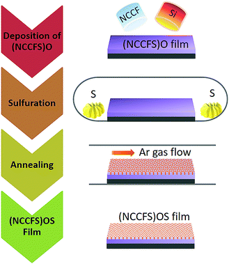 | ||
| Fig. 1 Schematic diagram of the (NCCFS)O film preparation and sulfuration process (NiCrCuFe referred to as NCCF). | ||
X-ray diffraction (XRD) patterns with Cu-Kα radiation are obtained at room temperature. The composition and homogeneity of the films are evaluated by Rutherford backscattering spectroscopy (RBS). The RBS measurements (CEMHTI-CNRS-Orleans, France) are carried out using a 2 MeV alpha particle beam and a current of 15 nA at an incidence normal to the surface of the films. The backscattered particles are collected using silicon detectors at a scattering angle of 165°. The microstructure and thickness of the films are confirmed using a scanning electron microscope (SEM). The reflectance (R) and transmittance (T) spectra are measured using a UV/VIS/NIR spectrophotometer.
3. Results and discussion
3.1. Comparisons of the film structure, composition, and microstructure before and after sulfuration
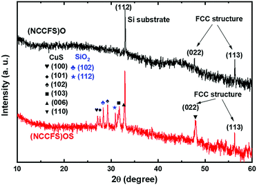
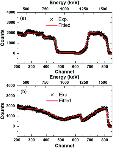
Fig. 2 shows the XRD patterns of the (NCCFS)O films before and after sulfuration. For the as-deposited (NCCFS)O film (black line), three peaks appear at the positions of 2θ = 33.0°, 47.7°, and 56.3°, respectively. The peak at 2θ = 33.0° corresponds to the (112) peak of the Si substrate. The two other peaks correspond to the (022) and (113) peaks of the as-deposited film, indicating the face-centered cubic (FCC) structure. For the (NCCFS)OS film, the XRD pattern (red line) is different from that of the as-deposited film. Eight new peaks are observed at the positions of 2θ = 27.1°, 27.6°, 28.3°, 29.3°, 30.9°, 31.7°, 32.8°, and 47.9°, respectively. The peaks at the positions of 2θ = 27.1°, 27.6°, 29.3°, 31.7°, 32.8°, and 47.9° are indexed to the (100), (101), (102), (103), (006), and (110) peaks, respectively, indicating a hexagonal structure, which may have a similar structure to CuS (powder diffraction file (PDF): #98-002-1479). The other two peaks at the positions of 2θ = 28.3° and 30.9° are indexed to the (102) and (112) peaks, indicating a cubic structure, which may accord with SiO2 (PDF: #98-005-0838). The formation of new compounds after the sulfuration process shows that the crystal structure of the sulfurated film is not only composed of an FCC phase but a mixture of different structures.To have access to the composition of the films, the coatings deposited on the Si substrate are characterized using Rutherford Backscattering Spectroscopy (RBS)38,39 (as shown in Fig. 3). For the as-deposited (NCCFS)O film, as shown in Fig. 3(a), two characteristics are worthy of note. Firstly, the characteristic signals of the backscattering of the alpha particles from the O, Si, Cr, Fe, Ni, and Cu atoms correspond to the remarkable shoulders at the channels of 373, 587, 700, 761, 779, and 812, respectively. Secondly, all the characteristic signals have a good symmetry indicating the fairly uniform distribution of atoms in the (NCCFS)O film. A fitting result, which is represented by a solid red line in Fig. 3(a), shows a good agreement with the experimental data (black cross) and provides a quantitative estimation for the elemental concentration of the (NCCFS)O film. The concentrations of the Ni, Cr, Cu, Fe, Si, and O atoms are shown in Table 1.
For the sulfurated (NCCFS)O film, its RBS result is different from that of the as-deposited one. As shown in Fig. 3(b), first of all, the characteristic signal at the channel of 630 indicates the appearance of the S element.
Moreover, the asymmetric signal peaks of the original metal strongly suggest that the distribution of elements along the depth of the film is no longer uniform but is gradient. As shown in Table 1, all the elements Ni, Cr, Cu, Fe, Si, and O diffuse from the bottom to the top of the film, while S diffuses in the opposite direction in the sulfuration process. It is worth noting that the content of other metal elements at the top of the film is very small compared with those of Cu, O, and Si, which indicates that S may be easier to react with Cu, O, and Si during the sulfuration process.
By calculating the Gibbs free energy change (ΔrGm) of four reactions: FeS + CuO → CuS + FeO, NiS + CuO → CuS + NiO, SiS2 + 2CuO → 2CuS + SiO2, and Cr2S3 + 3CuO → 3CuS + Cr2O3, respectively, as shown in Table 2,40,41 we find that all the ΔrGm values of four reactions are negative, which means that CuS is stable and easier to be formed during the sulfuration process. It accords well with the XRD and RBS results above. The high Ni, Cr, Fe, and Si at. % of the bottom sulfurated film may be due to the uphill diffusion caused by Cu reacting with S.
| Chemical equation | FeS | + | CuO | → | CuS | + | FeO | Total |
| Δ f H m (kJ mol−1) | −81.06 | −141.48 | −35.18 | −253.28 | −65.92 | |||
| Δ f S m (J (mol−1 K−1)) | 101.48 | 76.98 | 105.44 | 101.41 | 28.39 | |||
| Δ r G m (kJ mol−1) | — | — | — | — | −85.03 | |||
| Chemical equation | NiS | + | CuO | → | CuS | + | NiO | Total |
| Δ f H m (kJ mol−1) | −64.34 | −141.48 | −35.18 | −223.98 | −53.34 | |||
| Δ f S m (J (mol−1 K−1)) | 91.37 | 76.98 | 105.44 | 74.10 | 11.19 | |||
| Δ r G m (kJ mol−1) | — | — | — | — | −60.87 | |||
| Chemical equation | SiS2 | + | 2CuO | → | 2CuS | + | SiO2 | Total |
| Δ f H m (kJ mol−1) | −184.18 | −141.48 | −35.18 | −893.96 | −497.18 | |||
| Δ f S m (J (mol−1 K−1)) | 143.67 | 76.98 | 105.44 | 77.76 | −8.99 | |||
| Δ r G m (kJ mol−1) | — | — | — | — | −491.13 | |||
| Chemical equation | Cr2S3 | + | 3CuO | → | 3CuS | + | Cr2O3 | Total |
| Δ f H m (kJ mol−1) | −304 | −141.48 | −35.18 | −1095.49 | −472.59 | |||
| Δ f S m (J (mol−1 K−1)) | 281.41 | 76.98 | 105.44 | 177.9 | −18.13 | |||
| Δ r G m (kJ mol−1) | — | — | — | — | −460.39 | |||
Fig. 4 shows the surface and cross-section SEM images of the as-deposited (NCCFS)O film. The as-deposited film has a smooth surface as shown in Fig. 4(a) and a clear interface between the film and substrate with a film thickness of 466 nm is observed as shown in Fig. 4(b).
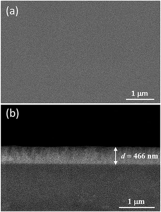 | ||
| Fig. 4 Microstructure of the as-deposited (NCCFS)O film. (a) Surface SEM image. (b) Cross-section SEM image. | ||
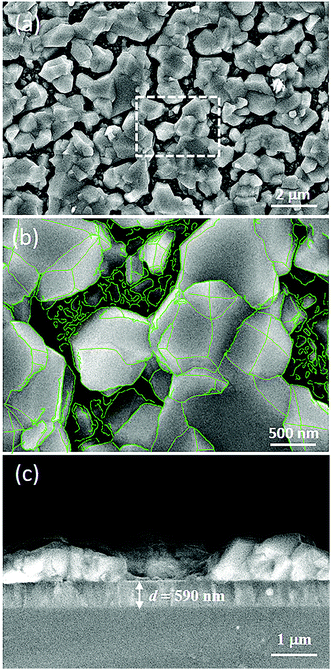
Fig. 5 shows the surface and cross-section SEM images of the sulfurated (NCCFS)O film. As shown in Fig. 5(a), the smooth surface before the sulfurated process transforms into an island-like structure with a plethora of polyhedrons with sharp edges and corners after the sulfuration process. Fig. 5(b) shows a partially enlarged view of the dashed-line-marked area in Fig. 5(a). The edges of the polyhedrons are highlighted with green lines. According to the cross-section SEM image as shown in Fig. 5(c), the island-like structure of the sulfurated (NCCFS)O film is a huge 3-dimensional structure, and the clear interface between the island-like structure and substrate with a film thickness of about 590 nm is observed. The thickness change may be caused by the interface moving due to the Kirkendall effect while island-like structures of the sulfurated (NCCFS)O film may be similar to the 3-dimensional nanostructures formed by the Kirkendall effect through metal thermal oxidation.42,43 The (NCCFS)OS film has not been broken and there is only a slight change in thickness, indicating stability during the sulfuration process.
3.2. Enhancement of the visible-near-infrared absorption for the (NCCFS)OS film
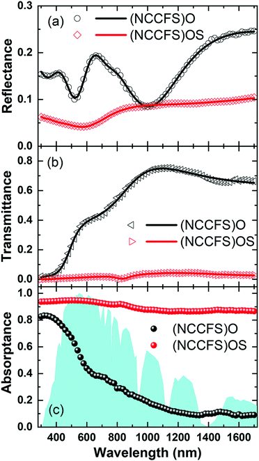
From Fig. 6, the average reflectance (![[R with combining macron]](https://www.rsc.org/images/entities/i_char_0052_0304.gif) ) of the (NCCFS)O film is 0.16, while the (NCCFS)OS film has a lower reflectance and shows relatively smaller change. The average transmittance (
) of the (NCCFS)O film is 0.16, while the (NCCFS)OS film has a lower reflectance and shows relatively smaller change. The average transmittance (![[T with combining macron]](https://www.rsc.org/images/entities/i_char_0054_0304.gif) ) of the (NCCFS)O film is 0.54 in the wavelength range of 300–1700 nm, in contrast, the transmittance of the (NCCFS)OS film is near zero. As a result, the average absorptance (Ā) of the (NCCFS)OS film reaches up to 0.90 compared with the (NCCFS)O film (Ā = 0.30).
) of the (NCCFS)O film is 0.54 in the wavelength range of 300–1700 nm, in contrast, the transmittance of the (NCCFS)OS film is near zero. As a result, the average absorptance (Ā) of the (NCCFS)OS film reaches up to 0.90 compared with the (NCCFS)O film (Ā = 0.30).
While the film is thick, the reflectance of the film can be calculated using the following equation as follows:44
 | (1) |
 | (2) |
From eqn (1) and (2), a high value of k will increase the reflectance while a low k will decrease the absorptance. Only when the value of k is moderate could a high absorptance be caused. When the value of n2 > k2 + 1, R increases monotonically with n, in contrast, when n2 < k2 + 1, R decreases monotonically with n. To find the reason for the higher absorptance of the (NCCFS)OS film, we fit the effective optical constants n and k of the (NCCFS)O and (NCCFS)OS films.
Fig. 7 shows the fitted effective optical constants of the (NCCFS)O and (NCCFS)OS films. For the (NCCFS)O and (NCCFS)OS films, both the values of k are less than 1 and most values of n are more than 1.4, in other words, n2 > k2 + 1. In this case, the low refractive index results in low reflectance, and the high extinction coefficient results in high absorptance. As shown in Fig. 7, the lower refractive index and higher extinction coefficient of the (NCCFS)OS film, compared to that of the (NCCFS)O film, will cause lower reflectance and higher absorptance.
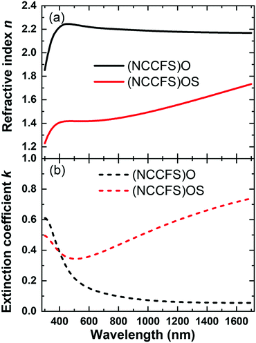 | ||
| Fig. 7 Fitted effective optical constants of the (NCCFS)O films before and after sulfuration. (a) Refractive index (n) and (b) extinction coefficient (k). | ||
The changes of the effective optical constants (the decrease of n and increase of k) of the (NCCFS)OS film may originate from the low refractive index (0.6–1.7 at 300–1700 nm) and high extinction coefficient (0.2–2.5 at 300–1700 nm) of CuS.45 Based on the points of view discussed above, these changes of the effective optical constants could significantly increase the absorptance of the (NCCFS)OS film. In other words, the high absorptance of the (NCCFS)OS film may be caused by the formation of the CuS phase in the sulfuration process.
To figure out the effect of CuS on absorptance, we calculate the reflectance and absorptance of the CuS film in the range of 300–1700 nm (see the ESI for detailed calculations). The average reflectance of the CuS film is 0.35 and the average optical absorptance is only 0.63 in the range of 300–1700 nm. This result strongly indicates that CuS is just one of the reasons for high absorptance and there are some other reasons also for the increase in the absorptance.
The RBS result of the (NCCFS)OS film (Fig. 3) indicates a gradient distribution of elements along with the film thickness after the sulfuration process. As a result, the gradient distribution of elements will make a gradient distribution of the optical constants, which can cause a high absorptance.4,46 Hence, the gradient distribution of elements may be another reason for the increased absorptance.
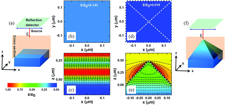
Looking for the effect of the island structure on absorptance performance, we carry out theoretical modeling on the surface structures of the (NCCFS)O films before and after sulfuration. The surface structure of the (NCCFS)O film is assumed as a planar model (as shown in Fig. 8(a)) and the island-like structure of the (NCCFS)OS film is simplified as a pyramidal structure with a bottom side length of 0.25 μm and a height of 0.5 μm (as shown in Fig. 8(f)). During the simulation, the planar light source (λ = 600 nm) is placed on the top of the planar and pyramidal structures, and a reflection detector is applied for reflection collection (as shown in Fig. 8(a)). The simulated results are shown in Fig. 8(b–e). From Fig. 8(b)–(d), the normalized reflected electric field (E/E0 = 0.018) of the pyramidal structure is lower than that of the planar structure (E/E0 = 0.145), thereby greatly increasing the absorptance. The cross-section views of the contour map of electric field are shown in Fig. 8(c) and (e) to make this difference stand out.
According to our previous study,47 when the metasurface is designed as the pyramidal structure, there will be a significant improvement of the absorptance in the range of 300–1700 nm due to the excellent impedance match between the structure surface and air. In this work, newly formed CuS, gradient distribution of elements, and the formation of the island-like structures jointly contribute to the increased absorptance in the range of 300–800 nm, while the formation of the island-like structures plays a dominant role in the range of 800–1700 nm.
4. Conclusions
In this study, we report a simple method, sulfuration, to achieve a high absorptance of the film. After the sulfuration process, CuS and SiO2 are formed in the (NCCFS)O film, the surface of the (NCCFS)O film will form an island-like structure, and the distribution of elements along the depth of the film is no longer uniform but gradient. The average optical absorptance of the high-entropy film can achieve 0.9 in the wavelength range of 300–1700 nm after a simple sulfuration process. The increased absorptance of the (NCCFS)OS film may be due to three aspects: newly formed CuS, gradient distribution of elements, and the island-like structures. CuS decreases the n and increases the k of the (NCCFS)OS film, gradient distribution of elements also makes the distribution of optical constants gradient, which causes a high absorptance, and island-like structure can also increase the absorptance. All of them contribute to the high optical absorptance of the (NCCFS)OS film.Conflicts of interest
There are no conflicts to declare.Acknowledgements
The authors would like to acknowledge the financial support from the National Natural Science Foundation of China (NSFC) (Grants No. 51732001, No. U1832219, and No. 51972013), the Beijing Natural Science Foundation (No. 2182035), and the Fundamental Research Funds for the Central Universities.Notes and references
- S. Chu and A. Majumdar, Nature, 2012, 488, 294–303 CrossRef CAS PubMed.
- R. Schmalensee and V. Bulovic, The future of solar energy: an interdisciplinary MIT study, Energy Initiative, Massachusetts Institute of Technology, 2015 Search PubMed.
- N. S. Lewis, Science, 2016, 351, aad1920 CrossRef PubMed.
- C. E. Kennedy, Review of mid- to high- temperature solar selective absorber materials, National Renewable Energy Lab, Golden, CO.(US), 2002 Search PubMed.
- F. Cao, K. McEnaney, G. Chen and Z. Ren, Energy Environ. Sci., 2014, 7, 1615–1627 RSC.
- S. Günes, H. Neugebauer and N. S. Sariciftci, Chem. Rev., 2007, 107, 1324–1338 CrossRef PubMed.
- F. C. Krebs, Sol. Energy Mater. Sol. Cells, 2009, 93, 394–412 CrossRef CAS.
- H. A. Atwater and A. Polman, Nat. Mater., 2010, 9, 205–213 CrossRef CAS PubMed.
- M. Ni, M. K. H. Leung, D. Y. C. Leung and K. Sumathy, Renewable Sustainable Energy Rev., 2007, 11, 401–425 CrossRef CAS.
- S. Linic, P. Christopher and D. B. Ingram, Nat. Mater., 2011, 10, 911–921 CrossRef CAS PubMed.
- C. K. Prier, D. A. Rankic and D. W. C. Macmillan, Chem. Rev., 2013, 113, 5322–5363 CrossRef CAS PubMed.
- Q. C. Zhang, K. Zhao, B. C. Zhang, L. F. Wang, Z. L. Shen, Z. J. Zhou, D. Q. Lu, D. L. Xie and B. F. Li, Sol. Energy, 1998, 64, 109–114 CrossRef.
- Y. Liu, C. Wang and Y. Xue, Sol. Energy Mater. Sol. Cells, 2012, 96, 131–136 CrossRef CAS.
- Y. Wu, C. Wang, Y. Sun, Y. Xue, Y. Ning, W. Wang, S. Zhao, E. Tomasella and A. Bousquet, Sol. Energy Mater. Sol. Cells, 2015, 134, 373–380 CrossRef CAS.
- C. Wang, X. K. Du and T. M. Wang, Adv. Mater. Res., 2007, 26–28, 899–904 CAS.
- N. Selvakumar, N. T. Manikandanath, A. Biswas and H. C. Barshilia, Sol. Energy Mater. Sol. Cells, 2012, 102, 86–92 CrossRef CAS.
- L. Rebouta, A. Sousa, P. Capela, M. Andritschky, P. Santilli, A. Matilainen, K. Pischow, N. P. Barradas and E. Alves, Sol. Energy Mater. Sol. Cells, 2015, 137, 93–100 CrossRef CAS.
- J. P. Meng, X. P. Liu, Z. Q. Fu and K. Zhang, Sol. Energy, 2017, 146, 430–435 CrossRef CAS.
- F. Cao, D. Kraemer, T. Sun, Y. Lan, G. Chen and Z. Ren, Adv. Energy Mater., 2015, 5, 1401042 CrossRef.
- F. Cao, D. Kraemer, L. Tang, Y. Li, A. P. Litvinchuk, J. Bao, G. Chen and Z. Ren, Energy Environ. Sci., 2015, 8, 3040–3048 RSC.
- H. C. Barshilia, N. Selvakumar, K. S. Rajam and A. Biswas, Sol. Energy Mater. Sol. Cells, 2008, 92, 495–504 CrossRef CAS.
- P. Song, Y. Wu, L. Wang, Y. Sun, Y. Ning, Y. Zhang, B. Dai, E. Tomasella, A. Bousquet and C. Wang, Sol. Energy Mater. Sol. Cells, 2017, 171, 253–257 CrossRef CAS.
- Y. Ning, W. Wang, L. Wang, Y. Sun, P. Song, H. Man, Y. Zhang, B. Dai, J. Zhang, C. Wang, Y. Zhang, S. Zhao, E. Tomasella, A. Bousquet and J. Cellier, Sol. Energy Mater. Sol. Cells, 2017, 167, 178–183 CrossRef CAS.
- Y. Ning, W. Wang, Y. Sun, Y. Wu, Y. Liu, H. Man, M. I. Malik, C. Wang, S. Zhao and E. Tomasella, Vacuum, 2016, 128, 73–79 CrossRef CAS.
- X. Du, C. Wang, T. Wang, L. Zhou, B. Chen and N. Ru, Thin Solid Films, 2008, 516, 3971–3977 CrossRef CAS.
- E. Rephaeli and S. Fan, Appl. Phys. Lett., 2008, 92, 211107 CrossRef.
- V. Rinnerbauer, Y. Shen, J. D. Joannopoulos, M. Soljačić, F. Schäffler and I. Celanovic, Opt. Express, 2014, 22(Suppl 7), A1895–A1906 CrossRef CAS PubMed.
- C. Argyropoulos, K. Q. Le, N. Mattiucci, G. D’Aguanno and A. Alù, Phys. Rev. B: Condens. Matter Mater. Phys., 2013, 87, 205112 CrossRef.
- C. Wan, Y. Ho, S. Nunez-Sanchez, L. Chen, M. Lopez-Garcia, J. Pugh, B. Zhu, P. Selvaraj, T. Mallick, S. Senthilarasu and M. J. Cryan, Nano Energy, 2016, 26, 392–397 CrossRef CAS.
- G. Liu, Y. Nie, G. Fu, X. Liu, Y. Liu, L. Tang and Z. Liu, Nanotechnology, 2017, 28, 165202 CrossRef PubMed.
- M. H. Heidari and S. H. Sedighy, J. Opt. Soc. Am. A, 2018, 35, 522–525 CrossRef CAS PubMed.
- Z. Liu, G. Liu, Z. Huang, X. Liu and G. Fu, Sol. Energy Mater. Sol. Cells, 2018, 179, 346–352 CrossRef CAS.
- Y. Zhang, T. T. Zuo, Z. Tang, M. C. Gao, K. A. Dahmen, P. K. Liaw and Z. P. Lu, Prog. Mater. Sci., 2014, 61, 1–93 CrossRef CAS.
- W. Y. Ching, S. San, J. Brechtl, R. Sakidja, M. Zhang and P. K. Liaw, npj Comput. Mater., 2020, 6, 1–10 CrossRef.
- C. Chen, H. Zhang, Y. Z. Fan, W. W. Zhang, R. Wei, T. Wang, T. Zhang and F. S. Li, J. Magn. Magn. Mater., 2020, 502, 166513 CrossRef CAS.
- M. C. Gao, J. W. Yeh, P. K. Liaw and Y. Zhang, High-Entropy Alloys, Springer International Publishing, 2016 Search PubMed.
- W. J. Sheng, X. Yang, J. Zhu, C. Wang and Y. Zhang, Rare Met., 2018, 37, 682–689 CrossRef CAS.
- N. P. Barradas, C. Jeynes and R. P. Webb, Appl. Phys. Lett., 1997, 71, 291–293 CrossRef CAS.
- M. Mayer, SIMNRA, a Simulation Program for the Analysis of NRA, RBS and ERDA, American Institute of Physics Conference Proceedings, 1999.
- J. G. Speight, Lange's handbook of chemistry, McGraw-Hill Education, 2005 Search PubMed.
- K. T. Jacob, D. B. Rao and H. G. Nelson, Oxid. Met., 1979, 13, 25–55 CrossRef CAS.
- D. K. Saa, T. Gries, S. Migot-Choux, J. Ghanbaja, D. Mangin, P. Boulet, S. Laminsi and T. Belmonte, Surf. Coat. Technol., 2016, 295, 13–19 CrossRef.
- A. Altaweel, G. Filipič, T. Gries and T. Belmonte, J. Cryst. Growth, 2014, 407, 17–24 CrossRef CAS.
- M. N. Siddique, A. Ahmed and P. Tripathi, Optik, 2019, 185, 599–608 CrossRef CAS.
- C. J. Diliegros-Godines, D. I. Lombardero-Juarez, R. Machorro-Mejía, R. S. González and M. Pal, Opt. Mater., 2019, 91, 147–154 CrossRef CAS.
- Y. C. Liou and F. H. Lu, Thin Solid Films, 2018, 660, 733–740 CrossRef CAS.
- P. Song, C. Wang, J. Ren, Y. Sun, Y. Zhang, A. Bousquet, T. Sauvage and E. Tomasella, Int. J. Miner., Metall. Mater., 2020, 27, 1371–1378 CrossRef CAS.
Footnotes |
| † Electronic supplementary information (ESI) available: Table S1 and Fig. S1. See DOI: 10.1039/d1ma00507c |
| ‡ Jie Ren and Ping Song contributed equally to this work. |
| This journal is © The Royal Society of Chemistry 2021 |

