
 Open Access Article
 This Open Access Article is licensed under a Creative Commons Attribution-Non Commercial 3.0 Unported Licence
Dual-gated mono–bilayer graphene junctions†
Mingde
Du
 *a,
Luojun
Du
a,
Nan
Wei
b,
Wei
Liu
b,
Xueyin
Bai
a and
Zhipei
Sun
ac
*a,
Luojun
Du
a,
Nan
Wei
b,
Wei
Liu
b,
Xueyin
Bai
a and
Zhipei
Sun
ac
aDepartment of Electronics and Nanoengineering, Aalto University, Espoo FI-02150, Finland. E-mail: mingde.du@aalto.fi
bDepartment of Applied Physics, School of Science, Aalto University, Espoo FI-00076, Finland
cQTF Centre of Excellence, Department of Applied Physics, Aalto University, Espoo FI-00076, Finland
First published on 28th October 2020
Abstract
A lateral junction with an atomically sharp interface is extensively studied in fundamental research and plays a key role in the development of electronics, photonics and optoelectronics. Here, we demonstrate an electrically tunable lateral junction at atomically sharp interfaces between dual-gated mono- and bilayer graphene. The transport properties of the mono–bilayer graphene interface are systematically investigated with Ids–Vds curves and transfer curves, which are measured with bias voltage Vds applied in opposite directions across the asymmetric mono–bilayer interface. Nearly 30% difference between the output Ids–Vds curves of graphene channels measured at opposite Vds directions is observed. Furthermore, the measured transfer curves confirm that the conductance difference of graphene channels greatly depends on the doping level, which is determined by dual-gating. The Vds direction dependent conductance difference indicates the existence of a gate tunable junction in the mono–bilayer graphene channel, due to different band structures of monolayer graphene with zero bandgap and bilayer graphene with a bandgap opened by dual-gating. Simulation of the Ids–Vds curves based on a new numerical model validates the gate tunable junction at the mono–bilayer graphene interface from another point of view. The dual-gated mono–bilayer graphene junction and new protocol for Ids–Vds curve simulation pave a possible way for functional applications of graphene in next-generation electronics.
Introduction
Two dimensional (2D) materials, such as graphene,1 transition metal dichalcogenides (TMDCs)2 and black phosphorus (BP),3 have been extensively investigated due to their unique physical properties. Until now, plenty of remarkable electronic and optoelectronic properties have been demonstrated in 2D materials,4–6 such as ultrahigh carrier mobility of 200![[thin space (1/6-em)]](https://www.rsc.org/images/entities/char_2009.gif) 000 cm2 V−1 s−1 and reduced noise levels in suspended graphene,7,8 high current on/off ratio of 1 × 10⁸ in monolayer MoS2 transistors2 and ambipolar transport in BP transistors,9 as well as an anisotropic photoresponse and chiral light emission in BP and WS2 based devices.10,11 Of particular importance, the electronic structures and physical properties of 2D materials strongly depend on the number of layers, and functional devices can be built based on this principle.12–15 For example, mono- and bilayer graphene possess massless Dirac-like energy band and nearly parabolic dispersion, respectively.6 The strongly distinct band structures of mono- and bilayer graphene make it possible to construct a lateral junction with atomically sharp interface.16–20 Furthermore, bilayer graphene under dual-gate modulation acquires an opened bandgap as large as 200 meV.21,22 Consequently, ambipolar transport and current on/off ratio larger than 104 are obtained in dual-gated bilayer graphene.23,24
000 cm2 V−1 s−1 and reduced noise levels in suspended graphene,7,8 high current on/off ratio of 1 × 10⁸ in monolayer MoS2 transistors2 and ambipolar transport in BP transistors,9 as well as an anisotropic photoresponse and chiral light emission in BP and WS2 based devices.10,11 Of particular importance, the electronic structures and physical properties of 2D materials strongly depend on the number of layers, and functional devices can be built based on this principle.12–15 For example, mono- and bilayer graphene possess massless Dirac-like energy band and nearly parabolic dispersion, respectively.6 The strongly distinct band structures of mono- and bilayer graphene make it possible to construct a lateral junction with atomically sharp interface.16–20 Furthermore, bilayer graphene under dual-gate modulation acquires an opened bandgap as large as 200 meV.21,22 Consequently, ambipolar transport and current on/off ratio larger than 104 are obtained in dual-gated bilayer graphene.23,24
Here, we investigate the interface between dual-gated mono- and bilayer graphene, with two types of top gate electrodes deposited above the graphene channels, covering only bilayer graphene (local top gate, LTG, Fig. 1a) or the whole graphene channel (global top gate, GTG, Fig. 1b). Transfer curves and Ids–Vds curves of the graphene devices are systematically measured with bias voltage Vds applied in opposite directions along the length of the channel. In addition, Ids–Vds curves of the devices are simulated based on a new numerical model with measured transfer curves as the only input. The results of both measurements and numerical simulation indicate that an electronic junction is successfully built at the mono–bilayer graphene interface, and this junction is considerably enhanced when the doping level of graphene is close to zero. The gate tunable mono–bilayer graphene junction is a promising candidate for the practical applications of graphene.
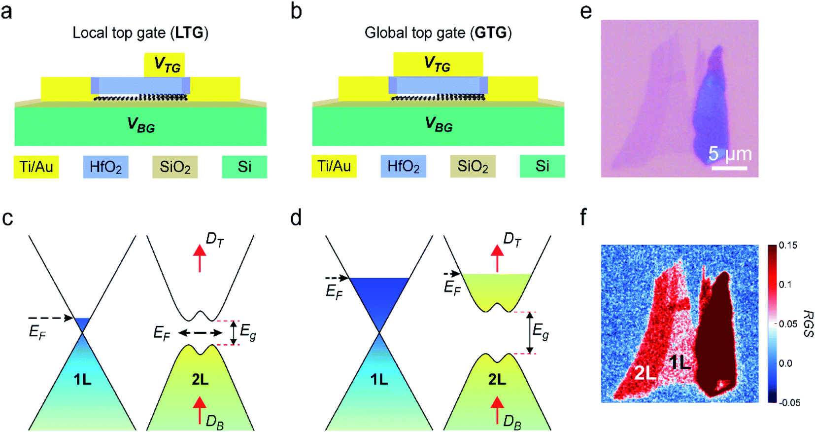 | ||
| Fig. 1 Structure of mono–bilayer graphene junctions. (a and b) Architectures of dual-gated mono–bilayer graphene junction devices with local (a) and global (b) top gate electrodes. (c) Alignment between the Fermi level EF of monolayer (1L) and bilayer (2L) graphene when the doping level is close to zero. (d) Alignment between EF of mono- and bilayer graphene under heavy doping. A bandgap Eg is opened in bilayer graphene in the presence of top and bottom electrical displacement field DT and DB. (e) Optical microscope image of a typical mono–bilayer graphene flake. (f) RGS mapping of the flake in (e). The two areas with RGS of ∼0.06 and ∼0.12 are mono- and bilayer graphene, respectively. | ||
Results and discussion
Architectures of the two different mono–bilayer graphene devices are demonstrated in Fig. 1a and b. The heavily doped silicon substrate works as the back gate electrode, where back gate voltage VBG is applied to modulate both mono- and bilayer graphene in the channels. Top gate electrodes with two different coverings are assigned to the devices, to modulate the graphene channels with top gate voltage VTG. The top gate electrode locally modulates bilayer graphene in the LTG device, while it globally modulates the entire graphene channel of the GTG device. In the presence of VBG and VTG, the induced bottom and top electrical displacement field DB and DT play a double role. Their difference DB − DT determines net doping of mono- and bilayer graphene, and (DB + DT)/2 gives rise to bandgap opening in bilayer graphene.21,23 Therefore, a heterojunction is expected to be built between gapless monolayer graphene and bilayer graphene with an opened bandgap.Conductance of the dual-gated mono–bilayer graphene is expected to highly depend on the Fermi level, as well as the opened bandgap in bilayer graphene. Here, we define a new parameter “effective gate voltage” (VBG-eff and VTG-eff correspond to back and top gate, respectively), that means, the voltage drop between gate electrodes and a point in the graphene channels. For example, when bias voltage Vds is applied on the drain electrode and the source electrode is grounded, the “effective top gate” VTG-eff in the channel ranges from VTG − Vds at the drain to VTG − 0 at the source. VTG-eff can be approximated uniform in the graphene channel when Vds is remarkably smaller than VTG, whereas it significantly changes along the length of the channel when Vds is comparable with VTG. As illustrated in Fig. S1,† when Vds is applied on the electrode connected to monolayer graphene and the electrode connected to bilayer graphene is grounded, VTG-eff in the monolayer section is lower than that in the bilayer section, and this configuration is called the “Mb” mode. Otherwise, in the opposite case when the Vds is applied on the electrode connected to bilayer graphene, VTG-eff in the monolayer section is higher than that in the bilayer section, and this configuration is called the “Bm” mode. Since VTG-eff directly influences the doping level and further the conductance of graphene, the difference between VTG-eff in Mb and Bm modes results in different conductance of the graphene channel. Meanwhile, the change of VTG-eff results in different bandgap opened in bilayer graphene, which contributes to the conductance change of the graphene channel as well. As illustrated in Fig. 1c, when the net doping of graphene determined by DB − DT is close to zero, the channel conductance can be readily tuned by a small shift of gate voltage. However, when the net doping of graphene is quite heavy (Fig. 1d), the channel conductance tends to saturate and is almost independent of gate voltage. Therefore, the Ids–Vds curves measured with Vds in opposite directions are expected to considerably differ from each other when the gate voltages approach the charge neutrality point (CNP).
In order to validate the principle design, mono–bilayer graphene flakes are carefully selected after mechanical exfoliation, followed by device fabrication. The optical microscope image of a typical graphene flake is shown in Fig. 1e, and its thickness is characterized by two methods. Based on the Raman spectrum shown in Fig. S2,† mono- and bilayer graphene areas in this flake can be identified according to the ratio of 2D/G and Lorentzian fitting of 2D peaks.25 Additionally, the thickness of graphene could be confirmed by means of the relative green shift (RGS) based on optical microscope images.26–28Fig. 1f demonstrates RGS results of this typical graphene flake. The two areas with RGS values of ∼0.06 and ∼0.12 are mono- and bilayer graphene. The agreement between the results of Raman and RGS proves the reliability of RGS based graphene thickness identification in our experiments. Details of Raman and RGS based characterization are explained in the Experimental section. In the following sections, the thickness of the two graphene flakes shown in Fig. S3a and b† is characterized using the RGS method. Based on the RGS results in Fig. S3c and d,† both of the two flakes are composed of distinct mono- and bilayer graphene areas. Next, LTG and GTG dual-gated graphene devices are fabricated with the two flakes through a standard microfabrication process as illustrated in Fig. S4† and described in the Experimental section, and optical microscope images of the fabrication process are shown in Fig. S5.†
Transport properties of the graphene junction devices are firstly investigated using Ids–Vds curves measured in Mb and Bm modes. Fig. 2a–c demonstrate Ids–Vds curves of the LTG device measured at various gate voltages, showing that the Ids of Mb measurements is different from that of Bm measurements. The significant difference between Ids of Mb and Bm measurements is a characteristic of the electronic junction in the mono–bilayer graphene channel, because the Ids of uniform channel measured in Mb and Bm modes should be the same. It is apparent that this Ids difference can be greatly modulated by VTG and VBG, similar to the modulation of graphene conductance in transfer curves. In addition, Ids–Vds curves of the GTG device measured at various gate voltages are demonstrated in Fig. 2d–f, where less difference between Ids of Mb and Bm measurements is found. In order to quantitatively compare the Ids–Vds curves of Mb and Bm measurements, the ratio of Ids measured in Mb and Bm modes (Mb/Bm Ids ratio) is calculated, and the results of LTG and GTG devices are shown in Fig. 2g and h, respectively. For both LTG and GTG devices, the Mb/Bm Ids ratio maintains ∼1.0 when Vds < 0.5 V, meaning that the mono–bilayer graphene works just like a uniform material. Nevertheless, this ratio greatly fluctuates around 1.0 when Vds > 1 V, indicating that an effective electronic junction is built at the mono–bilayer graphene interface. The maximum ratio is achieved at decreased VTG (−3 V, −4 V, and −5 V for the LTG device and 2 V, 0 V, and −2 V for the GTG device) when VBG is increased, as indicated by the white arrows in Fig. 2g and h. The Mb/Bm Ids ratio can be as high as roughly 1.3, in other words, the difference between Ids of Mb and Bm measurements is around 30%. The reason behind the gate tunable Mb/Bm Ids ratio could be explained by the transfer curves shown in the following section.
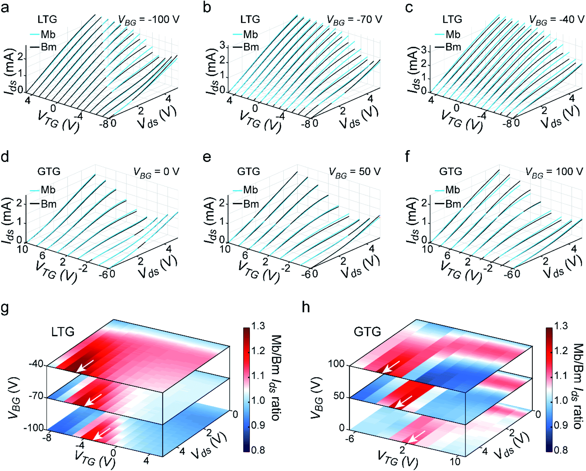 | ||
| Fig. 2 I ds–Vds curves of mono–bilayer graphene junction devices. (a–c) Ids–Vds curves of the LTG device measured at VBG = −100 V, −70 V and −40 V. (d–f) Ids–Vds curves of the GTG device measured at VBG = 0 V, 50 V and 100 V. (g) Mb/Bm Ids ratio calculated with the data of the LTG device in (a–c). (h) Mb/Bm Ids ratio calculated with the data of the GTG device in (d–f). The maximum Mb/Bm Ids ratios, as indicated with white arrows, are obtained at decreased VTG when VBG is increased. | ||
Fig. 3a and b show the transfer curves of LTG and GTG devices measured in the Mb mode. For both LTG and GTG devices, VTG at charge neutrality points (VTG-CNP) is shifted approaching negative when VBG is increased from −100 V to 100 V with 10 V steps, indicating that the doping level of graphene is jointly tuned by both VTG and VBG. As shown in Fig. 3a, channel resistance Rds at charge neutrality points (Rds-CNP) of the LTG device has a minimum value of 3.27 kΩ at VBG = 70 V, whereas the Rds-CNP of the GTG device monotonically decreases from 21.45 kΩ to 9.48 kΩ as VBG is increased. VTG-CNP values in the transfer curves of Fig. 3a and b are extracted and plotted in Fig. 3c, showing that VBG and VTG-CNP have a roughly linear relationship similar to the published results of dual-gated graphene devices.21,29 The transfer curves measured in the Bm mode and corresponding VTG-CNP, as shown in Fig. S6,† exhibit little difference from the results in Fig. 3a–c, because the Vds of 0.1 V in transfer curves measurements leads to little difference between VTG-eff in Mb and Bm modes. VTG values for the maximum Mb/Bm Ids ratio indicated with white arrows in Fig. 2g and h are present as red in Fig. 3c. In particular, VTG-CNP of the GTG device at VBG = 100 V, 50 V and 0 V are almost the same as VTG where maximum Mb/Bm Ids ratios in the GTG device are achieved. The similar VBG dependence of VTG-CNP and VTG at the maximum Mb/Bm Ids ratios suggests that the junction between dual-gated mono- and bilayer graphene heavily depends on the overall doping of graphene determined by DB and DT. As shown in Fig. 3d, for both the LTG and GTG devices, the maximum Mb/Bm Ids ratio is increased when Rds-CNP is decreased. Since the decreased Rds-CNP mainly results from the decreased bandgap of bilayer graphene, it is reasonable to say that the gate tunable bandgap opened in bilayer graphene contributes to the generation of this directional junction as well.
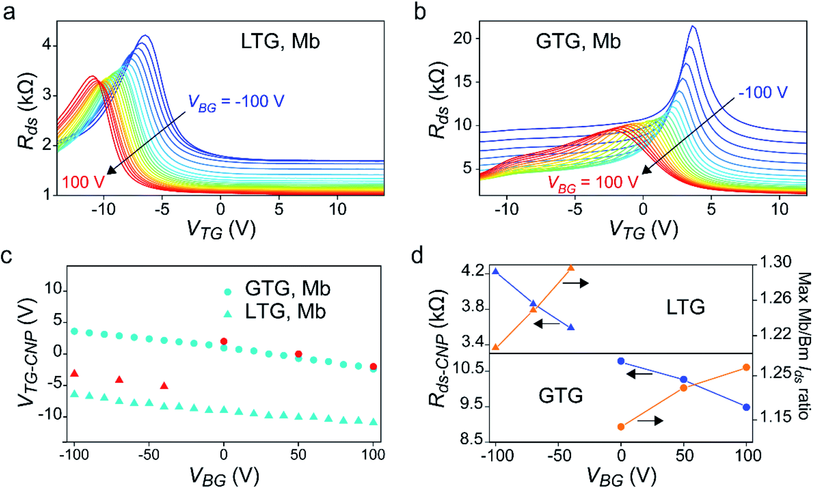 | ||
| Fig. 3 Transfer curves of mono–bilayer graphene junction devices measured in the Mb mode. (a and b) Transfer curves of LTG (a) and GTG (b) graphene junction devices measured at various VBG. The VBG ranges from −100 V to 100 V with 10 V steps in the measurements. (c) VTG at charge neutrality point (VTG-CNP) of the transfer curves in (a) and (b). The red markers indicate where maximum Mb/Bm Ids ratios are obtained, as shown in Fig. 1(g) and (h). (d) Dependence of Rds at charge neutrality point (Rds-CNP) in the transfer curves and maximum Mb/Bm Ids ratios in Ids–Vds curves on gate voltages. | ||
As further proof of the relation between the mono–bilayer graphene junction and gate voltages, a novel numerical model for simulating Ids–Vds curves based on measured transfer curves is proposed. Ids–Vds curves of graphene devices at high electric field when Vds ≫ 0.1 V have been extensively studied based on both experimental measurements and theoretical simulation.30,31 Results of the various models can perfectly explain and quantitatively fit the measured Ids–Vds curves. Nevertheless, there are multiple parameters (such as gate voltages at CNP, capacitance of dielectric layers, drift velocity of carriers, etc.) in these models that need to be measured or estimated initially, increasing a certain degree of difficulty and complexity. For easing the simulation process, a new numerical model is proposed to simulate output Ids–Vds curves with measured transfer curves as the only input, without any additional parameters needed to be measured or estimated. In the new model, every point in the Ids–Vds curves is determined using the formula: Ids = Vds/Rds, where Rds is simulated channel resistance based on the measured transfer curves. Taking the measurement of the LTG device at VBG = −100 V as an example (Fig. 4a), the low bias voltage Vds = 0.1 V in transfer curve measurements has little effect on VTG-eff, therefore VTG-eff is assumed to be equal to VTG at every point in the graphene channel. The measured transfer curve describes a function: Rds = fR(VTG), as illustrated in Fig. 4b. Since the steps of VTG sweeping are quite small (0.28 V for LTG device measurements and 0.24 V for GTG device measurements), the curve between two measured points can be assumed to be linear. As illustrated in Fig. S7,† the corresponding Rds for an arbitrary top gate V0 can be calculated with the formula: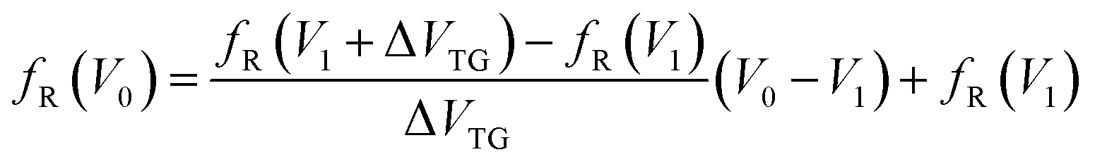 , where V1 is the lower VTG point neighboring V0 in the transfer curve and ΔVTG is the sweeping step of VTG; details of the derivation of this formula are explained in Fig. S7.† When top gate voltage VT0 and source–drain bias voltage Vd0 are applied on the device, the electric potential in graphene channel changes from 0 V at the source (S) electrode to Vd0 at the drain (D) electrode as illustrated in Fig. 4c. Initially, the distribution of electric potential in the channel is assumed to be linear. Namely, if the positions of the source and drain are defined as x = 0 and x = L, the electric potential at position x along the channel length is x/L × Vd0 (Fig. 4c). As a result, VTG-eff at position x in the graphene channel is VT0 − x/L × Vd0. Therefore, VTG-eff at different positions in the graphene channel ranges from VT0 − Vd0 to VT0, and total Rds of the channel can be calculated with the transfer curve in the range of VT0 − Vd0 to VT0 in Fig. 4b. To calculate total Rds, the whole graphene channel is divided into 100 sections with an identical length of L × 1/100 (Fig. 4d). Effective top gate VTG-eff of the n-th section at xn = L × n/100 is VT0 − xn/L × Vd0 = VT0 − n/100 × Vd0, and as a result, resistance of this section is Rn = fR(VT0 − n/100 × Vd0) × 1/100. Finally, resistance of the whole channel is calculated as Rds = ∑Rn = 1/100 × ∑ fR(VT0 − n/100 × Vd0), and the Ids at bias voltage Vd0 in Ids–Vds curve is Id0 = Vd0/Rds. The Ids–Vds curves of the GTG device can be simulated in a similar manner, with its own transfer curves as input.
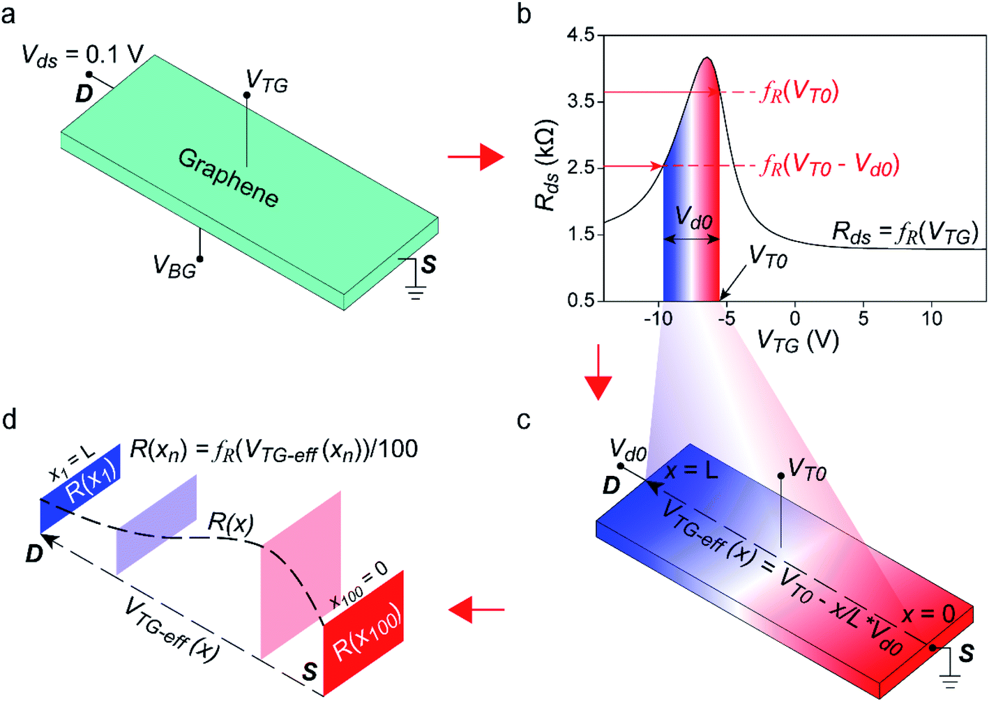 | ||
| Fig. 4 Schematic of the model for simulating Rds. (a) Nearly uniform distribution of electric potential in the graphene channel when Vds = 0.1 V is applied for transfer curves measurements. (b) Rds of graphene channel is assumed to be a function fR of VTG: Rds = fR(VTG), which is described by the transfer curves. Total Rds of the graphene channel measured at top gate voltage VT0 and source–drain bias voltage Vd0 can be calculated based on the curve in the colored range. (c) When top gate voltage VT0 and bias voltage Vd0 are applied on a graphene device, VTG-eff at different positions in the graphene channel are assumed to linearly change from VT0 − Vd0 at drain (D) electrode to VT0 at source (S) electrode. (d) The whole graphene channel is divided into 100 sections along its length, and the resistance R(xn) of a section at xn is defined as 1/100 of fR(VTG-eff(xn)), VTG-eff(xn) is the effective top gate at xn. | ||
To assess the simulation model, simulated Ids–Vds curves of LTG and GTG devices are compared with respect to the measured results. Fig. 5a–d present the simulated (Sim) Ids–Vds curves of LTG and GTG devices at the gate voltages in Fig. 2c and f, as well as the measured (Mea) results demonstrated for straightforward comparison. Apparently, the simulation accuracy seems quite acceptable at most of the (VTG, Vds) combinations, while the difference between simulated and measured Ids–Vds curves is enlarged at specific (VTG, Vds) combinations. This rule can be quantitatively understood with the ratio of simulated and measured Ids (Ids Sim/Mea ratio) shown in Fig. 5e–h, where the white dashed lines are defined by VTG − Vds = VTG-CNP. The Ids Sim/Mea ratio fluctuates between 0.9 and 1.1 at (Vds, VTG) combinations far from the white dashed lines, in other words, the simulation error is less than 10% when the graphene is heavily doped by dual-gating. Therefore, the dual-gated mono–bilayer graphene works like a uniform material as assumed in the simulation model, and this result could be interpreted with the transfer curves in Fig. 2a and b, indicating that Rds tends to be independent of VTG, when VTG is far from CNPs. In contrast, the Ids Sim/Mea ratio at (Vds, VTG) combinations close to the white lines can be lower than 0.4. In other words, the simulation error is larger than 60% when the doping level of dual-gated graphene is close to zero, where Rds values of the devices are substantially sensitive to the shift of VTG according to the curves in Fig. 3a and b. The Ids Sim/Mea ratios of LTG and GTG devices under other conditions shown in Fig. S8† also confirm the dependence of simulation error on VTG − Vds. Since the graphene channel is assumed to be uniform in the simulation model, the considerable simulation error indicates that the graphene channel does not work as a uniform material, in other words, there is a junction built at the dual-gated mono–bilayer graphene interface. Accordingly, it is reasonable to say that the dual-gated mono–bilayer graphene works like a uniform channel at heavy doping, while like a heterojunction when the doping is close to zero. The gate dependent Mb/Bm Ids ratios and Sim/Mea Ids ratios suggest that a gate tunable electronic junction is successfully built in dual-gated mono–bilayer graphene, and the junction tends to be remarkable when the dual-gating induced doping is close to zero.
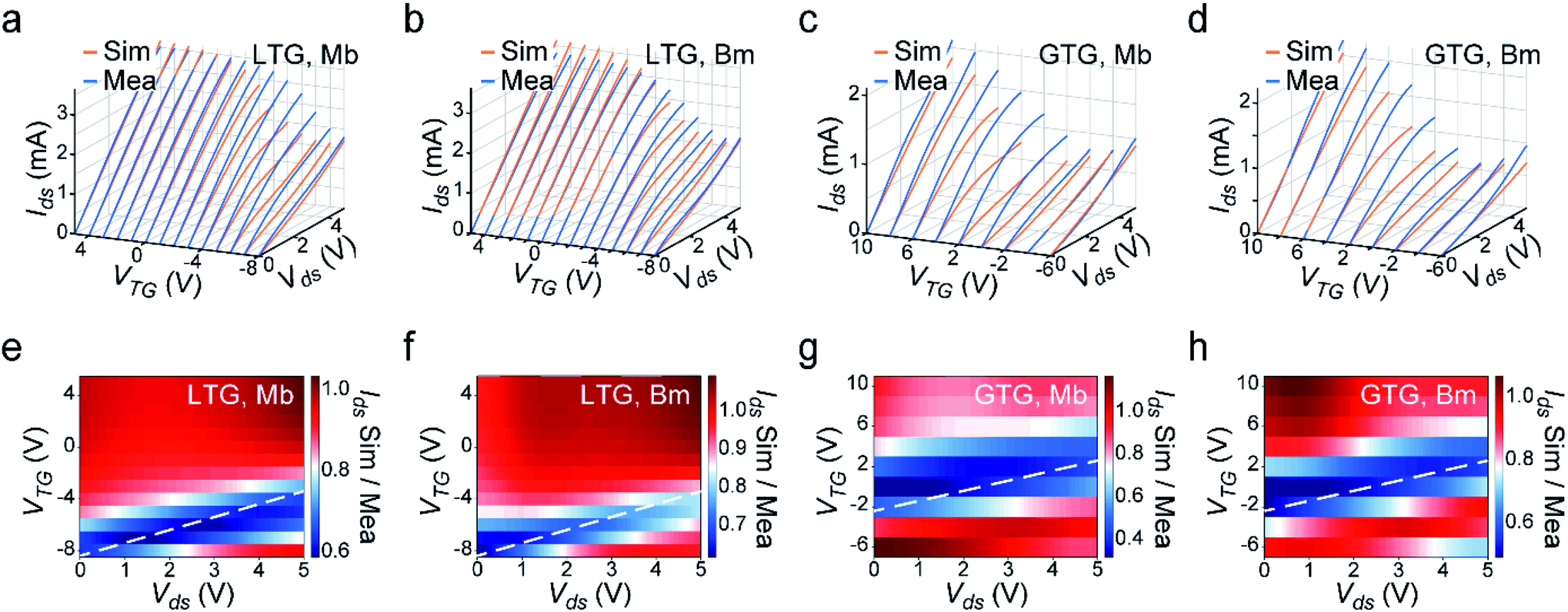 | ||
| Fig. 5 Comparison between simulated and measured Ids–Vds curves. (a–d) Measured (Mea) Ids–Vds curves shown in Fig. 2 and the simulated (Sim) results based on transfer curves in Fig. 3 and S6.†VBG of LTG and GTG devices are −40 V and 100 V. (e–h) Ratio of Ids Sim/Mea calculated with the data in (a–d). The red areas with Sim/Mea ≈ 1 correspond to high accuracy Rds simulation, while the blue areas with Sim/Mea ≪ 1 present low simulation accuracy, because the simulated Ids is much smaller than the measured counterpart. The white dashed lines correspond to VTG − Vds equals to VTG-CNP in Fig. 3 and S6.† | ||
Conclusion
In conclusion, directional electronic transport across a dual-gated mono–bilayer graphene interface is systematically investigated, and a new protocol for Ids–Vds curve simulation is proposed. The measured Ids–Vds curves demonstrate that the mono–bilayer graphene has different conductance under bias voltage Vds in opposite directions (Mb and Bm modes), indicating that an electronic junction is built at the atomically sharp mono–bilayer graphene interface. Additionally, the gate dependent Mb/Bm Ids ratio and Ids–Vds curve simulation indicate that this electronic junction is gate tunable, and the junction could be enhanced when the doping level of graphene is close to zero. Overall, the electrical measurements and numerical simulation prove the existence of a gate tunable junction at the dual-gated mono–bilayer graphene interface. Besides, the proposed simulation model explains Ids–Vds curves at a high electric field in a novel way and simplifies the prediction of output Ids–Vds curves with measured transfer curves. In the future, the mono–bilayer graphene junction can be enhanced by enlarging the bandgap opening of bilayer graphene with novel device structures,23,24 thus the junction would be more functional and valuable. These results indicate that dual-gated mono–bilayer graphene junctions are promising candidates for functional electronics in the future.Experimental section
Preparation and characterization of graphene flakes
Graphene flakes are obtained by scotch tape based mechanical exfoliation of highly oriented pyrolytic graphite (2D semiconductors), and transferred to a cleaned Si wafer with a 280 nm thick SiO2 top layer. The thickness of graphene flakes is critical in this project, so that they are carefully characterized by two methods before device fabrication. The first method is based on the color contrast of the optical microscope (Olympus BX60) images. Green channel G0 in the RGB value of pixels in the optical images is extracted with a custom MATLAB script, and RGS is defined as RGS = (G0 − Gs)/Gs, where Gs is the averaged green value of bare Si/SiO2 areas.26–28 The areas of mono- and bilayer graphene should have RGS values of ∼0.06 and ∼0.12, respectively. The second method is the Raman spectrum. Graphene flakes are characterized using a Raman spectrometer (Horiba LabRAM HR) with a 514 nm excitation laser. According to the ratio of 2D/G and Lorentz fitting of 2D peaks, areas of mono- and bilayer graphene can be identified.25 Consistency between the results of RGS and Raman characterization indicates that RGS characterization based on our equipment is reliable for identifying the graphene thickness.Device fabrication
The graphene devices are fabricated through the process flow illustrated in Fig. S4.† Firstly, source and drain electrodes of 5 nm/100 nm Ti/Au are deposited through standard electron beam lithography (EBL, Vistec EBPG 5000), electron beam evaporation (MASA IM-9912) and lift-off process. Graphene areas between the source and drain electrodes are further patterned to a regular shape with EBL and reactive ion etching (RIE, Oxford Instruments PlasmaLab 80 Plus), to avoid the influence of interface states.16 The residues of EBL resist after RIE is removed with acetone, followed by high vacuum annealing (AML – AWB wafer bonding machine) at 200 °C for 2 hours. Right after annealing, the devices are transferred to evaporation equipment and a 2 nm thick Al layer is deposited on graphene. Subsequently, the Al layer is oxidized on a 130 °C hotplate in air for 3 min to form a Al2O3 seeding layer.29 Above the Al2O3 layer, a 20 nm thick HfO2 layer is grown by atomic layer deposition (ALD, Beneq TFS-500) at 200 °C, with TDMAH and water used as hafnium and oxidant sources. Finally, top gate electrodes are deposited through a process same to that of source and drain electrodes. The fabricated devices are connected to a printed circuit board for electrical measurements by wire bonding (Delvotec 53XX). Optical microscope images of the fabrication process are demonstrated in Fig. S5,† showing that source and drain electrodes are arranged to be parallel with the interface between mono- and bilayer graphene.Electrical measurements
All the electrical measurements in this article are carried out with a semiconductor device parameter analyzer (Agilent B1500A) under ambient conditions. The Ids–Vds curves are measured by sweeping the bias voltage Vds at various combinations of VTG and VBG, and transfer curves are measured by sweeping the top gate voltage at various back gate voltages. All the measurements are conducted at Vds in opposite directions (Mb and Bm modes) along the channel length.Numerical simulation
Values of simulated Rds and Ids are calculated with a custom MATLAB script based on the measured transfer curves.Conflicts of interest
The authors declare no competing financial interest.Acknowledgements
We acknowledge the provision of facilities by Aalto University at the OtaNano – Micronova Nanofabrication Centre and the OtaNano – Low Temperature Laboratory, and the funding from the Academy of Finland (276376, 295777, 312297, and 314810), Academy of Finland Flagship Programme (320167, PREIN), the European Union's Horizon 2020 research and innovation program (820423,S2QUIP), and ERC (834742).References
- K. S. Novoselov, A. K. Geim, S. V. Morozov, D. Jiang, Y. Zhang, S. V. Dubonos, I. V. Grigorieva and A. A. Firsov, Science, 2004, 306, 666–669 CrossRef CAS.
- B. Radisavljevic, A. Radenovic, J. Brivio, V. Giacometti and A. Kis, Nat. Nanotechnol., 2011, 6, 147–150 CrossRef CAS.
- L. Li, Y. Yu, G. J. Ye, Q. Ge, X. Ou, H. Wu, D. Feng, X. H. Chen and Y. Zhang, Nat. Nanotechnol., 2014, 9, 372–377 CrossRef CAS.
- F. Bonaccorso, Z. Sun, T. Hasan and A. C. Ferrari, Nat. Photonics, 2010, 4, 611–622 CrossRef CAS.
- A. H. Castro Neto, F. Guinea, N. M. R. Peres, K. S. Novoselov and A. K. Geim, Rev. Mod. Phys., 2009, 81, 109–162 CrossRef CAS.
- A. C. Ferrari, F. Bonaccorso, V. Fal'ko, K. S. Novoselov, S. Roche, P. Bøggild, S. Borini, F. H. L. Koppens, V. Palermo and N. Pugno, et al. , Nanoscale, 2015, 7, 4598–4810 RSC.
- K. I. Bolotin, K. J. Sikes, Z. Jiang, M. Klima, G. Fudenberg, J. Hone, P. Kim and H. L. Stormer, Solid State Commun., 2008, 146, 351–355 CrossRef CAS.
- Z. Cheng, Q. Li, Z. Li, Q. Zhou and Y. Fang, Nano Lett., 2010, 10, 1864–1868 CrossRef CAS.
- L. Li, Y. Yu, G. J. Ye, Q. Ge, X. Ou, H. Wu, D. Feng, X. H. Chen and Y. Zhang, Nat. Nanotechnol., 2014, 9, 372–377 CrossRef CAS.
- H. Yuan, X. Liu, F. Afshinmanesh, W. Li, G. Xu, J. Sun, B. Lian, A. G. Curto, G. Ye and Y. Hikita, et al. , Nat. Nanotechnol., 2015, 10, 707–713 CrossRef CAS.
- Y. J. Zhang, T. Oka, R. Suzuki, J. T. Ye and Y. Iwasa, Science, 2014, 344, 725–728 CrossRef CAS.
- K. F. Mak, C. Lee, J. Hone, J. Shan and T. F. Heinz, Phys. Rev. Lett., 2010, 105, 136805 CrossRef.
- S. Kim, G. Myeong, W. Shin, H. Lim, B. Kim, T. Jin, S. Chang, K. Watanabe, T. Taniguchi and S. Cho, Nat. Nanotechnol., 2020, 15, 203–206 CrossRef CAS.
- L. Li, J. Kim, C. Jin, G. J. Ye, D. Y. Qiu, F. H. da Jornada, Z. Shi, L. Chen, Z. Zhang and F. Yang, et al. , Nat. Nanotechnol., 2017, 12, 21–25 CrossRef CAS.
- C. Zhang, Y. Chen, J.-K. Huang, X. Wu, L.-J. Li, W. Yao, J. Tersoff and C.-K. Shih, Nat. Commun., 2016, 7, 10349 CrossRef.
- C. P. Puls, N. E. Staley and Y. Liu, Phys. Rev. B: Condens. Matter Mater. Phys., 2009, 79, 235415 CrossRef.
- X. Xu, N. M. Gabor, J. S. Alden, A. M. van der Zande and P. L. McEuen, Nano Lett., 2010, 10, 562–566 CrossRef CAS.
- G. Liu, S. Rumyantsev, M. Shur and A. A. Balandin, Appl. Phys. Lett., 2012, 100, 033103 CrossRef.
- X. Wang, W. Xie, J. Chen and J.-B. Xu, ACS Appl. Mater. Interfaces, 2014, 6, 3–8 CrossRef CAS.
- J. Tian, Y. Jiang, I. Childres, H. Cao, J. Hu and Y. P. Chen, Phys. Rev. B: Condens. Matter Mater. Phys., 2013, 88, 125410 CrossRef.
- Y. Zhang, T.-T. Tang, C. Girit, Z. Hao, M. C. Martin, A. Zettl, M. F. Crommie, Y. R. Shen and F. Wang, Nature, 2009, 459, 820–823 CrossRef CAS.
- K. F. Mak, C. H. Lui, J. Shan and T. F. Heinz, Phys. Rev. Lett., 2009, 102, 256405 CrossRef.
- T. Taychatanapat and P. Jarillo-Herrero, Phys. Rev. Lett., 2010, 105, 166601 CrossRef.
- X. Liu, Z. Wang, K. Watanabe, T. Taniguchi, O. Vafek and J. Li, 2020, preprint, arXiv:2003.11072, https://arxiv.org/abs/2003.11072.
- A. C. Ferrari, J. C. Meyer, V. Scardaci, C. Casiraghi, M. Lazzeri, F. Mauri, S. Piscanec, D. Jiang, K. S. Novoselov and S. Roth, et al. , Phys. Rev. Lett., 2006, 97, 187401 CrossRef CAS.
- J. B. Oostinga, H. B. Heersche, X. Liu, A. F. Morpurgo and L. M. K. Vandersypen, Nat. Mater., 2008, 7, 151–157 CrossRef CAS.
- M. F. Craciun, S. Russo, M. Yamamoto, J. B. Oostinga, A. F. Morpurgo and S. Tarucha, Nat. Nanotechnol., 2009, 4, 383–388 CrossRef CAS.
- S. Russo, M. F. Craciun, M. Yamamoto, S. Tarucha and A. F. Morpurgo, New J. Phys., 2009, 11, 095018 CrossRef.
- S. Kim, J. Nah, I. Jo, D. Shahrjerdi, L. Colombo, Z. Yao, E. Tutuc and S. K. Banerjee, Appl. Phys. Lett., 2009, 94, 062107 CrossRef.
- B. Chakraborty, A. Das and A. K. Sood, Nanotechnology, 2009, 20, 365203 CrossRef.
- I. Meric, M. Y. Han, A. F. Young, B. Ozyilmaz, P. Kim and K. L. Shepard, Nat. Nanotechnol., 2008, 3, 654–659 CrossRef CAS.
Footnote |
| † Electronic supplementary information (ESI) available. See DOI: 10.1039/d0na00547a |
| This journal is © The Royal Society of Chemistry 2021 |