 Open Access Article
Molecular engineering for high-performance fullerene broadband photodetectors†
Mingming
Su
,
Yajing
Hu
,
Ao
Yu
,
Zhiyao
Peng
,
Wangtao
Long
,
Shixin
Gao
,
Ping
Peng
*,
Bin
Su
 and
Fang-Fang
Li
 *
*
State Key Laboratory of Materials Processing and Die & Mould Technology, School of Materials Science and Engineering, Huazhong University of Science and Technology, Wuhan 430074, China. E-mail: ppeng@hust.edu.cn; ffli@hust.edu.cn
First published on 31st December 2020
Abstract
Broadband photodetectors fabricated with organic molecules have the advantages of low cost, high flexibility, easy processing and low-temperature requirement. Fullerene molecules, due to their electron accepting and photoinduced electron transfer properties, are potential materials for photodetectors. However, fullerene has a narrow light absorption spectrum range, and realization of large-area fullerene-based broadband photodetectors remains a challenge. Herein, we broaden the absorption wavelength range of fullerene through molecular engineering, i.e. adding a donor molecule, nickel tetraphenylporphyrin (NiTPP) with strong visible light absorption capacity, onto the fullerene cage to form a donor–acceptor dyad (NiTPP-C60). Moreover, large-area nickel porphyrin–fullerene (NiTPP-C60) single-crystal arrays were prepared by applying a liquid-bridge induced assembly method. Combining the excellent visible light absorption properties of porphyrin and the good electron transport characteristic of fullerene, photodetectors fabricated with NiTPP-C60 single-crystal arrays show a fast photoelectric response with τon < 0.09 s at 350 nm, τon < 0.10 s at 425 nm and τon < 0.08 s at 530 nm, and the highest responsivity of 11.9 A W−1 at 425 nm. This study provides a new strategy toward the fabrication of high-performance fullerene broadband photodetectors and presents a versatile method for the design of large-area well-aligned organic single-crystal arrays for practical electronic applications.
1. Introduction
Photodetectors are devices that convert light signals into electrical signals, which have broad applications in optical interconnection techniques, light-wave communications, circuits, and high-resolution imaging.1–5 According to the working wavelength range, photodetectors are generally classified into narrowband photodetectors and broadband photodetectors. Narrowband photodetectors can accurately detect a specific light through material selection and optical path design. Broadband photodetectors have a wide detection range, and a single device can achieve multi-spectral detection functions. With the increasing application requirements, photodetectors that can only detect a single wavelength no longer satisfied the criteria for multiple detections. Although assembling multiple sets of narrowband detection systems could be applicable, it is costly due to the device packaging and chip integration. Therefore, researchers have paid attention to broadband photodetectors to control the integration cost and simplify the assembly process, and applied them in digital photography, optical sensing, and night vision applications.6–13Traditional broadband photodetectors are prepared from inorganic semiconductor materials (such as Si, MoS2 and InGaAs), whereas, the materials are expensive and the manufacturing process is complicated.14,15 Compared to inorganic semiconductors, organic small-molecule semiconductors have attracted considerable attention in optical detection applications, because of their cost-effectiveness, flexibility, amenability to roll-to-roll large area producing, compatibility with plastic substrates, tunable molecular structures, and broader light range response.13,16–20
Fullerene (C60), as an electron acceptor with fast photoinduced charge transfer properties, is a promising candidate for organic photodetectors. For example, C60 single-crystal arrays and microribbons have been prepared through solvent-assisted methods and exhibited an excellent photoresponse and high photoresponsivity.21,22 However, the weak visible light absorption and high electronic transition energy levels (HOMO → LUMO) of C60 limit its application in broadband photodetectors. To realize a fullerene broadband photodetector, a material with strong absorption in the visible light region was selected to form a heterojunction with fullerene, thereby broadening the absorption spectrum of the device.23–26 For example, Peng and co-workers successfully achieved an excellent broadband optical response from the ultraviolet to the near-infrared region by constructing a fullerene (C60)/AlClPc planar heterojunction structure.23 It showed a high responsivity of 94.4 A W−1, and a detectivity of ∼1.5 × 10¹³ Jones. Gong et al. prepared a bulk heterojunction structure based on a donor–acceptor (D–A) conjugated polymer PBBTPD and tri-PC61BM, which achieved light detection in the wavelength range from 350 nm to 2500 nm, and showed a responsivity of 5 × 10⁻² mA W−1 at 800 nm and detectivity higher than 1011 Jones.27 Lu et al. fabricated a planar heterojunction of CuPc/C60, which exhibited a responsivity of 0.094 A W−1.25 However, the contact area between the donor and acceptor in a planar heterojunction structure is small, which greatly limits the photoelectric conversion efficiency of the device. For bulk heterojunction structures, the transportation of charge carriers to the electrode is sensitive to the morphology and particle size of the material.28 A large particle size will result in a small contact interface area of the donor and acceptor and low efficiency of exciton dissociation, while, if the particle size is too small, the numbers of particles will increase and the transportation of carriers will be restricted.
Thus, we propose to connect an electron donor unit possessing strong absorption in the visible light region to fullerenes to form a single-molecule D–A intramolecular heterojunction. In this way, the excitons generated by light absorption are dissociated inside the molecules, and the generated carriers are also transported within the molecules, which fundamentally avoid the influence of phase separation between the donor and acceptor on the dissociation of excitons.29–35 Porphyrin molecules are macrocyclic conjugated electron-rich compounds that can act as electron donors and exhibit strong absorption in the visible light region.36,37 By contrast, fullerenes are electron-deficient molecules that can act as electron acceptors38 and show strong absorption in the UV region. Modification of a fullerene cage with a porphyrin structure through covalent bonds to form a D–A dyad molecule could realize broad spectral absorption. Moreover, fullerene–porphyrin dyads were found to exhibit photoinduced electron transfer properties,39–42 making them promising candidates for broadband photodetectors.
The photoelectric performance of fullerenes depends heavily on their morphology and crystallinity. Highly ordered crystalline fullerene micro/nano-structures can dramatically enhance the photoresponse performance. One-dimensional (1D) crystalline fullerene structures are of particular interest for optoelectronic devices due to the presence of effective channels for charge transportation, enabling a superior optical and electrical response.43,44 However, the preparation of large-area and highly ordered fullerene micro/nanostructure arrays is challenging and has rarely been reported. One-dimensional fullerene structures obtained from the solution process are generally discontinuous C60 crystals or oriented in one direction at a random position,44–46 which is unfavorable for the fabrication of large-scale integrated devices and impedes their practical applications. Thus, the synthesis of large-area and long-distance ordered fullerene-porphyrin dyad single crystalline arrays is desirable for high-performance broadband photodetectors.
In this work, a fullerene–nickel tetraphenylporphyrin dyad (NiTPP-C60) was synthesized and assembled to a large-area single-crystal microwire array by the “liquid bridge induced assembly” (LBIA) method.47–49 For comparison, crystalline microwire arrays of C60 and NiTTP with different concentrations were prepared as well. The average width of the microwires increases with fullerene concentrations. Attributed to the complementary spectra of C60 and NiTPP in the UV-Vis region, the devices fabricated with NiTPP-C60 microwire arrays as a light-absorbing layer show an excellent broad-spectral response. The performances of the NiTPP-C60 photodetector are superior to those of C60 and NiTPP detectors. The strategy presented here provides a clue for future design and synthesis of functional fullerenes and their large-scale 1D crystal arrays for broadband photodetectors with a spectral response from the ultraviolet to the visible region and even to the near-infrared region.
2. Results and discussion
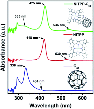
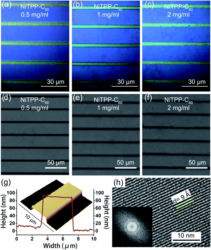
The fullerene–porphyrin dyad (NiTPP-C60) was synthesized according to a previous report.50 UV-vis-NIR spectroscopy is one of the most convenient techniques to study the optical absorption characteristics of materials. Fig. 1 shows the UV-visible absorption spectra of C60, NiTPP, and NiTPP-C60 in dichlorobenzene (o-DCB). C60 exhibits a strong absorption in the ultraviolet region at 336 nm and a weak absorption in the visible region at 404 nm. For NiTPP, a strong absorption peak appears at about 418 nm, which is the Soret absorption band generated by the electron transition of the porphyrin molecule a1μ(π)–eg(π*). Another absorption peak around 530 nm is a Q-band absorption peak generated by an electron transition between the porphyrin molecules a2μ(π)–eg(π*). The absorption spectrum of NiTPP-C60 can be seen as a combination of the absorption spectrum of C60 and NiTPP. NiTPP-C60 exhibits absorptions in the range of 300 to 600 nm, indicating its potential application for broadband photodetectors.To obtain a large-scale photodetector device, a liquid-bridge induced assembly method was applied.51–53 A designed micropillar template (Fig. 2a–c) was used to prepare large-area microwire arrays. The width and height of the microcolumns are 5 μm and 15 μm, respectively, and the spacing between two adjacent microcolumns is 20 μm. Notably, the sidewall of the microcolumn template is modified with heptafluorododecyltrimethoxysilane (FAS) molecules to make its wettability different from the top, which is a key to microwire crystallization. o-Dichlorobenzene (o-DCB) was chosen as the solvent to dissolve NiTPP-C60 for the subsequent crystallization due to its high solubility for fullerene derivatives and slow evaporation rate. Fig. 2d displays the self-assembly process of the microwire arrays. 15 μl of the NiTPP-C60 solution with respective concentrations of 0.5, 1, and 2 mg ml−1 was carefully dropped onto the substrate, followed by gentle covering with a template. The assembled device was then put in an oven for evaporation (80 °C). Single-crystal microwire arrays were successfully crystallized after 12 h. During the preparation process, the fullerene solution is confined in the gaps of the microcolumns, and the top of the lyophilic microcolumn is to adjust the position and size of the microwires, which allow fabrication of large-scale, high-crystallinity and highly ordered microwires.52
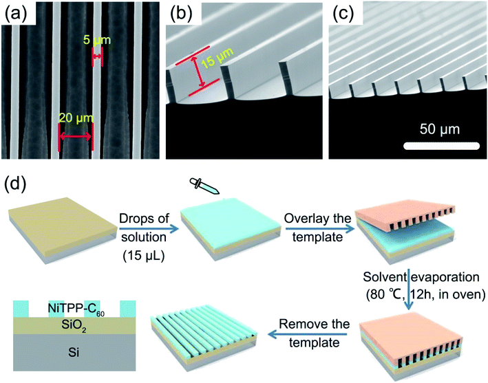 | ||
| Fig. 2 (a–c) SEM images of an asymmetric infiltrating template. (d) Assembly process of one-dimensional microwire arrays of NiTPP-C60. | ||
The optical and scanning electron micrographs of the assembled structures of NiTPP-C60 display a large-area and orderly arranged microwire array (Fig. 3a–f and S1 in the ESI†). The size of the microwires is uniform and no apparent defects or ruptures are present in SEM and optical images. NiTPP-C60 microwires prepared from 1 mg ml−1 solution display smoother surfaces and edges than those from 0.5 mg ml−1 and 2 mg ml−1 NiTPP-C60, which are critical to achieve fast electron transport within the microwire to promote efficient conversion of an optical signal into an electrical signal, thus achieving high device performances. For comparison, the microwire arrays of C60, and NiTPP at the concentrations of 0.5, 1 and 2 mg ml−1 were prepared as well by the same procedures as described for NiTPP-C60 (Fig. S2 and S3†). It is found that the microwire arrays prepared from 1 mg ml−1 solution exhibit better morphology with fewer defects. Notably, the width of microwires is an important parameter for calculating the responsivity of a photodetector, and thus, we prepared five samples at each concentration and randomly selected ten microwires from each sample to count the width. We found that the microwire width is controlled by fullerene concentrations. As the concentration of NiTPP-C60 increases from 0.5 to 2 mg ml−1, the major width distribution increases from 3.15 to 3.5 μm (Fig. S4†). The same tendency was observed for C60 and NiTPP microwires (Fig. S5†). The width statistics of C60, NiTPP and NiTPP-C60 microwires with different concentrations are listed in Table S1.†
The structure of NiTPP-C60 microwires prepared from 1 mg ml−1 solution has better morphology and was further characterized using a three-dimensional (3D) atomic force microscope (AFM) and HRTEM. As shown in Fig. 3g and S6,† the crystal has a flat, clean, and smooth surface with a uniform thickness of ∼90 nm, and the height difference of the microwire in the longitudinal direction is less than 3 nm, which lay the foundation for the high-speed migration of electrons in the microwire.54 AFM tests on C60 and NiTPP microwires prepared from 1 mg ml−1 solution were also performed. Both microwires show smooth, flat surfaces and a uniform height of ∼90 nm, reflecting the high crystallinity of the microwires (Fig. S7†). The HRTEM image of NiTPP-C60 microwires (Fig. 3h) demonstrates the preferred growth orientation of fullerene molecules. It shows clear lattice planes with a measured d value of 9 Å. The fast Fourier transformation (FFT) image (inset image) displays regular single-crystal diffraction spots, implying that the as-formed microwires are highly crystalline.
Photodetection measurements were performed to study the applications of NiTPP-C60 microwire arrays in broadband photodetectors. The device structure fabricated with microwire arrays and the corresponding SEM image are shown in Fig. 4. Gold (Au) as an electrode material was deposited on both ends of the microwires by a thermal evaporation method (Fig. 4a). The effective area between two Au electrodes that directly affects the performance of the device can be determined by the width and the valid numbers of microwires. The numbers of effective microwires can be counted through the SEM image in Fig. 4b.
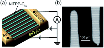 | ||
| Fig. 4 (a) Schematic diagram of the photodetector device based on microwire arrays grown from 1 mg ml−1 NiTPP-C60 and (b) SEM images of the corresponding device. | ||
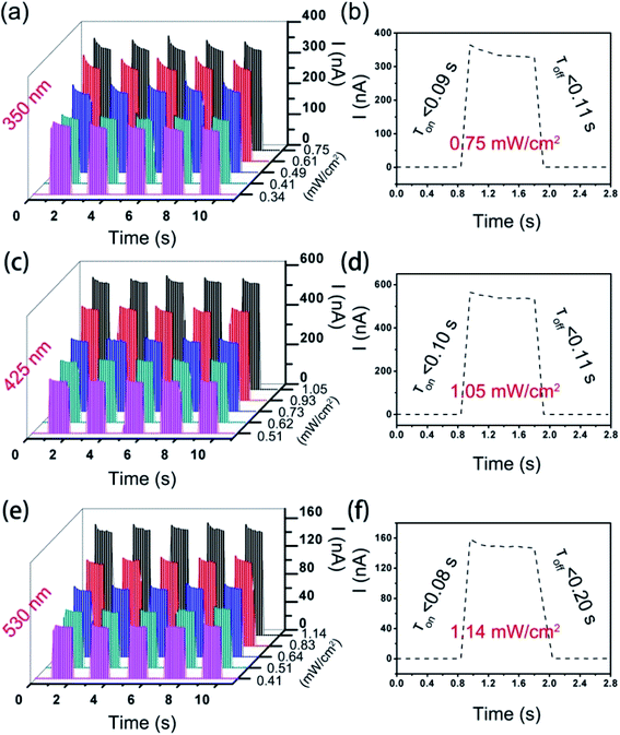
The photocurrent–time (I–T) diagram of the NiTPP-C60 microwire device shows long-term stable photoelectric response characteristics under a periodic light stimulation at 350 nm, 425 nm, and 530 nm, respectively (Fig. 5a, c and e). An increase in optical power density can activate more electron–hole pairs in the microwires and lead to a larger photocurrent. The photocurrent under a 425 nm light source (∼530 nA) is more significant compared with that under 350 nm (∼326 nA) and 530 nm (∼150 nA) light sources, which agrees well with the strongest absorption of NiTPP-C60 at 425 nm. The fast photoresponse of the detector to the three light sources was demonstrated in the single-cycle I–T curves and the response time is 0.08–0.1 s (Fig. 5b: 350 nm, 0.75 mW cm−2; Fig. 5d: 425 nm, 1.05 mW cm−2; Fig. 5f: 530 nm, 1.14 mW cm−2). The photocurrent–voltage (I–V) curves of the devices measured in the dark and under irradiation with three wavelength light sources display a linear relationship between the current and voltage (Fig. S8†), indicating that the microwire arrays are in ohmic contact with the gold electrodes, which is favorable for current input and output.
Correspondingly, the photoelectric detection performances of C60 and NiTPP microwire arrays were also tested. The assembly process and the structures of the devices are the same as those of NiTPP-C60 (Fig. S9a and S10a†). The effective numbers of the microwires between two Au electrodes can be intuitively obtained from SEM images (Fig. S9b and S10b†). As can be seen from the absorption spectrum, C60 only shows strong absorption in the ultraviolet region at ∼340 nm. Therefore, the photoelectric response characteristics of the C60 microwire arrays were measured only at 350 nm UV light on/off (Fig. S9c†). The device showed stable light/dark current during multiple cycle tests, a fast photoresponse of ∼0.09 s and a high photocurrent of ∼270 nA (Fig. S9d†) at an optical power density of 0.75 mW cm−2. NiTPP has two absorption peaks in the visible light region. Therefore, the photoelectric responses of the NiTPP microwires to blue-violet light at 425 nm and green light at 530 nm were explored. The switching performance of the NiTPP microwire-based photodetector is demonstrated in the I–T curve in Fig. S10c–f.† The response is fast, stable and repeatable, showing a response time of ∼0.09 s to the pulsed light at 425 nm and ∼0.15 s at 530 nm. The photocurrents are ∼358 nA at 425 nm under 1.05 mW cm−2 optical power density and ∼100 nA at 530 nm under 1.14 mW cm−2 optical power density. Comparing the results obtained from C60, NiTPP and NiTPP-C60, it was found that molecular engineering by modifying C60 with NiTPP not only broadened the light detection range but also enhanced the intensity of photocurrent.
The performances of photodetectors are reflected primarily by the response time and responsivity. Responsivity (R) is the photocurrent passing through the effective illumination area of a detector at unit optical power, which can be expressed by eqn (1):
 | (1) |
| S = L × W × n | (2) |
| Materials | Light source (nm) | P in [mW cm−2] | τ on (s) | τ off (s) | R [A W−1] |
|---|---|---|---|---|---|
| C60 | 350 | 0.34 | 0.09 | 0.10 | 4.91 |
| NiTPP | 425 | 0.51 | 0.20 | 0.10 | 4.02 |
| 530 | 0.41 | 0.30 | 0.18 | 1.34 | |
| NiTPP-C60 | 350 | 0.34 | 0.09 | 0.14 | 8.92 |
| 425 | 0.51 | 0.09 | 0.10 | 11.9 | |
| 530 | 0.41 | 0.11 | 0.09 | 3.11 |
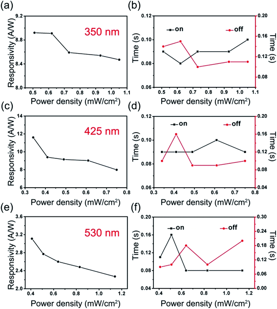
Response time curves of the NiTPP-C60 photodetector under different light sources/power densities are given in Fig. 6b, d and f. A fast photoelectric response was observed during the ascent process (red curve, rise time: 0.08–0.16 s) and the decay process (black curve, decay time: 0.08–0.20 s). The photodetectors based on C60 (Fig. S11†) and NiTPP (Fig. S12†) microwire arrays also exhibit fast light response characteristics. The response time mainly relies on the drift velocity of carriers, which is largely affected by the arrangement of molecules within the crystals. Highly ordered molecular arrangement and the fewer defects in the microwires lead to fast movement of the electrons, thereby accelerating the response times. From the analysis and comparison of two crucial performance parameters of the three photodetectors (Table 1), we can draw the following conclusions: (i) the combination of the excellent light absorption characteristics of porphyrin molecules and the good electron transportation properties of fullerene molecules account for the high photocurrent of NiTPP-C60, (ii) the highly crystalline microwires arrays are responsible for the rapid light response of photodetectors, and (iii) the D–A intramolecular heterojunction facilitates exciton dissociation and charge carrier transportation. The results of fullerene-based broadband photodetectors are compared in Table 2. Our device shows a higher responsivity55–58 and faster response time24,56 than most of the fullerene heterojunction devices.
| Materials | Light source (nm) | P in [mW cm−2] | τ on (s) | τ off (s) | R [A W−1] | Ref. |
|---|---|---|---|---|---|---|
| PDPP3T/PTB7/PC71BM | 680 | — | — | — | 0.25 | 55 |
| 850 | — | — | — | 0.29 | ||
| VTP/PC71BM | 650 | 100 | 0.35 | 0.4 | 0.23 | 56 |
| P3HT/PTB7-Th/PC71BM | 550 | 0.016 | — | — | 0.172 | 57 |
| PCBM/CsPbBr3 | 447 | 3.5 | — | — | 0.1 | 58 |
| C60/Cu2O | 405 | 45 | 0.05 | 0.01 | — | 26 |
| 532 | 45 | 0.135 | 0.015 | — | ||
| C60/AlClPc | 450 | — | 2.44 × 10⁻⁴ | 5.48 × 10⁻⁴ | 94.4 | 23 |
| 650 | — | 2.28 × 10⁻⁴ | 3.79 × 10⁻⁴ | 3.27 | ||
| 808 | — | 5.02 × 10⁻⁴ | 6.23 × 10⁻⁴ | 2.65 | ||
| TIPS-PEN/C60 | 350 | 1.5 | 0.78 | 0.82 | 165.5 | 24 |
| 650 | 1.5 | 0.91 | 0.89 | 149.5 | ||
| 720 | 1.5 | 0.94 | 1.21 | 22.5 | ||
| NiTPP-C60 | 350 | 0.34 | 0.09 | 0.14 | 8.92 | This work |
| 425 | 0.51 | 0.09 | 0.11 | 11.6 | ||
| 530 | 0.41 | 0.11 | 0.09 | 3.11 |
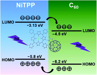
In order to well understand the excellent photodetection performances of the manufactured NiTPP-C60 photodetector, a possible mechanism is proposed here. According to the HOMO–LUMO values of C60 and NiTPP,23,59 the energy level diagram of the NiTPP-C60 intramolecular heterojunction is shown in Fig. 7. When the NiTPP-C60 device was exposed to light, both NiTPP and C60 could absorb photons to generate excitons, which quickly dissociated to electrons and holes. The electrons in NiTPP LUMO spontaneously transferred to the LUMO of C60, while the holes remain in the HOMO. The holes generated in C60 spontaneously transferred to the HOMO of NiTPP, while the electrons remained in the LUMO. Under an external electric field, electrons generated by light excitation in the D–A molecules can be quickly absorbed by C60 and drift rapidly in the highly crystalline microwires to the negative electrode, and holes move along the NiTPP to the positive electrode, thus forming photocurrent, which effectively prevent the recombination of excitons.
3. Conclusion
In summary, a fullerene molecular broadband photodetector was successfully constructed through molecular engineering. The addition of a nickel porphyrin onto the fullerene cage not only broadens the absorption range, but also promotes effective and fast charge carrier transfer. Large-area single-crystal arrays of NiTPP-C60 are realized by the liquid bridge induced assembly method, which makes the fabrication of integrated devices possible. The NiTPP-C60 broadband photodetector exhibited superior performances, mainly a fast response (350 nm: τon < 0.09 s; 425 nm: τon < 0.10 s; 530 nm: τon < 0.08 s) and high responsivity (350 nm: 8.92 A W−1, 425 nm: 11.6 A W−1, 530 nm: 3.11 A W−1), which are attributed to the high crystallinity, ordered molecular arrangement, efficient exciton dissociation and excellent charge carrier transport properties. This work brings ideas for the design of fullerene-based large-scale broadband photodetectors. By extending the conjugation length of porphyrin, the absorption would be extended from the visible to the NIR region. We believe that molecular engineering represents a general strategy for the preparation of molecules needed for broadband photodetectors.4. Experimental section
Substrate pre-treatment
The SiO2 (300 nm)/Si substrate was soaked in a H2SO4/H2O2 (v/v = 3![[thin space (1/6-em)]](https://www.rsc.org/images/entities/char_2009.gif) :
:![[thin space (1/6-em)]](https://www.rsc.org/images/entities/char_2009.gif) 1) solution for three hours, cleaned with acetone, ethanol, and deionized water, respectively under ultrasonication for ten minutes, and then dried with argon. The treated substrate was immersed in octadecyl trichlorosilane (OTS) solution for half an hour and then dried with a xenon lamp.
1) solution for three hours, cleaned with acetone, ethanol, and deionized water, respectively under ultrasonication for ten minutes, and then dried with argon. The treated substrate was immersed in octadecyl trichlorosilane (OTS) solution for half an hour and then dried with a xenon lamp.
Preparation of NiTPP-C60, C60 and NiTPP solutions
1 mg, 2 mg and 4 mg NiTPP-C60 powder was dissolved in 2 ml of o-dichlorobenzene, respectively under ultrasonication for two hours, and then the solution was filtered to obtain clear NiTPP-C60 solutions with concentrations of 0.5 mg ml−1, 1 mg ml−1 and 2 mg ml−1, respectively. 0.5 mg ml−1, 1 mg ml−1 and 2 mg ml−1 solutions of C60 and NiTPP solutions were prepared by the same procedure.Preparation of C60, NiTPP and NiTPP-C60 microwire arrays
15 μl of each NiTPP-C60, C60 and NiTPP solution was gently dropped onto the treated SiO2/Si substrate. Then, a template was horizontally covered on the substrate to prepare a device, which was placed in an oven at 80 °C for 12 hours.Photoelectric measurements
A test platform is mainly composed of a probe station, Keithley 2611B source meter, Charge-coupled Device (CCD), display, light source, and TTL signal generator. A combination of the display and the monocular microscope with the CCD can magnify the image of the area between the electrodes of the photodetector, so that the probe can come into contact with the electrodes more accurately. The probe and the photodetector electrodes form a loop which is connected to the Keithley 2611B digital source meter. The source meter provides stable bias voltage and time counting, and collects photocurrent and dark current data of the devices. The TTL signal generator is used to output a square wave signal and connect the light source to control the switch of the light source to obtain data such as photocurrent rise/decay time. Specifically, in this experiment, the gate voltage (VGS) and the bias voltage (VDS) are both set to 10 V. The TTL signal generator was set to provide a square wave signal with a frequency of 0.0005 kHz, which controlled the light source to turn on and off for 1 second, and repeated the cycle.Conflicts of interest
There are no conflicts to declare.Acknowledgements
The financial support from the National Natural Science Foundation of China (Grant No. 21672076 and 21971077) and the Graduates’ Innovation Fund, Huazhong University of Science and Technology (No. 2020yjsCXCY029) is gratefully acknowledged. The authors acknowledge the facility support of the Analytical and Testing Center in Huazhong University of Science and Technology for all related measurements.Notes and references
- J. Clark and G. Lanzani, Nat. Photonics, 2010, 4, 438–446 CrossRef CAS
.
- T. Rauch, M. Böberl, S. F. Tedde, J. Fürst, M. V. Kovalenko, G. Hesser, U. Lemmer, W. Heiss and O. Hayden, Nat. Photonics, 2009, 3, 332–336 CrossRef CAS
.
- K.-J. Baeg, M. Binda, D. Natali, M. Caironi and Y.-Y. Noh, Adv. Mater., 2013, 25, 4267–4295 CrossRef CAS
.
- M. Kim, H.-J. Ha, H.-J. Yun, I.-K. You, K.-J. Baeg, Y.-H. Kim and B.-K. Ju, Org. Electron., 2014, 15, 2677–2684 CrossRef CAS
.
- S. Goossens, G. Navickaite, C. Monasterio, S. Gupta, J. J. Piqueras, R. Pérez, G. Burwell, I. Nikitskiy, T. Lasanta, T. Galán, E. Puma, A. Centeno, A. Pesquera, A. Zurutuza, G. Konstantatos and F. Koppens, Nat. Photonics, 2017, 11, 366–371 CrossRef CAS
.
- G. Xiong, T. Minghong, X. Yangjun, C. Wanzhu, M. Ji Sun, C. Yong, Y. Gang, S. Chan-Long, N. Boo and J. H. Alan, Science, 2009, 325, 1665–1667 CrossRef
.
- S. Yang, N. Zhao, L. Zhang, H. Zhong, R. Liu and B. Zou, Nanotechnology, 2012, 23, 255203 CrossRef
.
- J. Qi, L. Ni, D. Yang, X. Zhou, W. Qiao, M. Li, D. Ma and Z. Y. Wang, J. Mater. Chem. C, 2014, 2, 2431–2438 RSC
.
- A. Armin, M. Hambsch, I. K. Kim, P. L. Burn, P. Meredith and E. B. Namdas, Laser Photonics Rev., 2014, 8, 924–932 CrossRef CAS
.
- Z. Chen, Z. Cheng, J. Wang, X. Wan, C. Shu, H. K. Tsang, H. P. Ho and J.-B. Xu, Adv. Opt. Mater., 2015, 3, 1207–1214 CrossRef CAS
.
- Y. Tao, X. Wu, W. Wang and J. Wang, J. Mater. Chem. C, 2015, 3, 1347–1353 RSC
.
- M. Buscema, D. J. Groenendijk, S. I. Blanter, G. A. Steele, H. S. J. van der Zant and A. Castellanos-Gomez, Nano Lett., 2014, 14, 3347–3352 CrossRef CAS
.
- W. Deng, J. Jie, Q. Shang, J. Wang, X. Zhang, S. Yao, Q. Zhang and X. Zhang, ACS Appl. Mater. Interfaces, 2015, 7, 2039–2045 CrossRef CAS
.
- W. Choi, M. Y. Cho, A. Konar, J. H. Lee, G.-B. Cha, S. C. Hong, S. Kim, J. Kim, D. Jena, J. Joo and S. Kim, Adv. Mater., 2012, 24, 5902 CrossRef
.
- G. Li, T. Guo, H. Zhang, H. Gao, J. Zhang, B. Liu, S. Yuan, G. Kai and X. Dong, Appl. Opt., 2007, 46, 283–286 CrossRef CAS
.
- S. D. Stranks and H. J. Snaith, Nat. Nanotechnol., 2015, 10, 391–402 CrossRef CAS
.
- L. Gao, K. Zeng, J. Guo, C. Ge, J. Du, Y. Zhao, C. Chen, H. Deng, Y. He, H. Song, G. Niu and J. Tang, Nano Lett., 2016, 16, 7446–7454 CrossRef CAS
.
- X. Zhang, J. Jie, W. Deng, Q. Shang, J. Wang, H. Wang, X. Chen and X. Zhang, Adv. Mater., 2016, 28, 2475–2503 CrossRef CAS
.
- A. K. Hailey, S.-Y. Wang, Y. Chen, M. M. Payne, J. E. Anthony, V. Podzorov and Y.-L. Loo, Adv. Funct. Mater., 2015, 25, 5662–5668 CrossRef CAS
.
- W. Deng, X. Zhang, L. Wang, J. Wang, Q. Shang, X. Zhang, L. Huang and J. Jie, Adv. Mater., 2015, 27, 7305–7312 CrossRef CAS
.
- S. Zheng, X. Xiong, Z. Zheng, T. Xu, L. Zhang, T. Zhai and X. Lu, Carbon, 2018, 126, 299–304 CrossRef CAS
.
- L. Wei, J. Yao and H. Fu, ACS Nano, 2013, 7, 7573–7582 CrossRef CAS
.
- L. Du, X. Luo, F. Zhao, W. Lv, J. Zhang, Y. Peng, Y. Tang and Y. Wang, Carbon, 2016, 96, 685–694 CrossRef CAS
.
- X. Zhao, T. Liu, H. Liu, S. Wang, X. Li, Y. Zhang, X. Hou, Z. Liu, W. Shi and T. J. S. Dennis, ACS Appl. Mater. Interfaces, 2018, 10, 42715–42722 CrossRef CAS
.
- G. Wei, Z. Lu, Y. Cai and C. Sui, Mater. Lett., 2017, 201, 137–139 CrossRef CAS
.
- B. Cai, Y. Su, J. Hu, C. Zou and Y. Zhang, J. Mater. Chem. C, 2018, 6, 1715–1721 RSC
.
- L. Zheng, T. Zhu, W. Xu, L. Liu, J. Zheng, X. Gong and F. Wudl, J. Mater. Chem. C, 2018, 6, 3634–3641 RSC
.
- P. Peumans, S. Uchida and S. R. Forrest, Nature, 2003, 425, 158–162 CrossRef CAS
.
- X.-J. Lu, C.-R. Zhang, J.-J. Gong, W. Wang, Z.-J. Liu, Y.-Z. Wu and H.-S. Chen, Spectrochim. Acta, Part A, 2020, 242, 118767 CrossRef CAS
.
- J. Roncali and I. Grosu, Adv. Sci., 2019, 6, 1801026 CrossRef
.
- S. Hedström, A. J. Matula and V. S. Batista, J. Phys. Chem. C, 2017, 121, 19053–19062 CrossRef
.
- R. S. Kularatne, H. D. Magurudeniya, P. Sista, M. C. Biewer and M. C. Stefan, J. Polym. Sci., Part A: Polym. Chem., 2013, 51, 743–768 CrossRef CAS
.
- M. Wolf, C. Villegas, O. Trukhina, J. L. Delgado, T. Torres, N. Martín, T. Clark and D. M. Guldi, J. Am. Chem. Soc., 2017, 139, 17474–17483 CrossRef CAS
.
- S. Vela, S. Bauroth, C. Atienza, A. Molina-Ontoria, D. M. Guldi and N. Martín, Angew. Chem., Int. Ed., 2016, 55, 15076–15080 CrossRef CAS
.
- M. Rudolf, L. Feng, Z. Slanina, T. Akasaka, S. Nagase and D. M. Guldi, J. Am. Chem. Soc., 2013, 135, 11165–11174 CrossRef CAS
.
- Y. Shao and Y. Yang, Adv. Mater., 2005, 17, 2841–2844 CrossRef CAS
.
- R. Charvet, Y. Yamamoto, T. Sasaki, J. Kim, K. Kato, M. Takata, A. Saeki, S. Seki and T. Aida, J. Am. Chem. Soc., 2012, 134, 2524–2527 CrossRef CAS
.
- Q. Xie, E. Perez-Cordero and L. Echegoyen, J. Am. Chem. Soc., 1992, 114, 3978–3980 CrossRef CAS
.
- D. M. Guldi, C. Luo, M. Prato, A. Troisi, F. Zerbetto, M. Scheloske, E. Dietel, W. Bauer and A. Hirsch, J. Am. Chem. Soc., 2001, 123, 9166–9167 CrossRef CAS
.
- S. MacMahon, R. Fong, P. S. Baran, I. Safonov, S. R. Wilson and D. I. Schuster, J. Org. Chem., 2001, 66, 5449–5455 CrossRef CAS
.
- H. Imahori and Y. Sakata, Eur. J. Org. Chem., 1999, 1999, 2445–2457 CrossRef
.
- D. M. Guldi, Chem. Commun., 2000, 321–327, 10.1039/A907807J
.
- C. Larsen, H. R. Barzegar, F. Nitze, T. Wågberg and L. Edman, Nanotechnology, 2012, 23, 344015 CrossRef
.
- X. Zhao, T. Liu, W. Shi, X. Hou, Z. Liu and T. J. S. Dennis, J. Phys. Chem. C, 2018, 122, 8822–8828 CrossRef CAS
.
- X. Zhao, T. Liu, Y. Zhang, S. Wang, X. Li, Y. Xiao, X. Hou, Z. Liu, W. Shi and T. J. S. Dennis, Adv. Mater. Interfaces, 2018, 5, 1800336 CrossRef
.
- K. Liu, S. Gao, Z. Zheng, X. Deng, S. Mukherjee, S. Wang, H. Xu, J. Wang, J. Liu, T. Zhai and Y. Fang, Adv. Mater., 2019, 31, 1808254 CrossRef
.
- B. Su, S. Wang, J. Ma, Y. Wu, X. Chen, Y. Song and L. Jiang, Adv. Mater., 2012, 24, 559–564 CrossRef CAS
.
- B. Su, S. Wang, Y. Wu, X. Chen, Y. Song and L. Jiang, Adv. Mater., 2012, 24, 2780–2785 CrossRef CAS
.
- Y. Wu, X. Chen, B. Su, Y. Song and L. Jiang, Adv. Funct. Mater., 2012, 22, 4569–4576 CrossRef CAS
.
- D. M. Guldi, I. Zilbermann, G. A. Anderson, K. Kordatos, M. Prato, R. Tafuro and L. Valli, J. Mater. Chem., 2004, 14, 303–309 RSC
.
- Z. Dai, Q. Ou, C. Wang, G. Si, B. Shabbir, C. Zheng, Z. Wang, Y. Zhang, Y. Huang, Y. Dong, J. J. Jasieniak, B. Su and Q. Bao, J. Mater. Chem. C, 2019, 7, 5954–5961 RSC
.
- Y. Zhao, X. Fan, J. Feng, X. Wang, Y. Wu, B. Su and L. Jiang, Adv.
Funct. Mater., 2018, 28, 1800470 CrossRef
.
- J. Feng, Q. Song, B. Zhang, Y. Wu, T. Wang and L. Jiang, Adv. Mater., 2017, 29, 1703143 CrossRef
.
- F. Wang, L. Jia, Y. Ding, H. Cai, W. Zheng and F. Huang, Small Methods, 2020, 4, 2000501 CrossRef
.
- H. Wang, Y. Zheng, R. Qin and J. Yu, J. Phys. D: Appl. Phys., 2018, 51, 104002 CrossRef
.
- N. A. Roslan, S. M. Abdullah, W. H. A. Majid and A. Supangat, Sens. Actuators, A, 2018, 279, 361–366 CrossRef CAS
.
- J. Miao, F. Zhang, M. Du, W. Wang and Y. Fang, Adv. Opt. Mater., 2018, 6, 1800001 CrossRef
.
- E.-P. Yao, B. J. Bohn, Y. Tong, H. Huang, L. Polavarapu and J. Feldmann, Adv. Opt. Mater., 2019, 7, 1801776 CrossRef
.
- C. He, Q. He, C. Deng, L. Shi, D. Zhu, Y. Fu, H. Cao and J. Cheng, Chem. Commun., 2010, 46, 7536–7538 RSC
.
Footnote |
| † Electronic supplementary information (ESI) available. See DOI: 10.1039/d0na00981d |
| This journal is © The Royal Society of Chemistry 2021 |

