DOI:
10.1039/D1NA00087J
(Paper)
Nanoscale Adv., 2021,
3, 4254-4270
Physico-chemical properties of selenium–tellurium alloys across the scales
Received
4th February 2021
, Accepted 28th May 2021
First published on 28th May 2021
Abstract
Selenium and tellurium are both energy critical elements as defined by the American Physical Society and the Materials Research Society. When mixed together, both elements form an alloy. The size- and shape-dependent thermal and optical properties of this alloy are investigated in this manuscript by using nano-thermodynamics and machine learning techniques. This alloy is found to have particularly interesting properties for solar cell applications.
1. Introduction
Selenium (Se) and tellurium (Te) are chalcogenide elements (i.e. they belong to the oxygen column in the periodic table) that have been classified as energy critical elements by the American Physical Society (APS) and the Materials Research Society (MRS).1,2 Se and Te are not abundant in the Earth's crust and they have crustal abundances of 0.130 ppm (ref. 3) and 0.001 ppm,4 respectively. Due to their scarcity, they cannot be mined directly and are recovered as by-products of copper refining.5 Due to the non-homogeneous geographic repartition of copper ores around the world, only a small number of countries have access to most of the world reserves of Se and Te (Fig. 1a and b) maintaining their prices above ∼$25 per kilogram (Fig. 1c). The worldwide consumption of Se and Te is illustrated in Fig. 1d and e. Specifically, Se is used essentially for metallurgy (30%), glass manufacturing (25%), agriculture (10%), chemicals (10%), electronics (10%) and some other minor uses (5%), while Te is used for solar cells (40%), thermoelectrics (30%), metallurgy (15%), rubber manufacturing (5%) and some other minor uses (10%). Currently, there is an increasing demand for Se to be used in copper–indium–gallium–diselenide (CIGS) solar cells6 and for Te to be used in cadmium telluride (CdTe) solar cells,7 making the domestic availability of these chalcogenide elements at risk. Se is now even added to CdTe to boost solar cell efficiency up to 22%.8 Se and Te are used in solar cells due to their energy bandgaps (1.79 and 0.33 eV, respectively),9 which allow them to absorb light in the visible and near infrared regions, respectively. A broadband solar absorber made exclusively of Te nanoparticles, with a size distribution ranging from 10 nm to 300 nm, has achieved more than 85% absorption of the solar radiation.10 Furthermore, Se is also used in lithium–selenium batteries for its electrical and electrochemical properties.11–13 Due to their low glass transition and crystallization temperatures, Se and Te are also widely used as phase change memory materials.14 Besides their use in electronics and optoelectronics, Se and Te are both used in medicine as antibacterial,15–17 antifungal,18 and anticancer drugs.19 For this type of application, the chalcogenide elements are synthesized as nanoparticles suspended in a solvent, consequently, forming a colloidal solution.18,20
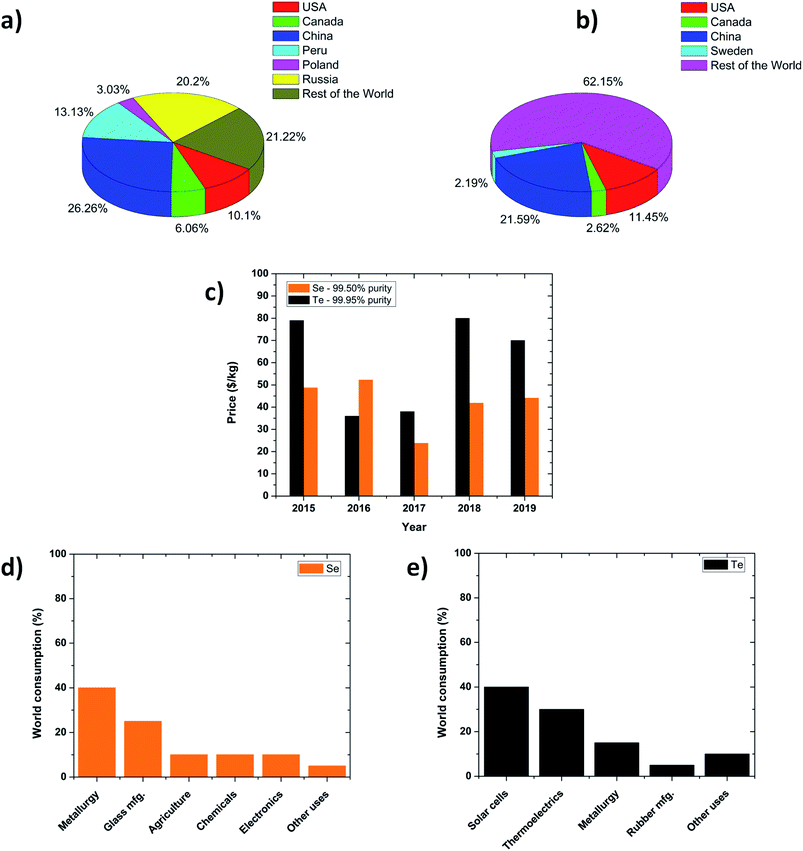 |
| | Fig. 1 World reserves of (a) selenium and (b) tellurium. The 2020 data come from the U.S. Geological Survey (USGS).80 (c) Price per kilogram of material as a function of time. The time period covers the last 5 years. World consumption of (d) selenium and (e) tellurium. All data come from the USGS.80 | |
Most of the scientific research regarding Se and Te has been focusing on each chemical element separately; however the two chemical elements can easily form an alloy, Se1−xTex, which allows a fine tuning of the physico-chemical properties through the control of its chemical composition. Relatively few papers have been published on this alloy and besides the chemical composition used to tune the physico-chemical properties of the Se1−xTex alloy, other variables such as size and shape were also studied. Indeed, Se1−xTex thin films,21–24 nanorods25 and nanowires26 were successfully prepared and characterized.
From a theoretical point of view, several techniques have been developed to predict the physico-chemical properties of alloys at the nanoscale. The Monte Carlo method was the first one to appear in the '40s,27 followed by molecular dynamics in the '50s,28 nano-thermodynamics in the '60s,29 and Density Functional Theory (DFT) in the '70s.30 Machine learning flourished in physical chemistry during the 2010's and grew as a separate field from artificial intelligence.31,32 Among those techniques, nano-thermodynamics is certainly the lesser known.33–38 It is only in 2001 that nano-thermodynamics was brought to broad daylight, due to an invited paper written by the pioneer of nano-thermodynamics “Terrence Hill” who published his ideas on thermodynamics of small systems in the first volume of Nano Letters.39,40 The ideas used in nano-thermodynamics allow the prediction of various material properties at the nanoscale such as phase diagrams.33,36,41
In this manuscript, nano-thermodynamics and machine learning techniques are used to predict the binary phase diagram, the surface segregation, Debye and Einstein temperature, glass and crystallization transition temperatures, and finally the optical properties including the bandgap, refractive index, dielectric constant, and exciton Bohr radius of Se1−xTex. All the thermal properties are discussed as a function of chemical composition while the optical properties are additionally discussed as functions of crystallinity. After presenting the theory, each result is discussed individually at the bulk- and nano-scales with respect to the available experimental data. Finally, the most important material properties of Se1−xTex are summarized in the conclusion.
2. Binary phase diagram
In order to understand the formation of Se1−xTex at the bulk scale, let's analyze the Hume-Rothery rules which are a set of basic rules that describe the conditions under which two chemical elements can form a solid solution.42 The rules state that an alloy forms if the chemical elements involved in the binary compound have similar crystal structures, similar electronegativity, similar valence, and a difference between their respective atomic radii less than 15%. According to Table 1, Se and Te have the same hexagonal crystal structure (hcp), the same valence (+6), similar electro negativities (∼6% difference), and a difference between their atomic radii of 14.6%, just below the 15% threshold, therefore satisfying all the conditions. Since all of these conditions are met, the bulk phase diagram of Se1−xTex should display complete miscibility across the entire temperature–composition space.43,44
Table 1 Bulk material properties of selenium (Se) and tellurium (Te)
| Material property |
Se |
Te |
Ref. |
|
Calculated by taking the average of the electron affinity and the 1st ionization energy.
Using value for a film with grain size greater than 1000 nm from ref. 58.
|
| Crystalline structure |
Hexagonal |
Hexagonal |
9
|
| Atomic radius (pm) |
117 |
137 |
9
|
| Valence |
+6 |
+6 |
9
|
| Electron affinity (eV) |
2.02 |
1.97 |
9
|
| 1st ionization energy (eV) |
9.7524 |
9.0096 |
9
|
| Mulliken electronegativitya (eV) |
5.88 |
5.50 |
|
|
a (pm) |
237 |
283 |
9
|
|
T
g,∞ (K) |
350 |
— |
43
|
|
T
m,∞ (K) |
494 |
723 |
9
|
| ΔHm,∞ (kJ mol−1) |
6.694 |
17.376 |
9
|
| ΔHvap (kJ mol−1) |
90 |
104.5 |
9
|
|
γ
l (J m−2) |
0.106 |
0.186 |
9
|
|
γ
s (J m−2) |
0.291 |
0.355 |
77 and 78 |
|
Ω
l (J mol−1) |
x
Se
x
Te[(−8271.5 + 8.78843T) + 467.8(xSe − xTe)] |
43
|
|
Ω
s (J mol−1) |
x
Se
x
Te(−222.6 − 1.2815T) |
43
|
|
Q
seg,∞ (kJ mol−1) |
−16.8 |
This work |
| η |
0.147 |
0.125 |
This work |
|
θ
D,∞ (K) |
150 |
141 |
79
|
|
θ
E,∞ (K) |
134 |
83b |
58 and 59 |
|
E
g (eV) |
1.79 |
0.33 |
9
|
|
μ (me) |
0.08 |
0.01775 |
This work |
To determine quantitatively the phase diagram of a binary alloy (A1−xBx), the composition (%) of the alloy in the liquid and solid states (xl, xs, respectively) has to be determined at each temperature T (K), while the total Gibbs free energy of the alloy, Gtotal (J mol−1), must be minimized. The total Gibbs free energy is given by the following equation:36
| | | Gtotal = xlGl(xB,T) + xsGs(xB,T) | (1a) |
where
xB (%) is the molar percent of element B in the alloy,
T (K) is the temperature.
Gl (J mol
−1) and
Gs (J mol
−1) are the Gibbs free energy of the liquid and solid phases, respectively, which are described by the following equations:
36| | Gl(xB,T) = RT[xB![[thin space (1/6-em)]](https://www.rsc.org/images/entities/char_2009.gif) ln ln![[thin space (1/6-em)]](https://www.rsc.org/images/entities/char_2009.gif) xB + (1 − xB)ln(1 − xB)] + ΩlxB(1 − xB) xB + (1 − xB)ln(1 − xB)] + ΩlxB(1 − xB) | (1b) |
| | Gs(xB,T) = RT[xB![[thin space (1/6-em)]](https://www.rsc.org/images/entities/char_2009.gif) ln ln![[thin space (1/6-em)]](https://www.rsc.org/images/entities/char_2009.gif) xB + (1 − xB)] + ΩsxB(1 − xB) + (1 − xB)ΔHAm(T/TAm − 1) + xBΔHBm(T/TBm − 1) xB + (1 − xB)] + ΩsxB(1 − xB) + (1 − xB)ΔHAm(T/TAm − 1) + xBΔHBm(T/TBm − 1) | (1c) |
where
R (8.314 J mol
−1 K
−1) is the ideal gas constant, Δ
HAm (J mol
−1) and Δ
HBm (J mol
−1) are the size-dependent melting enthalpies of elements A and B respectively,
TAm (K) and
TBm (K) are the size dependent-melting points of elements A and B respectively, and
Ωl (J mol
−1) and
Ωs (J mol
−1) are the size-dependent enthalpies of mixing for the liquid and solid state respectively.
For each temperature T, between the melting points of the two chemical elements (A ≡ Se and B ≡ Te) constituting the alloy, the compositions that minimize the total Gibbs free energy are determined. Therefore, at equilibrium, when the solid and liquid phases coexist (Gl = Gs), the solutions of eqn (1) form the solidus and liquidus curves in the binary phase diagram.
By using the bulk material properties of Se and Te listed in Table 1, the solidus–liquidus curves of Se1−xTex are displayed in Fig. 2a. The excellent agreement between the calculated bulk phase diagram and the experimental data points, Fig. 2a, proved that the phase diagram is described well by the sub-regular solution model (eqn (1)).
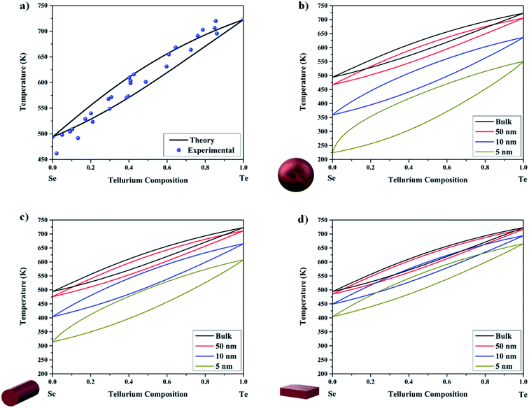 |
| | Fig. 2 (a) Binary phase diagram of the bulk Se1−xTex alloy displaying the solidus–liquidus curves (eqn (1)). Experimental data points are taken from ref. 81. Binary phase diagram for the Se1−xTex alloy displaying the solidus–liquidus curves (eqn (1) and (2)) at the nanoscale (50, 10 and 5 nm) for the (b) sphere, (c) wire, and (d) film morphologies. | |
To determine the binary phase diagram of Se1−xTex at the nanoscale, all the size-dependent material properties involved in eqn (1) have to be calculated. In order to evaluate those values, the following scaling law is used:36,45
| |  | (2) |
where

represents the size/shape effect on the material,
D is the characteristic size of the nanostructure,
A/
V is the surface to volume ratio (
Table 2), and
γs and
γl are the solid and liquid surface energy, respectively.
Tm,∞, Δ
Hm,∞,
Ωs,∞ and
Ωl,∞ are the bulk melting temperature, bulk melting enthalpy, and bulk enthalpy of mixing for the solid and liquid phase, respectively (
Table 1). The
αshape parameters for the sphere (
A/
V = 6/
D), infinitely long wire (
A/
V = 4/
D), and infinitely long and wide film (
A/
V = 2/
D) morphologies are given in
Table 2. The characteristic length,
D, for the sphere, infinitely long wire, and infinitely long and wide film are the diameter, diameter, and the thickness, respectively. As expected, the
αshape parameter increases with increasing value of the surface-to-volume ratio, which results in
αsphere >
αwire >
αfilm.
Table 2 Parameters quantifying the size effect on selenium (Se), tellurium (Te) and Se1−xTex for the sphere, wire, and film morphologies
| Shape |
α
Seshape (nm) |
α
Teshape (nm) |

|
| Sphere |
2.733 |
1.193 |
2.733 − 1.540x |
| Wire |
1.822 |
0.796 |
1.822 − 1.026x |
| Film |
0.911 |
0.398 |
0.911 − 0.513x |
At the nanoscale, the lens-shape of the solidus–liquidus curves is preserved, but shifted to lower temperatures when compared to the bulk phase diagram; see Fig. 2b–d. For all the morphologies considered (sphere, wire, and film), a broadening effect is noted; i.e. as the size is decreased, the temperature difference between the solidus and liquidus curves increases. This effect is related to the mixing enthalpy of the solid phase. Indeed, as the size decreases the mixing enthalpy of the solid phase increases, because the mixing enthalpy is negative all across the composition range; see Fig. 3. This indicates that the broadening effect should be observed in all binary alloys that have a negative mixing enthalpy at the bulk scale.
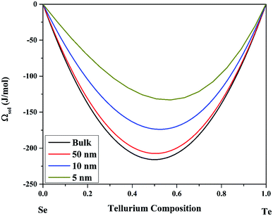 |
| | Fig. 3 Size-dependent enthalpy of mixing at 500 K for the solid solution of Se1−xTex alloy considering the spherical morphology. | |
It is important to note that nanoparticles undergo mainly two types of melting: homogeneous melting and heterogeneous melting.46 With the homogeneous melting, the solid particle is always at equilibrium with the melted one. With the heterogeneous melting, a liquid layer nucleates at the surface of the particle and grows with temperature; this is also called “surface melting”. Both types of melting predict a linear relationship between the melting temperature and the reciprocal size of the particle. Consequently, they can be described by eqn (2), but the value of αshape will be different in each case.46 Surface melting has already been observed in metallic gold nanoparticles by in situ transmission electron microscopy.47 The shape transformation of gold nanoparticles was caused by surface melting.48 However, here we are studying two semiconductors Se and Te which have a much smaller Hamaker constant compared to gold, consequently hindering surface melting.49 Therefore, no surface melting was considered in this manuscript.
3. Surface segregation
Shrinking the size of an alloy to the nanoscale is often accompanied by some surface segregation. Indeed, there is always a natural tendency between the two chemical elements that one of the two prefers to be at the surface. In the seventies, Williams and Nason50 predicted the surface segregation of binary compounds by describing the enrichment of the outermost layer of the material only. According to their model, the surface composition of the binary alloy is given by:50| |  | (3a) |
| |  | (3b) |
where xcoresolidus (%) and xcoreliquidus (%) are the size-dependent solidus and liquidus composition given by minimizing the Gibbs' free energy when no surface segregation effect is considered. ΔHvap (J mol−1) and ΔHsub (J mol−1) are the absolute difference between the two pure elements for the vaporization enthalpy and sublimation enthalpy, respectively. z1v/z1 is the ratio between the number of atoms in the vertical direction and the coordination number; those numbers are equal to 2 and 3, respectively, for the hexagonal structure of Se and Te.
Tománek et al.51 described surface segregation in terms of a surface segregation energy, representing the work involved in exchanging a surface atom with a core atom. This concept is described for a bulk material (eqn (4a)) and a nano material (eqn (4b)) by the following equations, respectively:51
| |  | (4a) |
| |  | (4b) |
where
xsurface (%) and
xcore (%) are the composition of the surface and the core of the material, respectively,
R (J mol
−1 K
−1) is the ideal gas constant, and
T (K) is the temperature.
Qseg,∞ (J mol
−1) and
Qseg (J mol
−1) are the surface segregation energy at the bulk and nanoscale, respectively. As surface segregation is also size-dependent, Guisbiers
et al.52 described the size effect on the surface segregation energy as:
| |  | (4c) |
By using the solidus data from Fig. 2b–d as the core composition within eqn (3a), the surface segregation in nanoparticles, wires, and films can be predicted (Fig. 4a–c). Indeed, Fig. 4a–c show the plot of the surface composition of the nanostructure, xsurface (%) versus its core composition, xcore (%). The x-axis of Fig. 4a–c can be understood as when the core composition is zero the structure is only made of Se, while when the core composition equals one, the structure is only made of Te. When the core composition varies between zero and one, the surface composition does not evolve linearly with the core composition anymore. As seen in Fig. 4a–c, Se segregates to the surface.
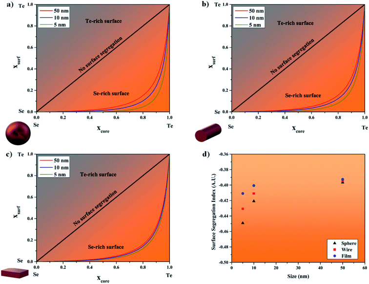 |
| | Fig. 4 Surface composition versus the core composition of the Se1−xTex alloy at the solidus temperature for the (a) sphere, (b) wire, and (c) film morphologies. (d) Surface segregation index as defined in ref. 53versus the size of the nanostructure. | |
The bulk surface segregation energy of Se1−xTex has been determined as −16.8 kJ mol−1, by equaling eqn (4a) to eqn (3a). The value reported here is comparable to the surface segregation energy reported for Bi1−xSbx,53 −15.7 kJ mol−1, and for Ni1−xPdx,51 −16.8 kJ mol−1. In those alloys, it was demonstrated that Bi and Pd were the chemical elements segregating preferentially to the surface of Bi1−xSbx, and Ni1−xPdx, respectively. The surface segregation is enhanced as the surface-to-volume ratio increased.
According to Guisbiers et al.,54 in the case of total miscibility the material with the highest melting point should segregate to the surface, but this is not the case in Se1−xTex. When developing their rules, they only considered face centered cubic (f.c.c.) alloy systems; therefore, due to the hexagonal crystal structure of Se1−xTex, it does not follow the rules described in ref. 54. This suggests that the rules need to be revised when considering hexagonal crystal systems.
In Fig. 4d, the Surface Segregation Index (SSI) of Se1−xTex is calculated versus the size of the structure. The SSI was defined in ref. 53, as the surface area between the no segregation line and the segregated line in a plot displaying the surface composition versus core composition (Fig. 4a–c). When SSI is negative, Se is found to be preferentially at the surface while when SSI is positive, Te is found preferentially at the surface. This index helps to quantify the intensity of the surface segregation. The SSI becomes more negative as the size of the Se1−xTex structure decreases. In absolute value, the sequence SSIsphere > SSIwire > SSIfilm is observed because αsphere > αwire > αfilm.
4. Debye and Einstein temperatures
The bulk Debye temperature, θD,∞ (K) is the temperature of a material's highest normal mode of vibration, i.e., the highest temperature that can be achieved due to a single phonon.55| |  | (5) |
where ℏ is the reduced Planck's constant (J Hz−1), kB is the Boltzmann's constant (J K−1) and ωD (Hz) is the maximal phonon frequency of the bulk material. The Debye temperature indicates the approximate temperature limit below which quantum effects may be observed.
The Debye temperature is closely related to the melting temperature through Lindeman's melting criterion.56,57 Indeed, according to Lindeman, solids liquefy when the amplitude of vibration exceeds a fraction of the interatomic spacing. The modern form of Lindeman's criterion is given by:57
| |  | (6) |
where
η is the Lindeman coefficient,
ξ = 2.29 × 10
20 mol J
−1 K
−1 s
−1,
A is the atomic mass, and
α is the interatomic distance. From the data listed in
Table 1, the Lindeman coefficients of Se and Te were determined at 0.147 and 0.125, respectively.
From Lindeman's criterion, the square of the Debye temperature is directly proportional to the melting temperature i.e. θD,∞2 ∝ Tm,∞. Assuming that this relationship holds at the nanoscale, then we have:45,55
| |  | (7) |
The bulk Einstein temperature, θE,∞ (K) characterizes a bulk solid composed of single-frequency quantum harmonic oscillators. All the atoms are supposed to oscillate at the same frequency, called Einstein frequency, ωE,∞ (Hz). Einstein's single frequency can be viewed as a kind of mean value of all the frequencies available in the Debye model. The bulk Einstein's temperature is defined as:55
| |  | (8) |
As the Debye temperature and the Einstein temperature are proportional to each other, we consequently have:55
| |  | (9) |
In Fig. 5, the Debye and Einstein temperatures of Se and Te nanostructures are plotted using eqn (10). The available experimental data are extracted from ref. 58 and 59 and used for comparison with the theoretical curves. As it can be seen in Fig. 5a, c and d, the theoretical curves are in good agreement with the available experimental data. In Fig. 5b, the theoretical curves are displayed without comparison to experimental data because the Debye temperature of Te nanostructures has not been reported yet at the nanoscale.
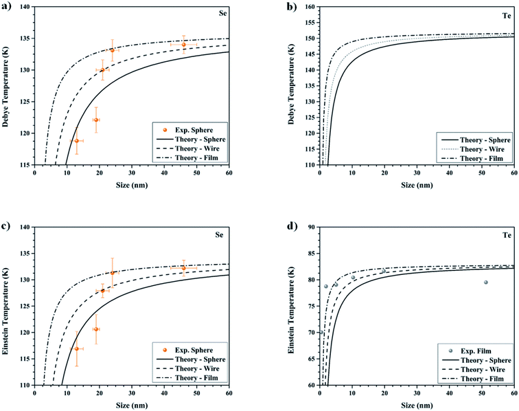 |
| | Fig. 5 Debye temperature versus the size of (a) Se nanostructures, (b) Te nanostructures. Einstein temperature versus the size of (c) Se nanostructures, (d) Te nanostructures. Experimental data for (a) and (c) are from ref. 59 for spherical nanoparticles, and (d) from ref. 58 for Te films. | |
Furthermore, in an alloy like Se1−xTex, the Debye temperature becomes composition dependent i.e. Se1−xTex. Some evidence of composition dependence for the Debye Temperature of Se1−xTex is found in ref. 60 and 61. In order to evaluate this temperature, the melting temperature in eqn (8) is substituted by the solidus temperature of the alloy. It is assumed that the material's molar volume varies with Vegard's law since the material's crystalline indices vary linearly throughout the entire composition range.43
Fig. 6 shows how the Debye temperature varies with increasing Te composition for the bulk, sphere, wire, and film morphologies in (a), (b), (c) and (d), respectively. Fig. 6a is obtained by using eqn (7). This shows that the Debye temperature varies non-linearly between pure Se and pure Te with that of Te being lower and that of Se being higher. When the size effect is applied, Fig. 6b–d, this changes significantly. At sizes around 10 nm for the spherical morphology, the Debye temperatures for pure Se and Te become almost equal, and below this size a tilting effect is noted, i.e., the Debye temperature of Se is now lower and that of Te is higher.
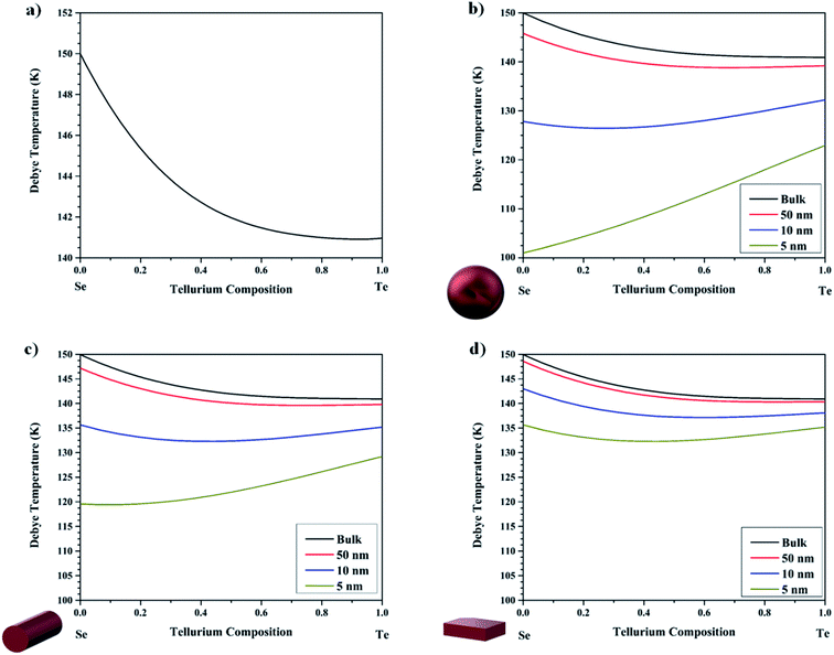 |
| | Fig. 6 Compositionally dependent Debye Temperature for the Se1−xTex alloy in the (a) bulk, and the (b) sphere, (c) wire, and (d) film morphologies. | |
5. Glass and crystallization temperatures
Depending on the kinetics of the cooling process, a solid may have two solidification paths, the crystallization path and the glass transition path. Indeed, the crystallization path displays the transition from a liquid into a crystalline solid which occurs at the melting temperature, Tm,∞; while the glass transition path displays the transition from a liquid into an amorphous solid which occurs at the glass temperature, Tg,∞. Glass formation is a matter of bypassing crystallization by cooling down the liquid “fast enough” and “far enough”. “Far enough” means that the cooling temperature must be well below the glass temperature of the material (T < Tg,∞). “Fast enough” means that the cooling process to bring the liquid from a temperature Tm,∞ to a temperature T lower than Tg,∞ must be performed in a timeframe shorter than the crystallization time. Fig. 7a shows the process by which a material either becomes a glass or a crystal based on the volume of the material. As seen in Fig. 7b, there is some discrepancy in the data collected from ref. 24 and 43 in the measurement of the glass and crystallization temperatures of Se1−xTex alloys, which is due to the heating rate used in the experiments. Generally, when a slower heating rate is used the crystallization occurs at a lower temperature.
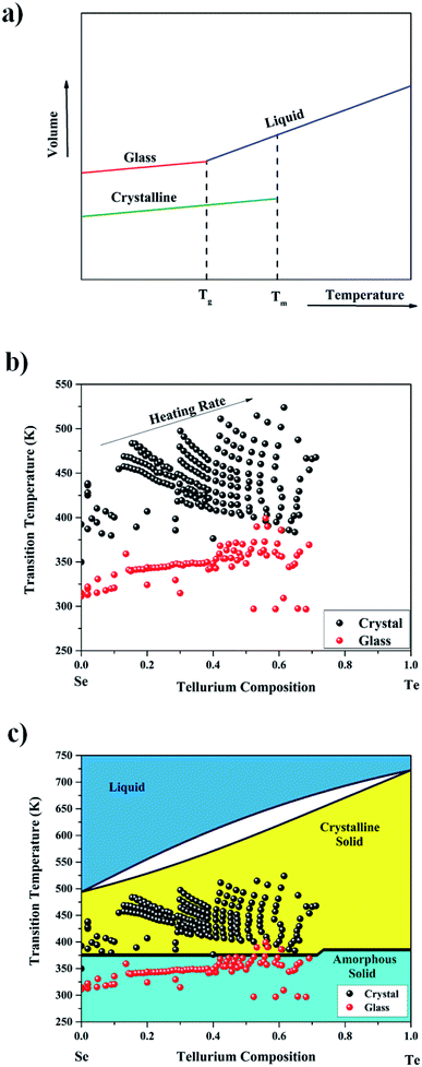 |
| | Fig. 7 (a) Sketch representing the two possible scenarios for solidification, the crystallization path and the glass transition path. (b) Experimental data are from ref. 24, which were extracted by using the online tool WebPlotDigitizer,82 and ref. 43. (c) Logistic regression classifier shows the boundary between the crystalline region and the amorphous region. Below this temperature, one should expect a glass transition; but above this temperature, one should expect a crystalline transition. | |
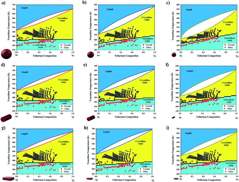
Prediction of glass temperature in an alloy is still an open question in materials science since no analytical or ab initio model can predict it accurately.62 Therefore, machine learning techniques have been used to predict the transition temperature.62 The points (composition, temperature) within the phase diagram underwent a binary classification allowing machine learning techniques to determine precisely the glass/crystallization boundary all across the phase diagram. Glass transition and crystallization were represented by 0 or 1, respectively. A logistic regression classifier was used to predict the region where the glass transition or crystallization would be likely to occur. Logistic regression was chosen as it is simple and has been applied widely in many fields.31 It was implemented in python code utilizing the sklearn library.63 The model validation was performed by choosing the model fitting parameters that resulted in the highest accuracy. In Fig. 7c, the output of the logistic regression model for the bulk Se1−xTex alloy is presented. From this figure, it is easy to see that the points above the line, in yellow, indicate the crystalline phase. Below this line, in cyan, the points represent the glass phase across the entire composition range. The model produced is simple and it is easily interpretable. Obviously, other models may produce a tighter fit on the data (K-Nearest Neighbors64 or Artificial Neural Networks65), but these methods are difficult to interpret and generally overfit the data. This method gives a range of temperatures that experimentalists should investigate in order to detect a possible transition to the crystalline phase from the glassy one or from the liquid to the glass.
Like any other material property, the glass temperature is also size and shape-dependent.55 It has been shown theoretically by Jiang et al.55 and confirmed experimentally by Guisbiers et al.66 that glass temperatures follow this type of scaling law:
| |  | (10) |
where
Tg (K) is the size/shape-dependent glass temperature and
Tg,∞ (K) is the bulk glass temperature. Following a reheating of the glassy material, crystallization may occur. Crystallization temperatures,
Tc,∞ (K), are always higher than the glass transition temperature of the material while also being lower than the melting temperature. Consequently, the crystallization temperature should follow the same trend as the melting temperature when looking at size and shape effects at the nanoscale,
i.e.,
| |  | (11) |
where
Tc (K) is the size/shape dependent crystallization temperature and
Tc,∞ (K) is the bulk crystallization temperature.
Fig. 8 shows the same analysis as above but on the nanoscale counterpart. The data in this analysis were generated by applying the scaling laws (eqn (11) and (12)) to each data point. It is noted that as the size of the structure is decreased, the boundary starts tilting more towards the Se rich parts of the alloy, due to the much larger αshape parameter of Se compared to Te.
 |
| | Fig. 8 (a, b, and c) Nano-sized glass (yellow) and crystalline (cyan) phases for spherical particles with sizes of 50 nm, 10 nm, and 5 nm, respectively. (d, e, and f) Nano-sized glass (yellow) and crystalline (cyan) phases for wire morphologies with sizes of 50 nm, 10 nm, and 5 nm, respectively. (g, h, and i) Nano-sized glass (yellow) and crystalline (cyan) phases for films with sizes of 50 nm, 10 nm, and 5 nm, respectively. | |
6. Glass forming ability
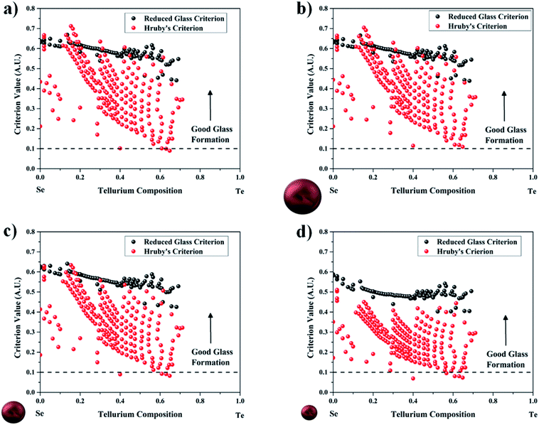
Glass formation and glass stability are interesting properties of amorphous materials to study, and here we have described two criteria that we used to evaluate the Se1−xTex system. The ability of a material to form a glass during solidification has been termed the Glass-Forming Ability (GFA). One of the earliest criteria to determine the GFA was by using the reduced glass transition temperature defined as the ratio between the glass temperature and the melting temperature (the melting temperature is substituted by the liquidus temperature in the case of an alloy). Reduced glass transition is typically correlated with GFA or the minimum cooling rate to cause a glass to form. The results here are supported by the results for the cooling rates reported in ref. 24 where samples' minimum cooling rates evolved linearly with increase in Te composition. This implies that low reduced glass transition values correspond to very high cooling rates, leading to low GFA; see Fig. 9a. It is defined by the following equation:| |  | (12) |
 |
| | Fig. 9 Reduced glass criterion and Hruby's criterion for the (a) bulk, and spherical particle morphologies with sizes equal to (b) 50 nm, (c) 10 nm, and (d) 5 nm. Typically, those with a value greater than 0.1 in the Hruby's criterion are good glass formers. | |
The reduced glass transition temperature, Trg, is a unitless number varying between 0 and 1. It has been found to be a good indicator of GFA, i.e. the higher its value, the easier it is to form a glass. Turnbull suggested that at Trg ≥ 2/3, the crystallization is suppressed.67 The reduced glass transition temperature considers only the Glass Forming Ability (GFA) but does not consider the Glass Stability (GS). Many other criteria exist in the literature to determine the GFA.68,69 In order to consider GFA and GS at the same time, there is the Hruby's criterion:14,70
| |  | (13) |
Hruby's criterion tells a similar story for the bulk material, Fig. 9a. This criterion is different from the reduced glass transition by being more sensitive to the crystallization temperature and not just the glass and liquidus temperatures. This is evident when investigating the samples where Te composition is above 0.4. Indeed, large spread in the data reveals sharp dips towards difficult glass formation, i.e., below 0.1 in Hruby's criterion.
At the nanoscale, a similar story to that at the bulk scale is noticed. However, there is a burning question at the nanoscale: does having a nano-sized material help stabilize the glass phase? The results plotted in Fig. 9b–c for the spherical nanoparticles with sizes of 50 nm, 10 nm, and 5 nm do not support the claim that glass formation is more difficult at the nanoscale. Indeed, most of the data points stay above 0.1 threshold in Hruby's criterion, but the data underwent simply an overall shift downward. Physically this can be understood as when the size decreases, the number of particles in the system also decreases, which means that the number of degrees of freedom in the system is less in comparison to the bulk; and as such the number of possible movements that are available upon moving to a lower size are not there, i.e., lower entropy in the nano-system.
7. Optical properties
At room temperature, Se1−xTex is a semiconductor all over its entire composition range. Therefore, it is interesting to look at the optoelectronic properties of this alloy as a function of its chemical composition, size, and shape. At the bulk scale, the optoelectronic properties of Se1−xTex are well understood; however, very little is known regarding this material at the nanoscale.
At the bulk scale, the energy bandgap of Se1−xTex follows Vegard's law:71
| | | ESe–Teg(x) = (1 − x)ESeg + xETeg + bx(1 − x) | (14) |
where
ESe–Teg(
x) is the energy bandgap of Se
1−xTe
x at the composition
x.
ESeg (eV) and
ETeg (eV) are the energy bandgap of Se and Te, respectively.
b is the bowing parameter. The data gathered from ref.
21 suggest that
b equals zero (
i.e. bamorphous = 0) when Se
1−xTe
x is amorphous, and as such its energy bandgap exhibits a linear dependence with respect to the chemical composition,
x (
Fig. 10a). When Se
1−xTe
x is crystalline, its energy bandgap does not follow a linear trend anymore but displays bowing characterized by the following bowing factor,
bcrystalline = 1.102.
72 When crystalline, Se and Te have slightly different energy bandgap values as seen in ref.
72, 1.73 and 0.35 eV, respectively, due to the change in their lattice parameter. As a note, glassy or amorphous Se
1−xTe
x has not been reported for compositions greater than 80%, due to not high enough cooling rates when transitioning from the liquid to the glassy state.
24 For the crystalline phase, the material is reported to exist across the entire composition as seen in ref.
72. Also in that reference, they reported the energy bandgap of the crystalline phase to exhibit some bowing. The energy bandgaps of the amorphous and crystalline phases are consequently given by:
| | | Ea-SeTeg,∞(x) = 1.84 − 1.50x | (15a) |
| | | Ec-SeTeg,∞(x) = 0.35x + 1.73(1 − x) − 1.102x(1 − x) | (15b) |
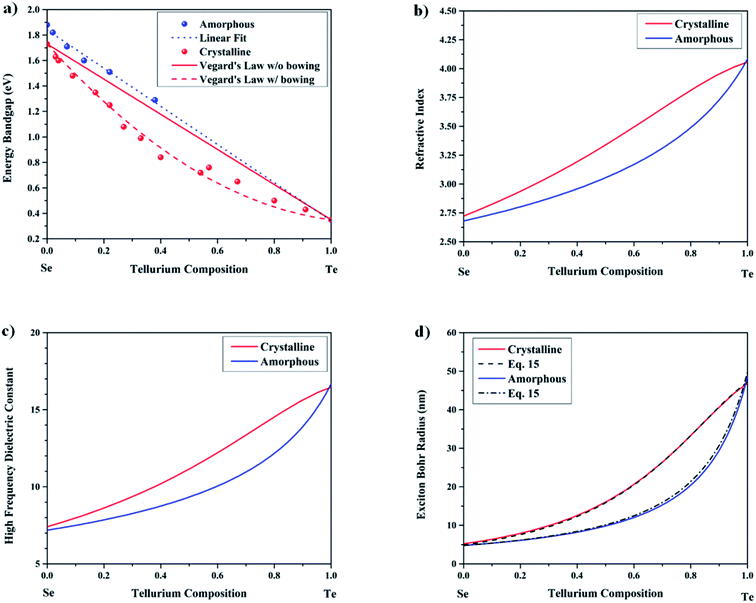 |
| | Fig. 10 (a) Energy bandgap versus the Te composition of the bulk Se1−xTex alloy. Experimental data points taken from ref. 21 for the amorphous case and ref. 72 for the crystalline case. (b) Refractive index versus the Te composition for the amorphous and crystalline cases. (c) High-frequency dielectric constant versus the Te composition for the amorphous and crystalline cases. (d) Exciton Bohr radius versus the Te composition calculated according to ref. 73 for the amorphous and crystalline cases, and curve fitting by eqn (17) using the calculated high-frequency dielectric constant from Fig. 8c and assuming a linear exciton effective mass for the amorphous case and Vegard's law like with bowing for the crystalline case. | |
From this and with eqn (16a) and (16b), respectively, the refractive index and high-frequency dielectric constant are plotted in Fig. 10b and c, respectively. The refractive index (16a) and high-frequency dielectric constant (eqn (16b)) of Se1−xTex (ref. 73) are modelled using the following:
| | | nSe–Te(x) = k1/4[ESe–Teg(x)]−1/4 | (16a) |
| | | εSe–Te∞(x) = [nSe–Te(x)]2 | (16b) |
where
εSe–Te∞(
x) and
nSe–Te(
x) are the high-frequency dielectric constant and refractive index of Se
1−xTe
x at a composition
x, respectively.
k is a constant equal to 95 eV. By using
eqn (16a) and
(16b), the refractive index and high frequency dielectric constant of Se
1−xTe
x can be determined as a function of the chemical composition of the alloy.
The exciton Bohr radius is a measure of when a material becomes quantum confined and is expressed as follows:73
| |  | (17) |
where
εSe–Te∞(
x) is the high-frequency dielectric constant of Se
1−xTe
x,
me is the rest mass of an electron, 9.11 × 10
−31 kg,
a0 is the atomic Bohr radius, 0.053 nm, and
μ(
x) is the exciton reduced mass given by

where

and

are the effective mass of the electron and hole, respectively.
The exciton Bohr radius of Se1−xTex can be calculated by using the relationship between the exciton Bohr radius and the energy bandgap established in ref. 73:
| | log[aSe–TeB,ex(x)] = ξ + η![[thin space (1/6-em)]](https://www.rsc.org/images/entities/char_2009.gif) log[ESe–Teg,∞(x)] log[ESe–Teg,∞(x)] | (18) |
where
aSe–TeB,ex(
x) and
ESe–Teg,∞(
x) are the exciton Bohr radius and the bulk energy bandgap of Se
1−xTe
x at a composition
x, respectively.
ξ and
η are the fitting parameters given as 1.04434 ± 0.04976 and −1.37696 ± 0.10488, respectively.
73Fig. 10d shows the amorphous and crystalline exciton Bohr radius as given by
eqn (18). The exciton Bohr radius of a semiconductor material is of primary importance to determine the onset of quantum confinement effects. By using
eqn (17) and
(18), the material's exciton reduced mass,
μ(
x), was determined. In order to achieve this, the exciton reduced mass was assumed to vary linearly with the composition, which seems reasonable based on the data gathered from ref.
74. Indeed, Beyer
et al. determined experimentally from conductivity measurements that the hole reduced mass varied linearly. Adopting this allows for good fitting found in comparison to
eqn (17) (
Fig. 9d). The exciton reduced masses for the amorphous and crystalline states are consequently described by:
| | | μa-SeTe(x) = 0.01775x + 0.08(1 − x) | (19a) |
| | | μc-SeTe(x) = 0.0185x + 0.08(1 − x) − 0.048x(1 − x) | (19b) |
By increasing the Te composition, the reduced mass of Se1−xTex decreases. The exciton effective mass for the pure amorphous and the crystalline structures of Se is 0.080me while the exciton effective mass of crystalline Te is 0.019me. According to Beyer et al.,74 a fairly heavy hole effective mass, evolving as  , is expected in Se1−xTex alloys. A large hole effective mass is common in some material systems such as Si and GaN,73 where it is shown that it makes a very low contribution to the quantum confinement of those structures. This is very apparent by examining Te on its own which has a very large hole effective mass, 1.4me. In contrast, Se has a much smaller hole effective mass, commonly found in semiconductor systems (i.e., AlN, AlP, AlAs, InN, InP, InAs), consequently showing contributions from both the hole and the electron in the exciton effective mass. This suggests that there is a strong change in the band structure of this alloy. Further theoretical studies using DFT and experiments using Angle Resolved Photo-Electron Spectroscopy (ARPES) should be performed to provide a better insight into the band structure of Se, Te, and Se1−xTex. These studies are out of the scope of this paper.
In order to determine the energy bandgap of Se1−xTex at the nanoscale, the following scaling law is used:36
| |  | (20) |
where
ESe–Teg,∞ and
ESe–Teg are the bulk and size-dependent energy bandgaps of Se
1−xTe
x at a fixed composition,
x. In the case of an alloy,
αshape(
x) becomes composition-dependent.
Eqn (20) is valid for sizes larger than the exciton Bohr radius of the material.
36
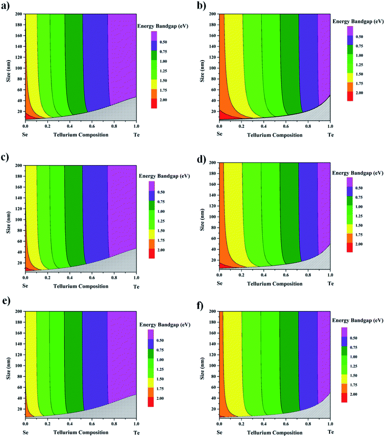
By using eqn (20), the energy bandgap of Se1−xTex as a function of its chemical composition and size can be calculated and it is illustrated in Fig. 11 for the sphere, wire, and film morphologies. The region where the size is below the exciton Bohr radius, is indicated in grey in Fig. 11. The sphere displays the largest size effect compared to the wire and the film because αsphere > αwire > αfilm; see Table 2. In order to use those nanostructures in solar cells, it has been demonstrated by Zdanowicz et al.75 that the best energy bandgap to absorb the solar light was ∼1.39 eV for a cell having only one single absorbing material. Therefore, the green areas in Fig. 11 are the most adequate regions to select the nanostructures from. This region corresponds to a chemical composition of Te varying between 20 and 40%. Above ∼2 eV, the region in red in Fig. 11 represents the nanostructures that could be used in wide-bandgap semiconductor applications such as biological and chemical sensors.76 Special consideration should be given to the crystallinity (crystalline or amorphous) and morphology (sphere, wire, and film) when selecting materials for this purpose. From Fig. 11, it is clear that nanoparticles are best for wide-bandgap semiconductor applications by comparison to wires or films. Indeed, wires and films only appear to be the right material properties to cater to these applications at very small sizes, i.e., below 20 nm, and below 20% Te composition.
 |
| | Fig. 11 Contour plots displaying the energy bandgap of the Se1−xTex alloy versus the Te composition and size of the alloy in crystalline and amorphous states for the (a and b) sphere, (c and d) wire, and (e and f) film morphologies. Areas in grey are the respective exciton Bohr radii for the crystalline and amorphous phases. | |
8. Material selection for solar cell technology
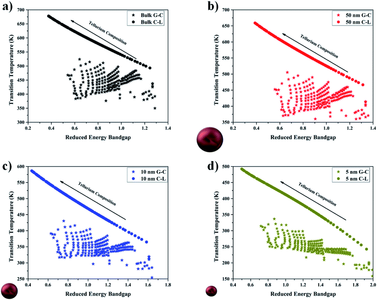
Fig. 12a–d show the transition temperature versus the reduced bandgap energy of Se1−xTex alloys at various sizes (bulk, 50 nm, 10 nm, and 5 nm). The reduced bandgap energy is defined as the observed energy bandgap divided by the target bandgap, which results in the optimal value being 1. For a glassy material, the crystalline temperature is used as the transition temperature since a material should remain in the glassy state unless the temperature is above the crystalline transition temperature. For crystalline materials, the liquidus temperature is used as the transition temperature. This kind of plot elucidates which materials and under which conditions it might be appropriate to use bulk or nanoparticle morphologies for solar cell technologies. As stated previously, an energy bandgap around 1.39 eV has been shown to be the optimal bandgap for a material to harvest solar energy. Due to this, a large number of Te-rich alloys would not be advantageous to use for these goals as they predominately have bandgaps bellow 1.39. However, this may not be a hard and fast rule for material selection as shown in ref. 10 wherein by using a broad range of sizes of Te nanoparticles they were able to absorb 85% of the solar spectrum. Another condition that is necessary to impose is that of the transition temperature; if a material undergoes a phase change then the material properties change which results in the material becoming something else. For example, for a bulk Se0.6Te0.4 material, the bandgap energy of the crystalline state is 0.84 eV, while the amorphous phase has a bandgap of 1.23 eV, which results in a difference of ∼0.4 eV. This kind of transition does not bode well for any material system that relies on a specific material property. Solar cells typically operate between 20 °C and 50 °C, so a material should not experience a transition in this window. This condition limits our search to particles with sizes above 10 nm and with compositions around 0.3.
 |
| | Fig. 12 Transition temperature vs. reduced energy bandgap of the amorphous (stars) and crystalline (circles) phases for the (a) bulk and nano-sized spherical nanoparticles with sizes equal to (b) 50 nm, (c) 10 nm, and (d) 5 nm. | |
9. Conclusions
In conclusion, the thermal and optoelectronic properties of Se1−xTex alloys are investigated and discussed. It is found that the properties are strongly size-dependent, i.e., both Se and Te have large αshape parameters. Se naturally segregates preferentially at the surface of the alloy at the nanoscale. The surface segregation energy has been determined at the bulk scale to be equal to −16.8 kJ mol−1. Debye and Einstein temperatures of Se, Te, and Se1−xTex were investigated and were found to be in good agreement with the model proposed here in. Additionally, a logistic regression model was introduced to determine where the boundary between amorphous and crystalline states is. This model was extended to the nanoscale through nano-thermodynamics. The exciton Bohr radius of Se1−xTex increases with the Te composition. Se1−xTex nanostructures with a Te composition ranging between 20 and 40% are the most adequate structures to be used in solar cells.
Data availability
The data that support the findings of this study are available within the article and from the corresponding author upon reasonable request.
Conflicts of interest
There are no conflicts to declare.
References
- A. J. Hurd,
et al., Energy-critical elements for sustainable development, MRS Bull., 2012, 37, 405–410 CrossRef.
-
R. Jaffe, et al., Energy Critical Elements: Securing Materials for Emerging Technologies, POPA Reports, February 2011, pp. 1–28 Search PubMed.
-
https://www.rsc.org/periodic-table/element/34/selenium
.
-
https://www.rsc.org/periodic-table/element/52/tellurium
.
- J. E. Hoffmann, Recovering Selenium and Tellurium from Copper Refinery Slimes, JOM, 1989, 33–38 CrossRef CAS.
- W. K. Metzger,
et al., Recombination kinetics and stability in polycrystalline Cu(In,Ga)Se-2 solar cells, Thin Solid Films, 2009, 517, 2360–2364 CrossRef CAS.
- X. Z. Wu, High-efficiency polycrystalline CdTe thin-film solar cells, Sol. Energy, 2004, 77, 803–814 CrossRef CAS.
- T. A. M. Fiducia,
et al., Understanding the role of selenium in defect passivation for highly efficient selenium-alloyed cadmium telluride solar cells, Nat. Energy, 2019, 4, 504–511 CrossRef CAS.
-
W. Martienssen and H. Warlimont, Springer Handbook of Condensed Matter and Materials Data, Springer Berlin Heidelberg, Germany, 2005 Search PubMed.
- C. Ma,
et al., The optical duality of tellurium nanoparticles for broadband solar energy harvesting and efficient photothermal conversion, Sci. Adv., 2018, 4, eaas9894 CrossRef CAS PubMed.
- A. Eftekhari, The rise of lithium–selenium batteries, Sustainable Energy Fuels, 2017, 1(1), 14–29 RSC.
- G.-L. Xu,
et al., Selenium and Selenium–Sulfur Chemistry for Rechargeable Lithium Batteries: Interplay of Cathode Structures, Electrolytes, and Interfaces, ACS Energy Lett., 2017, 2(3), 605–614 CrossRef CAS.
- P. Dong,
et al., In situ surface protection of lithium metal anode in Lithium–Selenium disulfide batteries with ionic liquid-based electrolytes, Nano Energy, 2020, 69, 104434 CrossRef CAS.
- R. Svoboda, M. Kincl and J. Málek, Thermal characterization of Se–Te thin films, J. Alloys Compd., 2015, 644, 40–46 CrossRef CAS.
- G. Guisbiers,
et al., Anti-bacterial selenium nanoparticles produced by UV/VIS/NIR pulsed nanosecond laser ablation in liquids, Laser Phys. Lett., 2015, 12(1), 016003 CrossRef CAS.
- G. Guisbiers,
et al., Inhibition of E. coli and S. aureus with selenium nanoparticles synthesized by pulsed laser ablation in deionized water, Int. J. Nanomed., 2016, 11, 3731–3736 CrossRef CAS.
- B. Hosnedlova,
et al., Nano-selenium and its nanomedicine applications: a critical review, Int. J. Nanomed., 2018, 13, 2107–2128 CrossRef CAS PubMed.
- H. H. Lara,
et al., Synergistic antifungal effect of chitosan-stabilized selenium nanoparticles synthesized by pulsed laser ablation in liquids against Candida albicans biofilms, Int. J. Nanomed., 2018, 13, 2697–2708 CrossRef CAS PubMed.
- H. W. Tan,
et al., Selenium Species: Current Status and Potentials in Cancer Prevention and Therapy, Int. J. Mol. Sci., 2019, 20(1), 75 CrossRef PubMed.
- G. Guisbiers,
et al., Synthesis of tunable tellurium nanoparticles, Semicond. Sci. Technol., 2017, 32(4), 04lt01 CrossRef.
- A. Mendoza-Galván,
et al., Structural, optical and electrical characterization of amorphous SexTe1−x thin film alloys, Microelectron. Eng., 2000, 51–52, 677–687 CrossRef.
- Z. H. Khan,
et al., Electrical and optical properties of a-SexTe100−x thin films, Opt. Laser Technol., 2012, 44(1), 6–11 CrossRef CAS.
- K. Tripathi,
et al., Optical properties of selenium–tellurium nanostructured thin film grown by thermal evaporation, Phys. B, 2009, 404(16), 2134–2137 CrossRef CAS.
- P. A. Vermeulen, J. Momand and B. J. Kooi, Reversible amorphous-crystalline phase changes in a wide range of Se1−xTex alloys studied using ultrafast differential scanning calorimetry, J. Chem. Phys., 2014, 141, 024502 CrossRef.
- S. Fu,
et al., One-step synthesis of high-quality homogenous Te/Se alloy nanorods with various morphologies, CrystEngComm, 2015, 17(17), 3243–3250 RSC.
- H. Tao,
et al., Solution Grown Se/Te Nanowires: Nucleation, Evolution, and The Role of Trigonal Te seeds, Nanoscale Res. Lett., 2009, 4(9), 963–970 CrossRef CAS.
- N. Metropolis and S. Ulam, The Monte Carlo Method, J. Am. Stat. Assoc., 1949, 44, 335–341 CrossRef CAS PubMed.
- H. Zhang,
et al., Molecular Dynamics Simulations, Thermodynamic Analysis, and Experimental Study of Phase Stability of Zinc Sulfide Nanoparticles, J. Phys. Chem. B, 2003, 107(47), 13051–13060 CrossRef CAS.
- T. L. Hill, Thermodynamics of Small Systems, J. Chem. Phys., 1962, 36(12), 3182–3197 CrossRef CAS.
- T. Li and G. Galli, Electronic Properties of MoS2 Nanoparticles, J. Phys. Chem. C, 2007, 111(44), 16192–16196 CrossRef CAS.
- J. Carrasquilla, Machine learning for quantum matter, Adv. Phys.: X, 2020, 5, 1797528 CAS.
- O. V. Prezhdo, Advancing Physical Chemistry with Machine Learning, J. Phys. Chem. Lett., 2020, 11, 9656–9658 CrossRef CAS PubMed.
- G. Kaptay, Nano-Calphad: extension of the Calphad method to systems with nano-phases and complexions, J. Mater. Sci., 2012, 47(24), 8320–8335 CrossRef CAS.
- G. Kaptay, Thermodynamic Stability of Nano-grained Alloys Against Grain Coarsening and Precipitation of Macroscopic Phases, Metall. Mater. Trans. A, 2019, 50, 4931–4947 CrossRef CAS.
- A. Vegh and G. Kaptay, Modelling surface melting of macro-crystals and melting of nano-crystals for the case of perfectly wetting liquids in one-component systems using lead as an example, Calphad, 2018, 63, 37–50 CrossRef CAS.
- G. Guisbiers, Advances in thermodynamic modelling of nanoparticles, Adv. Phys.: X, 2019, 4(1), 1668299 CAS.
- D. Bedeaux and S. Kjelstrup, Hill's nano-thermodynamics is equivalent with Gibbs' thermodynamics for surfaces of constant curvatures, Chem. Phys. Lett., 2018, 707, 40–43 CrossRef CAS.
- R. V. Chamberlin, The Big World of Nanothermodynamics, Entropy, 2015, 17, 52–73 CrossRef CAS.
- T. L. Hill, A different approach to nanothermodynamics, Nano Lett., 2001, 1(5), 273–275 CrossRef CAS.
-
http://www.nasonline.org/publications/biographical-memoirs/memoir-pdfs/hill-terrell.pdf
.
- W. Qi, Nanoscopic Thermodynamics, Acc. Chem. Res., 2016, 49, 1587–1595 CrossRef CAS PubMed.
- W. Hume-Rothery, W. M. Gilbert and K. M. C. Evans, The freezing points, melting points, and solid solubility limits of the alloys of sliver and copper with the elements of the b sub-groups, Philos. Trans. R. Soc., A, 1997, 233(721–730), 1–97 Search PubMed.
- G. Ghosh,
et al., The Se–Te (Selenium–Tellurium) system, J. Phase Equilib., 2007, 15(2), 213–224 CrossRef.
- M. F. Kotkata, E. A. Mahmoud and M. K. El-Mously, Equilibrium diagram of Selenium—Tellurium system, Acta Phys. Acad. Sci. Hung., 1981, 50(1), 61–66 CrossRef CAS.
- G. Guisbiers, Size-Dependent Materials Properties Toward a Universal Equation, Nanoscale Res. Lett., 2010, 5(7), 1132–1136 CrossRef CAS PubMed.
- K. K. Nanda, Size-dependent melting of nanoparticles: Hundred years of thermodynamic model, Pramana, 2009, 72, 617–628 CrossRef CAS.
- D. M. Foster,
et al., Atomic-resolution imaging of surface and core melting in individual size-selected Au nanoclusters on carbon, Nat. Commun., 2019, 10, 2583 CrossRef CAS.
- S. Inasawa, M. Sugiyama and Y. Yamaguchi, Laser-induced shape transformation of gold nanoparticles below the melting point: the effect of surface melting, J. Phys. Chem. B, 2005, 109(8), 3104–3111 CrossRef CAS PubMed.
- U. Tartaglino,
et al., Melting and nonmelting of solid surfaces and nanosystems, Phys. Rep., 2005, 411, 291–321 CrossRef CAS.
- F. L. Williams and D. Nason, Binary alloy surface compositions from bulk alloy thermodynamic data, Surf. Sci., 1974, 45(2), 377–408 CrossRef CAS.
- D. Tománek,
et al., Calculation of chemisorption and absorption induced surface segregation, Surf. Sci., 1982, 114(1), 11–22 CrossRef.
- R. Mendoza-Perez and G. Guisbiers, Bimetallic Pt–Pd nano-catalyst: size, shape and composition matter, Nanotechnology, 2019, 30, 305702 CrossRef CAS PubMed.
- L. D. Geoffrion and G. Guisbiers, Chemical Ordering in Bi1−xSbx Nanostructures: Alloy, Janus or Core-Shell?, J. Phys. Chem. C, 2020, 124(25), 14061–14068 CrossRef CAS.
- G. Guisbiers,
et al., Electrum, the Gold-Silver Alloy, from the Bulk Scale
to the Nanoscale: Synthesis, Properties, and Segregation Rules, ACS Nano, 2016, 10(1), 188–198 CrossRef CAS PubMed.
-
Q. Jiang and Z. Wen, Thermodynamics of Materials, Springer, 2011 Search PubMed.
- J. G. Dash, History of the search for continuous melting, Rev. Mod. Phys., 1999, 71(5), 1737–1743 CrossRef CAS.
- M. M. Vopson, N. Rogers and I. Hepburn, The generalized Lindemann melting coefficient, Solid State Commun., 2020, 318, 113977 CrossRef CAS.
- H. Ikemoto,
et al., The size dependence of the Einstein temperature of the tellurium nanoparticles, J. Phys.: Conf. Ser., 2009, 190, 012126 CrossRef.
- Y. H. Zhao and K. Lu, Grain-size dependence of thermal properties of nanocrystalline elemental selenium studied by X-ray diffraction, Phys. Rev. B: Condens. Matter Mater. Phys., 1997, 56(22), 14330–14337 CrossRef CAS.
- S. A. Kozyukhin, Anomalous mechanical properties of tellurium-modified glassy selenium, Inorg. Mater., 2006, 42(2), 210–214 CrossRef CAS.
- G. Carini,
et al., Elastic constants of Se1−xTex solid amorphous alloys — the role of tellurium, J. Non-Cryst. Solids, 1984, 64(3), 317–324 CrossRef CAS.
- Y. Liu,
et al., Materials discovery and design using machine learning, J. Materiomics, 2017, 3, 159–177 CrossRef.
- F. Pedregosa,
et al., Scikit-learn: Machine Learning in Python, J. Mach. Learn. Res., 2011, 12, 2825–2830 Search PubMed.
-
G. Guo, et al., KNN Model-Based Approach in Classification, Springer Berlin Heidelberg, Berlin, Heidelberg, 2003 Search PubMed.
- A. S. Ahmad,
et al., A review on applications of ANN and SVM for building electrical energy consumption forecasting, Renewable Sustainable Energy Rev., 2014, 33, 102–109 CrossRef.
- G. Guisbiers,
et al., Inhibition of Candida albicans biofilm by pure selenium nanoparticles synthesized by pulsed laser ablation in liquids, Nanomedicine, 2017, 13, 1095–1103 CrossRef CAS.
- D. Turnbull, Under what conditions can a glass be formed?, Contemp. Phys., 1969, 10, 473–488 CrossRef CAS.
- C. Suryanarayana, I. Seki and A. Inoue, A critical analysis of the glass-forming ability of alloys, J. Non-Cryst. Solids, 2009, 355, 355–360 CrossRef CAS.
- M. L. F. Nascimento,
et al., Can glass stability parameters infer glass forming ability?, J. Non-Cryst. Solids, 2005, 351, 3296–3308 CrossRef CAS.
- M. Saad and M. Poulain, Glass forming ability criterion, Mater. Sci. Forum, 1987, 19–20, 11–18 CAS.
- A. R. Denton and N. W. Ashcroft, Vegard's law, Phys. Rev. A: At., Mol., Opt. Phys., 1991, 43, 3161 CrossRef CAS PubMed.
- I. Hadar,
et al., Nonlinear Band Gap Tunability in Selenium–Tellurium Alloys and Its Utilization in Solar Cells, ACS Energy Lett., 2019, 4, 2137–2143 CrossRef CAS.
- L. D. Geoffrion and G. Guisbiers, Quantum confinement: size on the grill!, J. Phys. Chem. Solids, 2020, 140, 109320 CrossRef CAS.
- W. Beyer, H. Mell and J. Stuke, Conductivity and thermoelectric power of trigonal SexTe1−x single crystals, Phys. Status Solidi B, 1971, 45, 153–162 CrossRef CAS.
- T. Zdanowicz, T. Rodziewicz and M. Zabkowska-Waclawek, Theoretical analysis of the optimum energy band gap of semiconductors for fabrication of solar cells for applications in higher latitudes locations, Sol. Energy Mater. Sol. Cells, 2005, 87, 757–769 CrossRef CAS.
- S. J. Pearton,
et al., Recent advances in wide bandgap semiconductor biological and gas sensors, Prog. Mater. Sci., 2010, 55, 1–59 CrossRef.
- G. Guisbiers, S. Arscott and R. Snyders, An accurate determination of the surface energy of solid selenium, Appl. Phys. Lett., 2012, 101(23), 231606 CrossRef.
- D. A. Olsen, R. W. Moravec and A. J. Osteraas, Critical surface tension values of Group VIA elements, J. Phys. Chem., 1967, 71(13), 4464–4466 CrossRef CAS.
- C. Y. Ho, R. W. Powell and P. E. liley, Thermal Conductivity of the Elements: A Comprehensive Review, J. Phys. Chem. Ref. Data, 1974, 3, I-1–I-796 CrossRef.
-
https://www.usgs.gov/centers/nmic/selenium-and-tellurium-statistics-and-information
.
- W. Gierlotka and W.-H. Wu, The reoptimization of the binary Se–Te system, Int. J. Mater. Res., 2012, 103(6), 698–701 CAS.
-
A. Rohatgi, WebPlotDigitizer, 2017 Search PubMed.
|
| This journal is © The Royal Society of Chemistry 2021 |
Click here to see how this site uses Cookies. View our privacy policy here.  Open Access Article
 and
Grégory
Guisbiers
 *
*

![[thin space (1/6-em)]](https://www.rsc.org/images/entities/char_2009.gif) ln
ln![[thin space (1/6-em)]](https://www.rsc.org/images/entities/char_2009.gif) xB + (1 − xB)ln(1 − xB)] + ΩlxB(1 − xB)
xB + (1 − xB)ln(1 − xB)] + ΩlxB(1 − xB)![[thin space (1/6-em)]](https://www.rsc.org/images/entities/char_2009.gif) ln
ln![[thin space (1/6-em)]](https://www.rsc.org/images/entities/char_2009.gif) xB + (1 − xB)] + ΩsxB(1 − xB) + (1 − xB)ΔHAm(T/TAm − 1) + xBΔHBm(T/TBm − 1)
xB + (1 − xB)] + ΩsxB(1 − xB) + (1 − xB)ΔHAm(T/TAm − 1) + xBΔHBm(T/TBm − 1)

 represents the size/shape effect on the material, D is the characteristic size of the nanostructure, A/V is the surface to volume ratio (Table 2), and γs and γl are the solid and liquid surface energy, respectively. Tm,∞, ΔHm,∞, Ωs,∞ and Ωl,∞ are the bulk melting temperature, bulk melting enthalpy, and bulk enthalpy of mixing for the solid and liquid phase, respectively (Table 1). The αshape parameters for the sphere (A/V = 6/D), infinitely long wire (A/V = 4/D), and infinitely long and wide film (A/V = 2/D) morphologies are given in Table 2. The characteristic length, D, for the sphere, infinitely long wire, and infinitely long and wide film are the diameter, diameter, and the thickness, respectively. As expected, the αshape parameter increases with increasing value of the surface-to-volume ratio, which results in αsphere > αwire > αfilm.


 where
where  and
and  are the effective mass of the electron and hole, respectively.
![[thin space (1/6-em)]](https://www.rsc.org/images/entities/char_2009.gif) log[ESe–Teg,∞(x)]
log[ESe–Teg,∞(x)] , is expected in Se1−xTex alloys. A large hole effective mass is common in some material systems such as Si and GaN,73 where it is shown that it makes a very low contribution to the quantum confinement of those structures. This is very apparent by examining Te on its own which has a very large hole effective mass, 1.4me. In contrast, Se has a much smaller hole effective mass, commonly found in semiconductor systems (i.e., AlN, AlP, AlAs, InN, InP, InAs), consequently showing contributions from both the hole and the electron in the exciton effective mass. This suggests that there is a strong change in the band structure of this alloy. Further theoretical studies using DFT and experiments using Angle Resolved Photo-Electron Spectroscopy (ARPES) should be performed to provide a better insight into the band structure of Se, Te, and Se1−xTex. These studies are out of the scope of this paper.


