
 Open Access Article
 This Open Access Article is licensed under a Creative Commons Attribution-Non Commercial 3.0 Unported Licence
A wafer-scale fabrication method for three-dimensional plasmonic hollow nanopillars†
D.
Jonker‡
 *a,
Z.
Jafari‡
b,
J. P.
Winczewski
a,
C.
Eyovge
a,
J. W.
Berenschot
a,
N. R.
Tas
a,
J. G. E.
Gardeniers
a,
I.
De Leon
*b and
A.
Susarrey-Arce
*a
*a,
Z.
Jafari‡
b,
J. P.
Winczewski
a,
C.
Eyovge
a,
J. W.
Berenschot
a,
N. R.
Tas
a,
J. G. E.
Gardeniers
a,
I.
De Leon
*b and
A.
Susarrey-Arce
*a
aMesoscale Chemical Systems, MESA+ Institute, University of Twente, PO. Box 217, Enschede 7500AE, The Netherlands. E-mail: d.jonker@utwente.nl; a.susarreyarce@utwente.nl
bSchool of Engineering and Sciences, Tecnologico de Monterrey, Monterrey, Nuevo Leon 64849, Mexico. E-mail: ideleon@tec.mx
First published on 7th July 2021
Abstract
Access to nanofabrication strategies for crafting three-dimensional plasmonic structures is limited. In this work, a fabrication strategy to produce 3D plasmonic hollow nanopillars (HNPs) using Talbot lithography and I-line photolithography is introduced. This method is named subtractive hybrid lithography (SHL), and permits intermixed usage of nano-and-macroscale patterns. Sputter-redeposition of gold (Au) on the SHL resist pattern yields large areas of dense periodic Au-HNPs. These Au-HNPs are arranged in a square unit cell with a 250 nm pitch. The carefully controlled fabrication process resulted in Au-HNPs with nanoscale dimensions over the Au-HNP dimensions such as an 80 ± 2 nm thick solid base with a 133 ± 4 nm diameter, and a 170 ± 10 nm high nano-rim with a 14 ± 3 nm sidewall rim-thickness. The plasmonic optical response is assessed with FDTD-modeling and reveals that the highest field enhancement is at the top of the hollow nanopillar rim. The modeled field enhancement factor (EF) is compared to the experimental analytical field enhancement factor, which shows to pair up with ca. 103 < EF < 104 and ca. 103 < EF < 105 for excitation wavelengths of 633 and 785 nm. From a broader perspective, our results can stimulate the use of Au-HNPs in the fields of plasmonic sensors and spectroscopy.
1. Introduction
Metallic nanostructures are well known for their potential to concentrate electromagnetic fields to nanometric volumes, particularly at optical wavelengths. This is possible due to the excitation of surface plasmon resonances supported by such structures.1,2 The large optical intensities resulting from the strong field concentration around plasmonic nanostructures lead to the enhancement of light–matter interactions, which are of particular interest for optical sensing.3–7 In this case, localized surface plasmon resonance constitutes a versatile technique that exploits the sensitivity of plasmonic structures to a small change in the refractive index caused by (bio)molecules or more complex systems like polymers near the nanostructure vicinity.8–10 In Raman spectroscopy, surface plasmon resonances contribute dominantly to the excitation of vibrational modes of molecules near metallic surfaces, giving rise to the phenomenon known as surface-enhanced Raman spectroscopy (SERS).11,12 The resonance frequency and modal behavior of the nanostructured surface can be fine-tuned by controlling the surface morphology of a collection of structures and the physical and/or chemical composition of a single structure.13–15 This includes randomly assembled and well-arranged nanoparticle systems configured in the form of dimers, trimers, or higher in geometrical order, coherently contributing to an enhanced Raman signal.16–22Bottom-up or top-down nanofabrication processes can offer large-scale manufacturing of nanoplasmonic sensors.23–26 A key element for manufacturing well-organized multidimensional nanoplasmonic substrates is implementing patterning steps. Well-known patterning steps include colloidal lithography,27,28 nanoimprint lithography (NIL),29 charged beam lithography,30 and photolithography.31,32 Each technique has its limitations, as there is usually a trade-off between resolution, pattern design versatility (to be called “pattern-ability” here), time consumption, and cost. For instance, colloidal lithography relies on colloidal particle assembly, restricting the mask pattern to the colloidal packing morphology providing limited pattern-ability.33,34 Using template-assisted self-assembly, the colloidal packing morphology proves to be tunable with the final oligomer morphology being dependent on the template morphology.35 Recent advances show that colloidal self-assembly in an electrohydrodynamic flow yields oligomers that form 3D porous media with good control over the nanoscale gaps at the macroscale.36 Adding complexity to 2D patterning, multiparticle patterns can be achieved on a pre-patterned substrate using a printing strategy based on a colloidal suspension confined by the meniscus of a capillary bridge.37 NIL, on the other hand, is more versatile in the choice of 2D feature patterns. However, it relies on the design and fabrication of stamps, which can be tedious and therefore very costly to make.29 Furthermore, the original stamp is fabricated by less straightforward patterning techniques and is prone to mechanical wear. Charged beam lithography methods, including approaches like electron- or ion beam lithography, provide spatial resolution below 10 nm,38 although writing over large areas, e.g., a wafer can be time-consuming.39,40
Conventional (UV) I-line photolithography is known for the ability to pattern a masking layer rapidly, but the technique has limited resolution when approaching nanoscale dimensions because of the diffraction limit.31,32 To push the boundaries imposed by the diffraction limit, users can turn to an excimer laser for extreme UV exposures. Such machines are cost-intensive and not accessible for rapid-prototype fabrication purposes. Recent developments in photolithography omit the diffraction limit by utilizing electromagnetic interference to increase resolution, enabling sub-100 nm patterns in conventional I-line type resists.41 Specifically, displacement Talbot lithography (DTL) utilizes the self-image generated by exposing a periodic phase-shift mask with a monochromatic light source. Periodic translation across an axis of the three-dimensional interference pattern, called the Talbot pattern, generally makes the patterning step insensitive to wafer-scale height variations. Therefore, DTL delivers highly uniform periodic nanopatterns at the wafer-scale.42–45 Nevertheless, a missing element in DTL is the ability to confine a full wafer scale nanopattern onto selected areas over a substrate without the need for an adjusted DTL-mask.45
The aforementioned nanolithography techniques offer a plethora of possibilities to control the geometrical parameters of two-dimensional,46–49 or three-dimensional nanostructures.5,50–55 Nevertheless, a remaining challenge is achieving highly reproducible structural features over both wafer- and nanoscopic scales.55
In this work, a large area nanofabrication approach based on a novel combination of DTL and subtractive hybrid lithography (DTL/SHL) for selective patterning is presented. The DTL/SHL is proven useful as it benefits from the best aspects of the two lithography techniques, e.g., resolution, rapidness, pattern-ability, cost-effectiveness, and a single mask layer.56,57 Such assets are important to the field of nanoelectronics,58 nanosensing,59–61 and nanofluidics.62,63 Our DTL/SHL method employs a single photoresist and two exposure techniques to generate a nanopatterned photoresist and bottom anti-reflective coating (BARC) in the form of nanopillar-like structures at particular substrate locations. These nanopillars act as a template for the sidewall redeposition of Au during angled ion beam etching (IBE). An angled etching step during IBE controls the redeposition rate, different from IBE performed at normal incidence reported in other studies.53,54,64 Stripping the BARC-photoresist yields a cavity, giving rise to uniformly distributed Au-HNPs at the wafer-scale over a titanium coated (Ti)-glass substrate with low poly-dispersity of the structural dimensions. The fabrication procedure enables control over the different length scales with 14 ± 3 nm sidewall rims, and a 250 nm pitch in a square lattice while the DTL/SHL technique provides the basis for device integration at the μm to cm-scale. As a proof of concept, the optical response of the fabricated Au-HNP arrays is evaluated with UV-VIS-NIR and Raman spectroscopy to experimentally derive the absorptance spectra and analytical enhancement factor (AEF). The experimental results are compared with the numerical results obtained through three-dimensional (3D) finite difference time domain (FDTD) simulations. Our numerical analysis shows good agreement with the experimental results and indicates dipolar and quadrupolar plasmonic resonances dominating visible and NIR portions of the spectrum. It is demonstrated that the dipolar resonance is blueshifted by ∼90 nm whenever the BARC is stripped with an oxygen plasma, providing a degree of freedom for plasmonic resonance-tuning and showing sensing capabilities of the Au-HNP interior. The numerically calculated EF and AEF are also in good agreement with ca. 103 < EF < 104 and ca. 103 < EF < 105 for excitation wavelengths (λex) of 633 and 785 nm. The results demonstrate a good correlation between FDTD-simulations and optical experiments.
2. Methods
2.1. Nanofabrication of Au-HNPs
The MEMpax® Ti/Au substrate was spin-coated with an anti-reflective coating (BARC, Barli-II, AZ Microchemicals) at 3000 rpm for 45 s. After spin-coating, the film was pre-baked for 90 s at 185 °C, yielding an ∼196 nm thick BARC film. A positive tone I-line photoresist (PFI-88a, PGMEA 1![[thin space (1/6-em)]](https://www.rsc.org/images/entities/char_2009.gif) :1, Sumitomo) was then spun on top of the BARC layer at 2000 rpm for 45 s and pre-baked at 90 °C for 90 s, yielding a 297 nm thick I-line photoresist layer. Mask nanopatterning of the BARC and I-line photoresist was initiated by performing oDTL (PhableR 100C, EULITHA) by exposing the resist twice for 45 s at the exposure wavelength of 375 nm with 0.98 mW cm−2 intensity. Between light exposures, the substrate was rotated 90°. SHL was achieved by a sequential tertiary I-line exposure over a conventional chrome photomask employing a mask-aligner (EVG 620, EV Group) and conducting the exposure at 365 nm wavelength with 12.0 mW cm−2 for 6.5 s. A post-exposure bake was performed at 110 °C for 90 s. The PFI film was sequentially developed in a solution of TMAH (OPD4262, Arch Chemicals) by submerging the substrate two times for 30 s in separate beakers, rinsing in a quick-dump rinser, and spin-drying. This method gives rise to a patterned PFI layer consisting of 90 nm diameter dots organized in a square lattice unit cell with a 250 nm pitch over the BARC layer. Note that the BARC/PFI layers are named BARC only for simplicity.
:1, Sumitomo) was then spun on top of the BARC layer at 2000 rpm for 45 s and pre-baked at 90 °C for 90 s, yielding a 297 nm thick I-line photoresist layer. Mask nanopatterning of the BARC and I-line photoresist was initiated by performing oDTL (PhableR 100C, EULITHA) by exposing the resist twice for 45 s at the exposure wavelength of 375 nm with 0.98 mW cm−2 intensity. Between light exposures, the substrate was rotated 90°. SHL was achieved by a sequential tertiary I-line exposure over a conventional chrome photomask employing a mask-aligner (EVG 620, EV Group) and conducting the exposure at 365 nm wavelength with 12.0 mW cm−2 for 6.5 s. A post-exposure bake was performed at 110 °C for 90 s. The PFI film was sequentially developed in a solution of TMAH (OPD4262, Arch Chemicals) by submerging the substrate two times for 30 s in separate beakers, rinsing in a quick-dump rinser, and spin-drying. This method gives rise to a patterned PFI layer consisting of 90 nm diameter dots organized in a square lattice unit cell with a 250 nm pitch over the BARC layer. Note that the BARC/PFI layers are named BARC only for simplicity.
2.2 TEM sample preparation
A substrate containing Au-HNPs was transferred into a vacuum system where a 20 nm thick carbon film was sputter-deposited. Next, the sample was transferred into a high vacuum chamber where, at first, a ∼3 μm Pt layer was deposited at the location of interest by Ga+ assisted chemical vapour deposition. Sequentially, an SEM assisted dual-beam focused ion beam (Nova 600 Nanolab Dual-beam SEM/FIB, FEI) was used to cut out a ∼ 1 μm thin, 15 μm long sample from the device area using a 30 kV Ga+ ion beam. The axis along which the cut was performed was at approximately 4.8 degrees with the primary axis of the square unit cell. Just before the TEM sample be released from the substrate, a wire was welded to the Pt layer by Ga+ assisted chemical vapour deposition. The sample was released, transferred to a TEM grid, and attached again. The wire was removed by milling the weld. Finally, the sample was additionally thinned to 50 ± 10 nm, yielding a thin foil. Because of the angle between the cut and the primitive axis of the square unit cell, there was an intersection with the Au-HNP every 12 periods.2.3 SEM sample preparation
After optical measurements, the sample was diced with a wire cutter, intersecting the device area. Parts of the fragmented sample were mounted on a stainless-steel sample carrier either in an upright position or flat position and transferred into the HR-SEM system (Merlin, Zeiss) for both cross-sectional and topside inspection.2.4 Optical measurements
The optical characterization was performed with a UV-VIS-NIR-spectrophotometer (PerkinElmer Lambda 950 UV-vis–NIR) between 250 and 1200 nm with the integrating sphere. The transmittance (T) spectrum and the reflectance (R) spectrum were collected separately to estimate the absorptance (A) of the structured substrates. Similarly, the T and R for non-structured substrates, such as Ti-deposited and Ti/Au-deposited flat substrates, were also recorded. The absorptance spectra were calculated using eqn (1) given below.| A = 1 − (T + R) | (1) |
2.5 Numerical modelling of the optical response
The optical response of the Au-HNPs was numerically calculated using a 3D FDTD solver (Lumerical). To calculate the absorption cross-section, a linearly polarized total-field/scattered-field source was used to illuminate an isolated Au-HNP. A perfectly matched layer (PML) boundary condition was used for all boundaries. A box of power monitors surrounded the isolated Au-HNP. The absorption cross-section was found by the power sunk into the box of monitors divided by the source intensity. Large periodic arrays of Au-HNPs were also simulated with 3D FDTD. In this case, only one unit cell was modeled with periodic boundary conditions on all the transversal sides and PML boundary conditions on the longitudinal boundaries (top and bottom of the unit-cell). A linearly polarized plane-wave source illuminated the samples. The mesh size over the Au-HNPs was as small as dx = dy = 2 nm in the transverse plane, and dz = 5 nm along with the Au-HNP height. Mesh override regions with a smaller mesh size along the z-direction (dz = 1 nm) were used at the sharp corners or curvatures (i.e. at the nano-rim and the bottom of the hollow section) to avoid spurious hot-spots. Finally, transmittance and reflectance were found by using two power monitors, and the absorbance was calculated according to eqn (1).2.6 Raman enhancement factor
The integration time, laser power, spectral resolution, and the number of accumulations for each presented spectrum were 10 s, 0.5 mW, 2 cm−1, and three times, respectively. Prior to SERS measurements, the SERS substrates and flat reference layers of Au on Ti were incubated separately for 24 hours in 1 mM aqueous solution of Methylene blue trihydrate (MB, Alfa Aesar). The SERS substrates were left in a vertical position, rinsed with ultrapure water, and dried in a nitrogen stream.
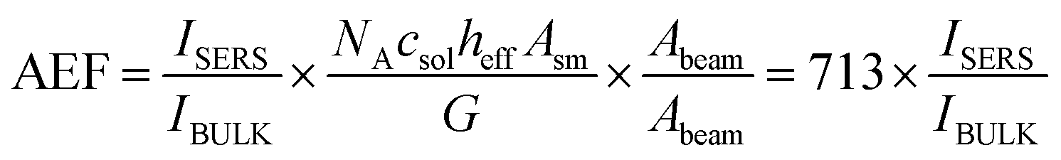
| AEF = (ISERS/NSERS)/(IBULK/NBULK) | (2) |
N BULK was calculated by considering the interaction volume of the excitation laser source and the solution concentration, csol, through:
| NBULK = NA × csol × Abeam × heff | (3) |
 | (4) |
In a real measurement setup, this translates to recording SERS spectra at discrete positions around the location where the optical focal point coincides with the substrate and calculating the total intensity of a known Raman peak over a fixed interval. In this case, measurements were conducted on a flat single crystalline silicon surface (001) in the 495 < k < 545 cm−1 band. Spectra were recorded moving with steps of 0.5 μm within a maximum range of ±5 μm close and perpendicular to the substrate, so that
 | (5) |
To determine NSERS, one needs to find the surface density of MB molecules. Hence, we consider a monolayer coverage for this analysis. The surface density is found by considering the surface area per MB molecule, Asm. We have found different values across the literature. Narband et al.68 estimated Asm based on space-filling, covalent radius, or van der Waals radius to be, 1.01 nm2, 0.66 nm2, or 3.75 nm2, respectively.68 Hang et al.69 found an Asm of 1.3 nm2 and dimensions 17.0 × 7.6 × 3.25 Å based on various sources.69 Song et al.70 conducted STM measurements on Au (111) surfaces and found an Asm of 3.5 nm2 (2.5 × 1.4 nm2 unit cell).70 The choice was made to accept the value measured by Song et al.70 as it is the only direct measurement delivering an image of the MB morphology on Au. Finally, to calculate NSERS, the surface density of molecules adhered to the surface, Asm−1, is multiplied with the total surface area:
 | (6) |
 | (7) |
3. Results and discussions
3.1 Fabrication of Au hollow nanopillars by sputter redeposition on a hybrid mask
 | ||
| Fig. 1 Schematic representation of the nanofabrication steps for the production of the Au-HNP array. (a) MEMpax® substrate. (b) sputter deposition of different Ti thicknesses (13, 20, or 40 nm). (c) Sputter deposition of 80 nm of Au. (d) Spin coating of BARC. (e) Spin coating of PFI. (f) DTL patterning over BARC. (g) Nanopillar formation with RIE of BARC. (h) Side-wall deposition of Au over the nanopillars during angled IBE-cycles. (i) Au coated nanopillar, with a zoom-in cross-section. (j) Au-HNPs after BARC removal, with zoom-in cross-section. | ||
The SHL step is then introduced for substrate fabrication. The hybrid step is conducted between steps (e) and (f) in Fig. 1 and schematically presented in Fig. 2(a) and (b). It consists of a tertiary exposure of the resist in an I-line UV source under a conventional chrome photomask (Fig. 2(b)) before development. The advantage of using the SHL is the fast and selective patterning over several μm2 to a full wafer scale within a few seconds of exposure (ca. 6 s). The pattern's final shape and size are limited by the chrome photomask resolution and the exposure wavelength.
 | ||
| Fig. 2 The left (a)–(d) scheme illustrates part of the process flow by a schematic representation of the top- and cross-section view after the sequential application of the fabrication steps. (a) DTL of PFI; (b) tertiary exposure under a conventional photomask; (c) post-bake and development of PFI; (d) directional RIE of BARC in N2 plasma. A legend is added relating the colors used in the schematics to the corresponding materials. SEM images on the right contain two micrographs of the substrate, after step (d). (e) and (f) images show the transition between the (un)masked area resulting from the tertiary exposure and RIE of BARC. (e) displays an image of the cross-section containing the BARC hybrid mask columns and (f) a top-view. The scale bars represent 2 μm. | ||
Next, reactive ion etching (RIE) in N2 plasma is used to pattern the BARC layer, partially exposing the Au surface (Fig. 1(g) and (2d)). Scanning electron microscopy (SEM) images of the BARC columns collected after transferring the hybrid resist pattern into the BARC layer are presented in Fig. 2(e)–(f). The SEM cross-section and top-view were recorded at the edge of the SHL nanopattern (see red arrow). Note that the nanodot pattern needs approximately 5 periods to become uniform. Thus, a trade-off exists between the rapidness and pattern-ability versus the edge effects observed while employing SHL (Fig. 2).
 | ||
| Fig. 3 (a) Au-HNPs with BARC and (b) Au-HNPs without BARC. Each SEM image is accompanied by a schematic representation of the nanofabricated Au structures. The scale bar is 100 nm. | ||
After Au sputter-redeposition over the BARC-nanopillars, the last step is to remove the remaining BARC inside the Au-HNP. The removal of the BARC layer is carried out by applying an oxygen (O2) plasma. Characterization of the plasma treatment is performed in a plasma asher and an RIE setup. For increased applied powers and prolonged-time, removing the BARC negatively affects the structural integrity of the Au-HNP, as can be seen in Fig. S2.† The prolonged exposure to the high power plasma introduces a high surface temperature and sintering effect, as observed by the polycrystalline domains reforming into larger grains. An optimum time for O2 plasma etching is found to be 8 min at 25 W. This step delivers an array of Au-HNPs with structural integrity, as shown in Fig. 3(b) and S3.† Images of wafer-scale fabricated substrates with and without BARC are presented in Fig. S4.†
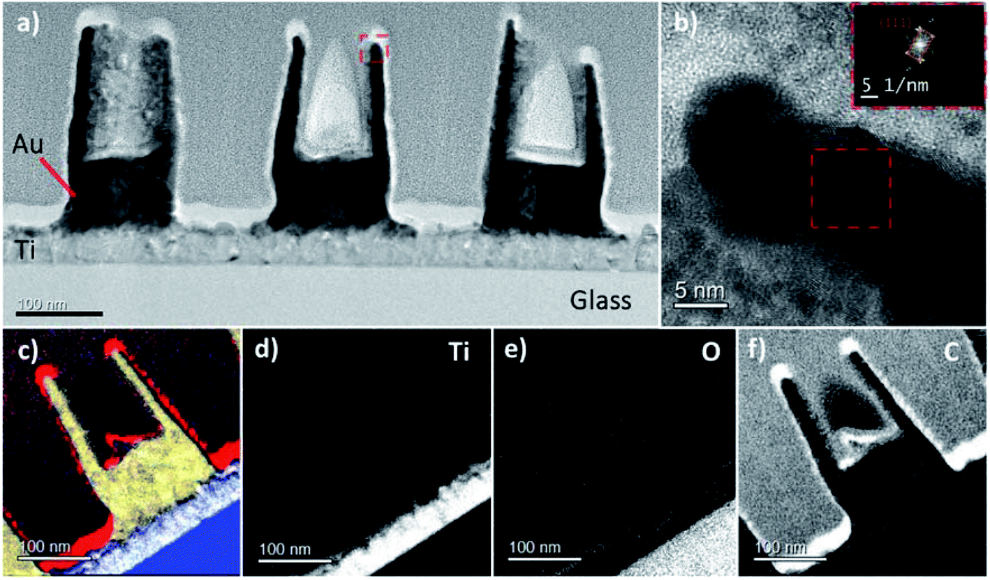 | ||
| Fig. 4 (a) TEM image of as-fabricated Au-HNPs. Scale bar reads 100 nm. (b) Close-up to one of the top edges of the Au-HNPs. The scale bar represents 5 nm. The dashed box indicates the location of the processed FFT inset. The inset scale bar represents 5 nm−1. (c) Color image representation overlaying the elemental profiles, extracted from the EF-TEM analysis, displayed in (d)–(f). In (c), red indicates carbon, blue oxygen, white titanium, and yellow indicate gold. Energy-filtered TEM image for (d) titanium, (e) oxygen, and (f) carbon. (c)–(f) scale bars represent 100 nm. | ||
Chemical composition from the energy-filtered TEM in Fig. 4(c)–(f) indicates carbon (C) in red, oxygen (O) in blue, titanium (Ti) in white, and Au in yellow. Brighter white/grey color contrast reveals the presence of C. This is expected as the C is evaporated during sample preparation for TEM. Dimer white/grey color contrast is also found for Ti and O over the Au-HNP, suggesting a thin oxidized titanium layer, possibly of TiO2. The presence of Ti is due to the exposure of the adhesion layer to Ar+ during IBE. The O layer possibly forms throughout air exposure or BARC removal from the Au-HNPs.
The Au-HNP structure is subdivided into a solid base structure with the same thickness as that of the initially sputter-deposited 80 ± 2 nm Au layer and a 170 ± 10 nm high nano-rim structure. In Fig. 3(a) and (b), the total Au-HNP height, base plus nano-rim, is ∼250 ± 12 nm, with a thin rim at the top. The outer base diameter was measured using top-view HR-SEM images with results shown in Fig. S5 and S6.† The particle dispersion based on the outer base dimension is 133 ± 4 nm. Note that the values were measured from different substrates and thus yielded batch-to-batch and location-to-location variation. Measurements of the inner nano-rim diameter conducted with TEM, shown in Fig. 4, reveal that the top of the Au-HNPs has a thin nano-rim of ca. 14 nm ± 3 nm. A schematic illustration containing all the Au-HNP dimensions extracted from the TEM images is displayed in Fig. S7.† It is worth noting that previous studies have already shown that ion beam redeposition on a photoresist mask can be used for patterning purposes. However, this work facilitates periodic organization with lattice constants small enough to be relevant for nanoplasmonics, which is different from that in Desbiolles et al.51 Furthermore, we achieved patterning of sidewall structure with resolutions of ±3 nm. In this respect, Jeon et al.50 achieved similar 3D architectures with NIL, but in our case, we have pattern-ability by SHL and show the wafer-scale homogeneity. Lastly, Mehrvar et al.75 showed the complexity of using a capacitively coupled RIE for sidewall redeposition. Utilizing an IBE gives a more controllable platform for sidewall redeposition. The DTL/SHL and angled IBE combination is necessary for device integration with well-defined plasmonic nanostructures, paving the way for complex device integration at the wafer scale.
3.2 Optical properties of the Au-HNP array
FDTD simulations for 3D Au-HNPs are performed to understand the optical response of the fabricated plasmonic array. The Au-HNP dimensions used in the numerical simulations are extracted from SEM and TEM images, summarized in Fig. S7.† First, the absorption cross-section of an isolated Au-HNP is calculated for two different cases, with and without BARC. It is noteworthy that BARC is located at the cavity of the Au-HNP (Fig. 3). Two peaks are observed in the absorption cross-section, as shown in Fig. 5(a) and (b). A charge distribution analysis is carried out to identify the supported modes of the Au-HNP at the peak wavelengths. The peak at longer wavelengths, i.e., ∼730 nm for Au-HNP with BARC and ∼650 nm for Au-HNP without BARC, corresponds to the electric-dipole resonance formed by the horizontal charge separation at the rim of the Au-HNP (right inset in Fig. 5(a) and (b)). This type of resonance has been observed in planar U-shaped plasmonic particles, like the well-known split-ring resonator geometry.78 Furthermore, the absorbance peaks in the wavelength range of 500–600 nm in Fig. 5(a) and (b) are associated with the electric-quadrupolar resonance formed by the out-of-phase vertical charge separation along the sidewalls of the Au-HNP (left inset in Fig. 5(a) and (b)). | ||
| Fig. 5 Numerically calculated absorption cross-section for a single Au-HNP (a) with and (b) without BARC for Ti thicknesses of 13, 20, and 40 nm. The insets illustrate a schematic representation of the charge distribution of the supported modes. Numerically calculated absorption spectra of arrayed Au-HNPs (c) with and (d) without BARC for Ti thicknesses of 13, 20, and 40 nm. Measured UV-VIS-NIR-absorptance spectra of arrayed Au-HNPs (e) with and (f) without BARC for Ti thicknesses of 13, 20, and 40 nm. | ||
Next, a two-dimensional square array of Au-HNPs with a 250 nm pitch was investigated. The absorptance spectra of the periodic samples with and without BARC are depicted in Fig. 5(c) and (d), for Ti layer thicknesses of 13, 20, and 40 nm. The two peaks in the absorptance spectra coincide with the assigned dipolar and quadrupolar resonances of a single Au-HNP. It is worth noting that the peak absorptance increases with an increasing Ti layer thickness, especially for Au-HNPs with BARC. This is attributed to the larger reflection from the substrate in the samples with thicker Ti layers, consequently coupling more power to the modes.79
The measured UV-VIS-NIR-absorptance spectra of Au-HNPs with and without BARC for the different Ti thicknesses are presented in Fig. 5(e) and (f). The results show that the peaks are broadened and redshifted by Δλ ∼ 90 nm if the nano-rim is filled with BARC. The resonance broadening of the dipole peak is attributed to increased optical losses and resonance inhomogeneity, likely caused by surface roughness and small variations in shape and dimension among the structures. The influence of these imperfections is not included in the simulations. It is worth mentioning that for single-crystalline Au-HNPs, narrower absorptance peaks are expected.80
It is well known that the resonance wavelengths of plasmonic particles are strongly dependent on their geometrical parameters. Thus, the effect of variations in the structural dimensions on the absorptance spectra is studied by employing FDTD simulations and factorial design analysis to understand the peak redshift observed in Fig. 5(e) and (f). The details can be found in the ESI file, Section 2.† The results of this study revealed that the thickness of the Au sidewall/nano-rim plays the dominant role in the redshift of the dipolar peak in comparison to the effects of other geometrical parameters, as shown in Fig. S11 and S12.† This is attributed to the increased length-to-width ratio of the sidewalls, which is a parameter known to affect significantly the resonance conditions of plasmonic nanostructures.81,82
The absorptance spectra of an array of Au-HNPs without BARC are calculated for different sidewall thicknesses, while other parameters remained constant to gain further insights into the redshift found for the electric dipole peak. The results in Fig. 6(a) and (b) show the dipole peak redshift as the sidewall thickness reduces, indicating a nonlinear dependency between the two quantities. It is also worth noting that small variations of ±3 nm in the wall thickness (ca. 14 nm) result in a considerably large redshift of Δλ ∼ 90 nm. Therefore, the sidewall thickness variations are primarily responsible for the redshift of the dipole peak in the experimental results, as depicted in Fig. 5(e) and (f). In addition, this variation because of the sidewall thickness is much larger than that due to variations in the thickness of the titanium adhesion layer or other geometrical aspects, as discussed in the ESI file Section 2.† Note that sidewall thicknesses > 20 nm will show no significant dipole peak contributions because of the dampened plasmonic response. As shown in Fig. 6(b), the relative shift in resonance wavelength reduces with the increasing sidewall thickness. Therefore, a thicker sidewall is expected to give more uniformity in the optical response because of the lower sensitivity to the sidewall thickness variations. However, despite fabrication challenges, a thinner sidewall is more appealing because of the increased absorption peak and the possibility of the spectral tunning of the peaks. This underlines the need for a controlled sidewall deposition, as presented in this paper.
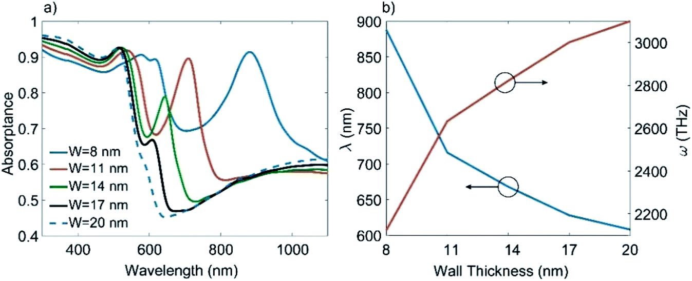 | ||
| Fig. 6 (a) Absorptance spectra of an array of Au-HNPs without BARC for different sidewall thicknesses (W), while all other structural parameters are constant. (b) The dipole peak wavelength/frequency versus sidewall thickness. | ||
3.3 Field enhancement in the Au-HNP array
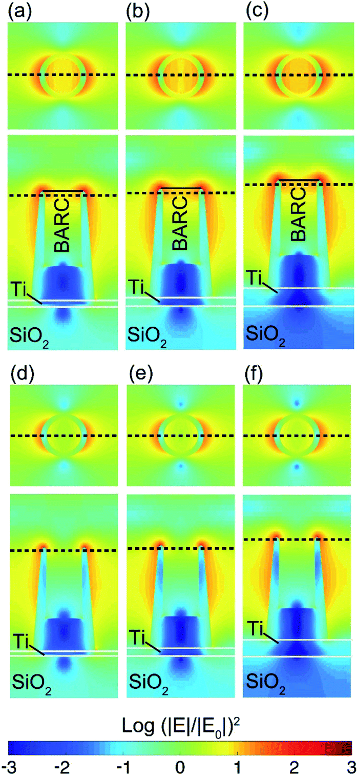
Since the numerical and experimental results show surface plasmon resonance peaks in the absorptance spectra, it is interesting to investigate the field enhancement effect over the Au-HNPs. The intensity enhancement is calculated by (|E|/|E0|)2, in which E is the spatially dependent electric field, and |E0| is the electric field amplitude of the input source. The intensity enhancement in periodic samples at their corresponding dipolar resonances at λ = 600 and 680 nm for the Au-HNPs with and without BARC is shown in Fig. 7. Here, a relatively large intensity enhancement at the rim of the Au-HNPs is found. Consequently, the EF, which is proportional to (|E|/|E0|)4, is also large in these samples. An EF as large as ∼2 × 10⁵ at 680 nm is obtained for the sample with BARC and a Ti thickness of 40 nm. This is twice as large as that for samples with thinner Ti, for example, 13 nm thick. The EF for all samples without BARC is ∼4 × 10⁴ at ∼600 nm, and it is not affected by the variation of the Ti layer thickness. For the excitation wavelength of 785 nm, which is the option of choice mainly when dealing with biological specimens, the intensity enhancement of the samples with and without BARC is shown in Fig. 8. Although the dipole absorption peaks are far from 785 nm, a comparatively large EF of the order of 104 is numerically achieved for all the samples. Higher EFs could be obtained for samples with engineered geometries, e.g., the addition of a silica shell83 in which the dipole mode spectral region is shifted toward 785 nm. | ||
| Fig. 7 Intensity enhancement (|E|/|E0|)2 for the samples with BARC and various Ti thicknesses of (a) 13, (b) 20, and (c) 40 nm at 680 nm. (|E|/|E0|)2 for the samples without BARC and various Ti thicknesses of (d). 13, (e) 20, and (f) 40 nm at 600 nm. The nanopillar size in the computational scheme is adopted from TEM images of real structures depicted in Fig. 4. A summary of the structural dimensions is shown in Fig. S7.† | ||
 | ||
| Fig. 8 Intensity enhancement (|E|/|E0|)2 for the samples with BARC and various Ti thicknesses of (a) 13, (b) 20, and (c) 40 nm at 785 nm. (|E|/|E0|)2 for the samples without BARC and various Ti thicknesses of (d). 13, (e) 20, and (f) 40 nm at 785 nm. The nanopillar size in the computational scheme is adopted from TEM images of real structures depicted in Fig. 4. A summary of the structural dimensions is shown in Fig. S7.† | ||
Fig. 9 shows the results for the conducted experiments using λex of 633 and 785 nm. Peak assignment for MB is defined in Tables S3 and S4† for both λex's, and for the following MB Raman bands: 445, 1395, and 1618 cm−1 for λ = 633 nm, and 438, 1386, and 1629 cm−1 for λ = 785 nm. The Raman bands around 438 and 445 cm−1 are assigned to C–N–C skeletal deformation.86,88 The bands at 1386 and 1395 cm−1 are attributed to C–H in-plane ring deformation, and the bands at 1618 and 1629 cm−1 are designated to C–C ring stretching. The spectra collected on the bulk methylene blue powder, as presented in Table S3,† show none of the peak-splitting (doublets) and have much fewer peaks than the spectra recorded over the Au-HNP substrate, as presented in Fig. 9. For the AEF calculations, it is assumed to yield acceptable AEF values if solely the peaks measured on the bulk powder were compared to those also measured on the Au-HNPs. Considering peaks not present in the bulk powder but present over the Au-HNP would lead to spuriously large AEF. The steps taken to derive the AEF values are described in Section 2.6. It should be noted that for Au-HNPs not functionalized with MB, no Raman signal is observed. Furthermore, no Raman signal is found for bulk BARC and Au-HNPs with BARC and absence of MB even when using the highest laser power of 5 mW.
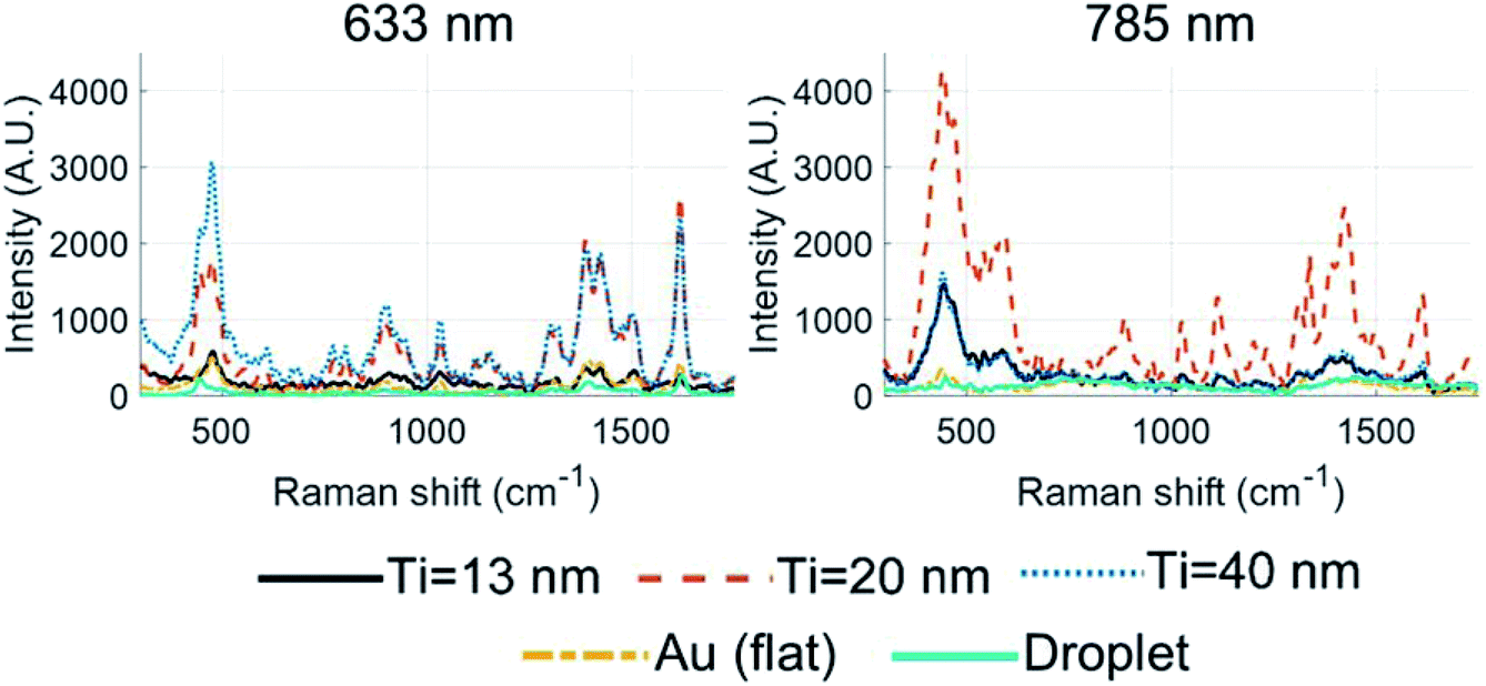 | ||
| Fig. 9 Measured Raman spectra for Au-HNPs with various Ti thicknesses (13, 20, and 40 nm) and Au (flat). Raman spectrum for a deposited droplet of MB over Au-HNPs (Ti = 20 nm) is included. MB concentration utilized for these experiments is 1 mM. | ||
For the Raman bands in Table 1, an overall enhancement factor of 103 < AEF < 104 is calculated in the case of the 633 nm excitation wavelength, which is slightly lower than predicted by the simulations. For the 13 nm substrate, the AEF is considered low, especially since the relative surface increase between the flat and structured unit cell is ∼4.79, which means an increase in AEF compared to the flat surface may be entirely due to the increase in surface area. However, assuming at least a full monolayer coverage across the entire Au-HNP surface implies an averaged AEF acting on all molecules adhered to the surface.89 Considering Fig. 7 and 8, it might well be that the SERS signal is generated only by MB molecules residing near the nano-rim, and the current calculation leads to an underestimation of the true enhancement factor. In the AEF calculations, the nano-rim area was ∼1.2% of the total surface area.
| Droplet | Ti = 13 nm | Ti = 20 nm | Ti = 40 nm | Au (flat) | ||||
|---|---|---|---|---|---|---|---|---|
| RB | RB | AEF | RB | AEF | RB | AEF | RB | AEF |
| λ = 633 nm | ||||||||
| 445 | 440 | 0.5 | 446 | 3.1 | 447 | 5.2 | 447 | 0.2 |
| 1395 | 1387 | 1.0 | 1387 | 7.1 | 1390 | 9.9 | 1393 | 0.8 |
| 1623 | 1618 | 1.3 | 1618 | 8.6 | 1619 | 8.1 | 1618 | 0.3 |
|
||||||||
| λ = 785 nm | ||||||||
| 438 | 444 | 10.8 | 440 | 48.4 | 438 | 22.4 | 438 | 1.1 |
| 1386 | 1390 | 2.5 | 1391 | 14.6 | 1390 | 4.4 | 1386 | 0.3 |
| 1629 | 1615 | 1.3 | 1609 | 36.7 | 1630 | 0.3 | 1630 | 0.2 |
Au-HNPs with 20 and 40 nm of Ti have increased performance in the case of λex 633 nm. These substrates reveal an AEF larger than that which can be contributed to the Au-HNP relative surface area alone. The effect is attributed to the Ti layer thickness, which results in a more considerable reflection and a more efficient coupling to the plasmonic resonance of the Au-HNPs, enhancing SERS. Table 1 also contains the calculated values for AEF, 103 < AEF < 105, in the 785 nm excitation wavelength. The calculated AEFs are larger for the 785 compared to the 633 nm excitation wavelength. Again, considering Fig. 7 and 8, the field intensity distribution yields a higher average value (i.e., higher probed area) when evaluated along the sidewall edges for the wavelength of 785 nm. Such an effect can be responsible for the highest detected AEF using excitation at 785 nm.
Usually, the AEF calculation and reporting are done to compare the SERS properties of different SERS substrates. In that sense, the Au-HNP is best compared to other periodic Au arrays with MB functionalization. AEFs as high as 107 are found in the case of Au nanodisks functionalized with thiophenol.90 Periodic Au nanogaps functionalized with benzenethiol lead to an AEF of 106.91 In the case of functionalized nanoparticles and nanocuboids, a 105 AEF on rhodamine 6G with a 10−8 M detection limit has been found.92 For nanocuboids, only the corners of the cuboid were considered for calculating the AEF. The AEF of 103 to 104 reported in this work is found by considering the whole area of the Au-HNPs. Chowdhury et al. stated a limit of detection of 10−10 M for MB functionalization with an AEF ∼105. However, this system consists of Au nanoprisms immobilized on PS beads and is thus very different from the well-defined Au-HNP array.93 If only the regions of high electric field intensity were considered (the nano-rim of the Au-HNPs) the AEF in our work increases by a factor of 102. Finally, to the best of our knowledge, the results indicate that the Au-HNP substrates have SERS properties and perform similarly to other reported structures.90–93
Regarding the Au-HNP array, the measured AEF can be further increased by optimizing the structural dimensions or periodicity. The FDTD model can facilitate the rational design of Au-HNPs to improve SERS characteristics. For example, the sidewall thickness can be used to tune the absorptance peak location of the Au-HNP to the excitation wavelength which can be done by altering the exposure time during the sputter deposition and/or IBE redeposition. Furthermore, a combination of the shrinkage etching of BARC with sidewall redeposition can tune the diameter of the Au-HNPs. Moreover, a phase-shift mask with different periodicities or another lithographic technique like EBL can further tailor the spatial organization and periodicity of the Au-HNP array. In the future, we aim to fabricate Au-HNPs for both nanoplasmonic sensing and spectroscopy using the versatility offered by the pattern-ability of the hybrid lithography in combination with the sputter redeposition technique.
Conclusions
SHL was used to enhance and control the pattern-ability of a DTL-derived photoresist pattern. The combination of DTL/SHL with a sputter redeposition technique confines the periodic Au-HNPs, which are arranged in a square lattice with 250 nm pitch, to specific μm2 to cm2 sized areas over the wafer, paving the way for future complex device integration. The structures consisted of an 80 ± 2 nm thick solid base with a 170 ± 10 nm tall nano-rim structure on top. By performing sputter-redeposition at an oblique angle, control over the sidewall thickness was gained, and 14 ± 3 nm thick sidewalls were obtained. FDTD simulations demonstrate that the optical response in the visible and near-infrared spectrum was dominated by plasmonic resonances (quadrupole and dipole). We have combined a factorial design with FDTD simulations to underpin the redshift of the electric dipole peak. The results reveal that a ±3 nm variation in the Au-HNP nano-rim thickness affects the surface plasmon resonance frequencies leading to a significant redshift up to ∼90 nm. This design aspect showed to be much more important than other aspects, such as the thickness of the Ti adhesion layer. These observations highlight the importance of control over the dimensions enabled by this fabrication method. Furthermore, we have demonstrated the potential of the fabricated Au-HNPs for SERS by employing MB as a probe analyte. We estimate the AEF to be ca. 103 < AEF < 104 and ca. 103 < AEF < 105 for λex of 633 and 785 nm. The AEF can be further increased by optimizing the geometry of Au-HNPs for the best SERS response. The fact that the numerical and experimental results agree well discloses the FDTD simulation potential for optimization of the optical response. We expect that Au-HNPs will find application in the fields of nanoplasmonic sensing and spectroscopy.Conflicts of interest
There are no conflicts of interest to declare.Acknowledgements
The authors would like to thank Henk Van Wolferen, Mark Smithers, and Rico Keim for their assistance during specimen preparation and SEM, and TEM image collection. Prof. Monica Morales Masis and Dr Yuri Smirnov are acknowledged for laboratory access and help during UV-VIS-NIR-experiments. Dr Hai Le-The is acknowledged for fruitful discussions. D. J. and H. G. thank the Netherlands Center for Multiscale Catalytic Energy Conversion (MCEC), an NWO Gravitation program, funded by the Ministry of Education, Culture and Science of the government of the Netherlands. I. D. L. and Z. J. acknowledge the financial support from CONACyT Grant No. CN-17-109 and the Federico Baur Endowed Chair in Nanotechnology. Part of the research leading to the results in this contribution has received funding from the European Research Council (ERC) under the European Union's Horizon 2020 research and innovation program (Grant agreement No. 742004).References
- W. L. Barnes, A. Dereux and T. W. Ebbesen, Nature, 2003, 424, 824–830 CrossRef CAS PubMed.
- C. Ciracì, R. T. Hill, J. J. Mock, Y. Urzhumov, A. I. Fernández-Domínguez, S. A. Maier, J. B. Pendry, A. Chilkoti and D. R. Smith, Science, 2012, 337, 1072–1074 CrossRef PubMed.
- C. D'Andrea, J. Bochterle, A. Toma, C. Huck, F. Neubrech, E. Messina, B. Fazio, O. M. Maragò, E. Di Fabrizio, M. Lamy De La Chapelle, P. G. Gucciardi and A. Pucci, ACS Nano, 2013, 7, 3522–3531 CrossRef.
- Z. Wang, B. Ai, Z. Zhou, Y. Guan, H. Möhwald and G. Zhang, ACS Nano, 2018, 12, 10914–10923 CrossRef CAS PubMed.
- F. De Angelis, M. Malerba, M. Patrini, E. Miele, G. Das, A. Toma, R. P. Zaccaria and E. Di Fabrizio, Nano Lett., 2013, 13, 3553–3558 CrossRef CAS.
- R. Proietti Zaccaria, F. Bisio, G. Das, G. Maidecchi, M. Caminale, C. D. Vu, F. De Angelis, E. Di Fabrizio, A. Toma and M. Canepa, ACS Appl. Mater. Interfaces, 2016, 8, 8024–8031 CrossRef CAS PubMed.
- F. Neubrech, D. Weber, J. Katzmann, C. Huck, A. Toma, E. Di Fabrizio, A. Pucci and T. Härtling, ACS Nano, 2012, 6, 7326–7332 CrossRef CAS PubMed.
- J. A. Jackman, A. Rahim Ferhan and N. J. Cho, Chem. Soc. Rev., 2017, 46, 3615–3660 RSC.
- J. Ma, X. Wang, J. Feng, C. Huang and Z. Fan, Small, 2021, 17, 1–24 Search PubMed.
- F. A. A. Nugroho, I. Darmadi, L. Cusinato, A. Susarrey-Arce, H. Schreuders, L. J. Bannenberg, A. B. da Silva Fanta, S. Kadkhodazadeh, J. B. Wagner, T. J. Antosiewicz, A. Hellman, V. P. Zhdanov, B. Dam and C. Langhammer, Nat. Mater., 2019, 18, 489–495 CrossRef CAS PubMed.
- X. Wang, S.-C. Huang, S. Hu, S. Yan and B. Ren, Nat. Rev. Phys., 2020, 2, 253–271 CrossRef.
- B. Yan, A. Thubagere, W. R. Premasiri, L. D. Ziegler, L. D. Negro and B. M. Reinhard, ACS Nano, 2009, 3, 1190–1202 CrossRef CAS PubMed.
- A. Chauvin, M. Lafuente, J. Y. Mevellec, R. Mallada, B. Humbert, M. P. Pina, P. Y. Tessier and A. El Mel, Nanoscale, 2020, 12, 12602–12612 RSC.
- H. K. Lee, Y. H. Lee, C. S. L. Koh, G. C. Phan-Quang, X. Han, C. L. Lay, H. Y. F. Sim, Y. C. Kao, Q. An and X. Y. Ling, Chem. Soc. Rev., 2019, 48, 731–756 RSC.
- H. Wei and H. Xu, Nanoscale, 2013, 5, 10794–10805 RSC.
- M. Lafuente, I. Pellejero, V. Sebastián, M. A. Urbiztondo, R. Mallada, M. P. Pina and J. Santamaría, Sens. Actuators, B, 2018, 267, 457–466 CrossRef CAS.
- J. Henzie, S. C. Andrews, X. Y. Ling, Z. Li and P. Yang, Proc. Natl. Acad. Sci. U. S. A., 2013, 110, 6640–6645 CrossRef CAS PubMed.
- Y. Yang, Y. H. Lee, I. Y. Phang, R. Jiang, H. Y. F. Sim, J. Wang and X. Y. Ling, Nano Lett., 2016, 16, 3872–3878 CrossRef CAS.
- Y. H. Lee, W. Shi, H. K. Lee, R. Jiang, I. Y. Phang, Y. Cui, L. Isa, Y. Yang, J. Wang, S. Li and X. Y. Ling, Nat. Commun., 2015, 6, 1–7 Search PubMed.
- M. Lafuente, I. Pellejero, A. Clemente, M. A. Urbiztondo, R. Mallada, S. Reinoso, M. P. Pina and L. M. Gandía, ACS Appl. Mater. Interfaces, 2020, 12, 36458–36467 CrossRef CAS PubMed.
- Q. Zhang, Y. H. Lee, I. Y. Phang, C. K. Lee and X. Y. Ling, Small, 2014, 10, 2703–2711 CrossRef CAS PubMed.
- T. Udayabhaskararao, T. Altantzis, L. Houben, M. Coronado-Puchau, J. Langer, R. Popovitz-Biro, L. M. Liz-Marzán, L. Vukovic, P. Král, S. Bals and R. Klajn, Science, 2017, 358, 514–518 CrossRef CAS.
- A. Shiohara, Y. Wang and L. M. Liz-Marzán, J. Photochem. Photobiol., C, 2014, 21, 2–25 CrossRef CAS.
- M. Fan, G. F. S. Andrade and A. G. Brolo, Anal. Chim. Acta, 2011, 693, 7–25 CrossRef CAS PubMed.
- D. E. Johnston, D. R. Strachan and A. T. C. Johnson, Nano Lett., 2007, 7, 2774–2777 CrossRef CAS PubMed.
- G. Yin, S. Bai, X. Tu, Z. Li, Y. Zhang, W. Wang, J. Lu and D. He, Nanoscale Res. Lett., 2019, 14, 168 CrossRef.
- Q. Guo, M. Xu, Y. Yuan, R. Gu and J. Yao, Langmuir, 2016, 32, 4530–4537 CrossRef CAS PubMed.
- S.-M. Yang, S. G. Jang, D.-G. Choi, S. Kim and H. K. Yu, Small, 2006, 2, 458–475 CrossRef CAS PubMed.
- M. Cottat, N. Lidgi-Guigui, I. Tijunelyte, G. Barbillon, F. Hamouda, P. Gogol, A. Aassime, J. M. Lourtioz, B. Bartenlian and M. L. de la Chapelle, Nanoscale Res. Lett., 2014, 9, 1–6 CrossRef CAS.
- K. T. Arat, T. Klimpel, A. C. Zonnevylle, W. S. M. M. Ketelaars, C. Th. H. Heerkens and C. W. Hagen, J. Vac. Sci. Technol., B: Nanotechnol. Microelectron.: Mater., Process., Meas., Phenom., 2019, 37, 051603 Search PubMed.
- C. Mack, Fundamental Principles of Optical Lithography, The Science of Microfabrication, 2007 Search PubMed.
- Q. Zou, S. Mo, X. Pei, Y. Wang, T. Xue, M. Mayilamu and G. Qin, AIP Adv., 2018, 8, 085302 CrossRef.
- N. Vogel, C. K. Weiss and K. Landfester, Soft Matter, 2012, 8, 4044–4061 RSC.
- P. A. Mosier-Boss, Nanomaterials, 2017, 7, 1–31 CrossRef PubMed.
- N. J. Greybush, I. Liberal, L. Malassis, J. M. Kikkawa, N. Engheta, C. B. Murray and C. R. Kagan, ACS Nano, 2017, 11, 2917–2927 CrossRef CAS PubMed.
- W. J. Thrift, C. Q. Nguyen, M. Darvishzadeh-Varcheie, S. Zare, N. Sharac, R. N. Sanderson, T. J. Dupper, A. I. Hochbaum, F. Capolino, M. J. Abdolhosseini Qomi and R. Ragan, ACS Nano, 2017, 11, 11317–11329 CrossRef CAS PubMed.
- S. Ni, M. J. K. Klein, N. D. Spencer and H. Wolf, Langmuir, 2014, 30, 90–95 CrossRef CAS PubMed.
- J. F. Bryche, F. Hamouda, M. Besbes, P. Gogol, J. Moreau, M. Lamy de la Chapelle, M. Canva and B. Bartenlian, Micro and Nano Engineering, 2019, 2, 122–130 CrossRef.
- M. Nayfeh, in Fundamentals and Applications of Nano Silicon in Plasmonics and Fullerines, Elsevier, 2018, vol. 135, pp. 89–137 Search PubMed.
- Y. Chen, Microelectron. Eng., 2015, 135, 57–72 CrossRef CAS.
- J. S. Hwang and M. Yang, Sensors, 2018, 18, 4076 CrossRef.
- H. H. Solak, C. Dais and F. Clube, Opt. Express, 2011, 19, 10686 CrossRef CAS PubMed.
- H. Le-The, E. Berenschot, R. M. Tiggelaar, N. R. Tas, A. van den Berg and J. C. T. Eijkel, Adv. Mater. Technol., 2016, 2, 1600238 CrossRef.
- P. Chausse, E. le Boulbar, P.-M. Coulon and P. A. Shields, Opt. Express, 2019, 27, 32037 CrossRef CAS.
- P. M. Coulon, B. Damilano, B. Alloing, P. Chausse, S. Walde, J. Enslin, R. Armstrong, S. Vézian, S. Hagedorn, T. Wernicke, J. Massies, J. Zúñiga-Pérez, M. Weyers, M. Kneissl and P. A. Shields, Microsyst. Nanoeng., 2019, 5, 52 CrossRef CAS PubMed.
- A. Susarrey-Arce, K. M. Czajkowski, I. Darmadi, S. Nilsson, I. Tanyeli, S. Alekseeva, T. J. Antosiewicz and C. Langhammer, Nanoscale, 2019, 11, 21207–21217 RSC.
- B. Gerislioglu, L. Dong, A. Ahmadivand, H. Hu, P. Nordlander and N. J. Halas, Nano Lett., 2020, 20, 2087–2093 CrossRef CAS PubMed.
- Z. Zhang, T. Deckert-Gaudig, P. Singh and V. Deckert, Chem. Commun., 2015, 51, 3069–3072 RSC.
- L. V. Brown, H. Sobhani, J. B. Lassiter, P. Nordlander and N. J. Halas, in ACS Nano, American Chemical Society, 2010, vol. 4, pp. 819–832 Search PubMed.
- M. Dipalo, H. Amin, L. Lovato, F. Moia, V. Caprettini, G. C. Messina, F. Tantussi, L. Berdondini and F. De Angelis, Nano Lett., 2017, 17, 3932–3939 CrossRef CAS PubMed.
- L. P. Hackett, W. Li, A. Ameen, L. L. Goddard and G. L. Liu, J. Phys. Chem. C, 2018, 122, 6255–6266 CrossRef CAS.
- J. A. Huang, V. Caprettini, Y. Zhao, G. Melle, N. MacCaferri, L. Deleye, X. Zambrana-Puyalto, M. Ardini, F. Tantussi, M. Dipalo and F. De Angelis, Nano Lett., 2019, 19, 722–731 CrossRef PubMed.
- H. J. Jeon, H. W. Yoo, E. H. Lee, S. W. Jang, J. S. Kim, J. K. Choi and H. T. Jung, Nanoscale, 2013, 5, 2358–2363 RSC.
- B. X. E. Desbiolles, A. Bertsch and P. Renaud, Microsyst. Nanoeng., 2019, 5, 11 CrossRef CAS PubMed.
- W.-B. Jung, S. Jang, S.-Y. Cho, H.-J. Jeon and H.-T. Jung, Adv. Mater., 2020, 1907101 CrossRef CAS PubMed.
- L. V. Jenni, L. Kumar and C. Hierold, Microelectron. Eng., 2019, 209, 10–15 CrossRef CAS.
- S. Steen, S. J. McNab, L. Sekaric, I. Babich, J. Patel, J. Bucchignano, M. Rooks, D. M. Fried, A. W. Topol, J. R. Brancaccio, R. Yu, J. M. Hergenrother, J. P. Doyle, R. Nunes, R. G. Viswanathan, S. Purushothaman and M. B. Rothwell, Microelectron. Eng., 2006, 83, 754–761 CrossRef CAS.
- A. Star, T.-R. Han, V. Joshi, J.-C. P. Gabriel and G. Grüner, Adv. Mater., 2004, 16, 2049–2052 CrossRef CAS.
- A. F. Chrimes, K. Khoshmanesh, P. R. Stoddart, A. Mitchell and K. Kalantar-Zadeh, Chem. Soc. Rev., 2013, 42, 5880–5906 RSC.
- M. R. Willner, K. S. McMillan, D. Graham, P. J. Vikesland and M. Zagnoni, Anal. Chem., 2018, 90, 12004–12010 CrossRef CAS PubMed.
- M. R. Bailey, A. M. Pentecost, A. Selimovic, R. S. Martin and Z. D. Schultz, Anal. Chem., 2015, 87, 4347–4355 CrossRef CAS PubMed.
- H. Le-The, J. J. A. Lozeman, M. Lafuente, P. Muñoz, J. G. Bomer, H. Duy-Tong, E. Berenschot, A. Van Den Berg, N. R. Tas, M. Odijk and J. C. T. Eijkel, Nanoscale, 2019, 11, 12152–12160 RSC.
- Q. Zhou and T. Kim, Sens. Actuators, B, 2016, 227, 504–514 CrossRef CAS.
- H. J. Jeon, K. H. Kim, Y. K. Baek, D. W. Kim and H. T. Jung, Nano Lett., 2010, 10, 3604–3610 CrossRef CAS PubMed.
- P. H. C. Eilers, Anal. Chem., 2003, 75, 3631–3636 CrossRef CAS.
- T. O. Haver, A Pragmatic Introduction to Signal Processing with Applications in Scientific Measurement, CreateSpace Independent Publishing Platform, 3rd edn, 2017, pp. 1–121 Search PubMed.
- E. C. le Ru, E. Blackie, M. Meyer and P. G. Etchegoint, J. Phys. Chem. C, 2007, 111, 13794–13803 CrossRef CAS.
- N. Narband, M. Uppal, C. W. Dunnill, G. Hyett, M. Wilson and I. P. Parkin, Phys. Chem. Chem. Phys., 2009, 11, 10513–10518 RSC.
- P. T. Hang and G. W. Brindley, Clays Clay Miner., 1970, 18, 203–212 CrossRef.
- Y. Song and L. Wang, Microsc. Res. Tech., 2009, 72, 79–84 CrossRef CAS PubMed.
- P. J. Westerik, W. J. C. Vijselaar, J. W. Berenschot, N. R. Tas, J. Huskens and J. G. E. Gardeniers, J. Micromech. Microeng., 2018, 28, 015008 CrossRef.
- J. J. Cuomo, S. M. Rossnagel, H. R. Haufman and R. Komanduri, Handbook of Ion Beam Processing Technology: Principles, Deposition, Film Modification, and Synthesis, 1990, vol. 112 Search PubMed.
- H. Le-The, E. Berenschot, R. M. Tiggelaar, N. R. Tas, A. van den Berg and J. C. T. Eijkel, Microsyst. Nanoeng., 2018, 4, 1–10 CrossRef CAS PubMed.
- R. E. Lee, J. Vac. Sci. Technol., 1979, 16, 164–170 CrossRef CAS.
- L. Mehrvar, H. Hajihoseini, H. Mahmoodi, S. H. Tavassoli, M. Fathipour and S. M. Mohseni, Nanotechnology, 2017, 28, 315301 CrossRef CAS.
- F. Frost, R. Fechner, B. Ziberi, D. Flamm and A. Schindler, Thin Solid Films, 2004, 459, 100–105 CrossRef CAS.
- N. Toyoda, T. Hirota, I. Yamada, H. Yakushiji, T. Hinoue, T. Ono and H. Matsumoto, IEEE Trans. Magn., 2010, 46, 1599–1602 CAS.
- I. de Leon, M. J. Horton, S. A. Schulz, J. Upham, P. Banzer and R. W. Boyd, Sci. Rep., 2015, 5, 1–9 Search PubMed.
- Y. Guo, S. Jiang, X. Chen, M. Mattei, J. A. Dieringer, J. P. Ciraldo and R. P. van Duyne, J. Phys. Chem. C, 2018, 122, 14865–14871 CrossRef CAS.
- J. S. Huang, V. Callegari, P. Geisler, C. Brüning, J. Kern, J. C. Prangsma, X. Wu, T. Feichtner, J. Ziegler, P. Weinmann, M. Kamp, A. Forchel, P. Biagioni, U. Sennhauser and B. Hecht, Nat. Commun., 2019, 1, 150 CrossRef PubMed.
- C. Rockstuhl, F. Lederer, C. Etrich, T. Zentgraf, J. Kuhl and H. Giessen, Opt. Express, 2006, 14, 8827 CrossRef PubMed.
- G. W. Bryant, F. J. García De Abajo and J. Aizpurua, Nano Lett., 2008, 8, 631–636 CrossRef CAS PubMed.
- A. Vanderkooy, Y. Chen, F. Gonzaga and M. A. Brook, ACS Appl. Mater. Interfaces, 2011, 3, 3942–3947 CrossRef CAS PubMed.
- M. A. Bedics, H. Kearns, J. M. Cox, S. Mabbott, F. Ali, N. C. Shand, K. Faulds, J. B. Benedict, D. Graham and M. R. Detty, Chem. Sci., 2015, 6, 2302–2306 RSC.
- S. Dutta Roy, M. Ghosh and J. Chowdhury, J. Phys. Chem. C, 2018, 122, 10981–10991 CrossRef CAS.
- G. N. Xiao and S. Q. Man, Chem. Phys. Lett., 2007, 447, 305–309 CrossRef CAS.
- S. T. Sivapalan, B. M. Devetter, T. K. Yang, T. Van Dijk, M. V. Schulmerich, P. S. Carney, R. Bhargava and C. J. Murphy, ACS Nano, 2013, 7, 2099–2105 CrossRef CAS PubMed.
- S. H. Seo, B. M. Kim, A. Joe, H. W. Han, X. Chen, Z. Cheng and E. S. Jang, Biomaterials, 2014, 35, 3309–3318 CrossRef CAS PubMed.
- Y. Song and L. Wang, Microsc. Res. Tech., 2009, 72, 79–84 CrossRef CAS.
- J. F. Bryche, R. Gillibert, G. Barbillon, M. Sarkar, A. L. Coutrot, F. Hamouda, A. Aassime, J. Moreau, M. Lamy de la Chapelle, B. Bartenlian and M. Canva, J. Mater. Sci., 2015, 50, 6601–6607 CrossRef CAS.
- H. Le-The, J. J. A. Lozeman, M. Lafuente, P. Muñoz, J. G. Bomer, H. Duy-Tong, E. Berenschot, A. van den Berg, N. R. Tas, M. Odijk and J. C. T. Eijkel, Nanoscale, 2019, 11, 12152–12160 RSC.
- G. Das, M. Chirumamilla, A. Toma, A. Gopalakrishnan, R. P. Zaccaria, A. Alabastri, M. Leoncini and E. di Fabrizio, Sci. Rep., 2013, 3, 1–6 Search PubMed.
- E. Chowdhury, M. S. Rahaman, N. Sathitsuksanoh, C. A. Grapperhaus and M. G. O. Toole, Nanotechnology, 2021, 32, 025506 CrossRef CAS PubMed.
Footnotes |
| † Electronic supplementary information (ESI) available. See DOI: 10.1039/d1na00316j |
| ‡ These authors contributed equally. |
| This journal is © The Royal Society of Chemistry 2021 |