
 Open Access Article
 This Open Access Article is licensed under a Creative Commons Attribution-Non Commercial 3.0 Unported Licence
Formation of arsenic clusters in InAs nanowires with an Al2O3 shell
In Kim†
a,
Suji Choi†bc,
Ji-Hwan Kwonb,
Sang Jung Ahnb,
Min Sun Yeoma,
Ho Seong Lee c,
Seong-Hoon Yic and
Young Heon Kim*d
c,
Seong-Hoon Yic and
Young Heon Kim*d
aCenter for Supercomputing Applications, Korea Institute of Science and Technology Information, 245 Daehak-ro, Daejeon 34141, Republic of Korea
bKorea Research Institute of Standards and Science, 267 Gajeong-Ro, Yuseong-Gu, Daejeon 34113, Republic of Korea
cKyungpook National University, 80 Daehak-ro, Buk-gu, Daegu 41566, Republic of Korea
dGraduate School of Analytical Science and Technology (GRAST), Chungnam National University, 99 Daehak-ro, Yuseong-gu, Daejeon 34134, Republic of Korea. E-mail: y.h.kim@cnu.ac.kr
First published on 22nd December 2020
Abstract
An in-depth understanding of thermal behavior and phase evolution is required to apply heterostructured nanowires (NWs) in real devices. The intermediate status during the vaporization process of InAs NWs in an Al2O3 shell was studied by conducting quenching during in situ heating experiments, using a transmission electron microscope. The formation of As clusters in the amorphous Al2O3 shell was confirmed by analyzing the high-angle annular dark field images and energy-dispersive X-ray spectra. The As clusters existed independently in the shell and were also observed at the end of the InAs pieces obtained after quenching. The formation process of the As clusters was demonstrated from a theoretical perspective. Moreover, an ab initio molecular dynamics simulation (AIMD) was conducted to study the atomic and molecular behaviors.
Introduction
Semiconductor nanowires (NWs) of III-arsenide compounds have received attention as active components in electronic and optical nanodevices and electrical interconnections.1–3 Besides, the formation of heterostructured NWs, e.g. core–shell NWs, has been required to fabricate an ideal device and has also been suggested to improve the functionality of a NW-based device. The physical and chemical properties of heterostructured NWs are largely affected by the interface boundary effect and surface structure due to their large surface-to-volume ratio. Many researchers have attempted to understand novel phenomena of phase transition and/or transformation on the heterostructured NWs and to enhance the performance of NW-based devices by fabricating heterostructured systems.4–10 As the physical and chemical properties of pure NWs differ from those in bulk, the physical and chemical properties of heterostructured NWs also differ from those in bulk systems. To apply heterostructured NWs in real devices, an in-depth understanding of various physical and chemical properties besides thermal behavior and phase evolution is required.Thermal behavior and phase evolution in heterostructured nanomaterials have been studied recently using transmission electron microscopy (TEM).11–13 Recently well-established in situ heating TEM experiments can provide an alternative way to study the vaporization process for nanometer-sized materials by monitoring morphological and microstructural properties in real time with a high resolution of individual nanostructures. Moreover, the volumes of melting, vaporization, and condensation molecules can be quantified by considering the 3-dimensional morphology, and the exact sizes of these molecules, and the dynamic behaviors of the vaporization processes can be understood by analyzing the bright-field (BF) and high-resolution (HR) TEM images. Based on advanced TEM techniques, several studies have reported specific phase transition phenomena in nanomaterials by adopting various heterostructured nanomaterials.14–16
In this study, we report the observation of arsenic (As) clusters formed during the in situ heating TEM experiments of InAs NWs covered with an Al2O3 thin shell. Al2O3 has been widely used in shell structure engineering for producing nanotubes for drug delivery, and it has also been widely considered as a passivation layer in III-As compound semiconductors.15,16 In addition, an Al2O3 thin film imparts visibility to the phase evolution behavior of target materials during TEM imaging because of its amorphous structure. The atomistic evolution after the decomposition of indium and arsenic atoms is demonstrated by analyzing the results from molecular dynamics simulation.
Experimental
InAs NWs were grown on Si (111) substrates without metal catalysts using molecular beam epitaxy (MBE). In and As fluxes were 3 × 10⁻⁸ and 1.2 × 10⁻⁵ torr respectively, and the growth temperature of InAs NWs was 430 °C. The grown InAs NWs were separated and dispersed in an isopropyl alcohol (IPA) solution from the Si substrate by ultrasonic treatment. The IPA solution with InAs NWs was dropped onto a TEM electronic heating chip (Fusion, Protochips Inc., USA). The chip with InAs NWs was loaded into a thermal atomic layer deposition (ALD) chamber (S200, Savannah, Cambridge NanoTech Inc., USA). Al2O3 shells were deposited from the reaction of trimethylaluminum (Al(CH3)3, TMA, Sigma Aldrich, USA) with H2O at 70 °C. The flow tube pressure was ∼100 mTorr during the deposition. The detailed ALD processes for Al2O3 shells have been described elsewhere.17 After the ALD process, the grid and heating device were placed on TEM holders for microstructural characterization and in situ heating TEM experiments. The in situ TEM experiments were conducted using a field-emission gun (FEG) transmission electron microscope operating at an accelerating voltage of 300 kV (FEI Tecnai F30 S-Twin, USA). The continuous change process of InAs/Al2O3 heterostructured NWs with increasing temperature was monitored. A time series of TEM images was recorded using a Gatan charge-coupled device camera with an acquisition rate of 5 frames s−1. InAs NWs were monitored over a wide range of temperatures from 20 °C up to 800 °C with a ramping rate of 10 °C min−1 in this study. To check the intermediate status, the heating system was quenched to 20 °C when the heating temperature reached 700 °C. After the quenching process, the microstructural characterization and compositional analyses of InAs NWs were conducted by using high-angle annular dark field (HAADF) imaging and energy-dispersive X-ray spectroscopy (EDS) analysis. A field-emission gun transmission electron microscope (FEG-TEM, FEI Titan G2 ChemiSTEM 80–200 kV, USA) was used for performing HAADF imaging and EDS analysis.We performed an ab initio molecular dynamics (AIMD) simulation to observe the dynamics of the surface atoms of InAs NWs. We adopted the projector-augmented wave method implemented in the Vienna ab initio simulation package.18 The flavor of Perdew–Berke–Ernzerhof exchange correlation function was adopted with a 400 eV plane wave basis energy cut-off.19 A slab model of In-terminated InAs(100) with a thickness of 20 Å (containing 64 atoms in total) was generated with a vacuum layer along the c-axis direction. The system was simulated based on the NVT ensemble for 40 ps at 1500 K using the Nosé-Hoover thermostat with 1.0 fs timestep. A set of 4 × 4 × 1 k-point grids was employed to sample the 1st Brillouin zone. To model the slab surface during the dynamics simulation, two In and As layers were fixed to mimic bulk states. Diffusion coefficients were calculated using TRAVIS, and the radial distribution functions were analyzed using VMD.20,21
Results
Fig. 1 shows the typical morphological and microstructural evolutions of InAs NWs with Al2O3 thin shell during in situ heating TEM experiments. The Al2O3 shells were uniformly deposited on InAs NWs through the ALD process with a thickness in the range of 15 to 16 nm. The microstructural properties of InAs NWs adopted in our experiments were described in detail in our previous study.17 Based on the analyses of the selected area electron diffraction patterns and the results of the fast Fourier transform of HRTEM images, it was confirmed that the Al2O3 thin shells were amorphous. The diameter of InAs NWs was in the range of several tens to several hundreds of nanometers, and it was also confirmed that InAs NWs were fully covered by the Al2O3 shells. With increasing temperature, the disappearance of InAs NWs in the Al2O3 shells was detected, and the vacant area gradually increased (Fig. 1(b) and (c)). Specifically, the decomposition of InAs started at the interface between the InAs cores and the Al2O3 shells, and the vacant areas were occasionally formed at the corner and/or in the middle of InAs NWs. In Fig. 1(b), the small red arrows indicate the decomposition positions at the corners, whereas the large red arrows indicate the decomposition initiation in the middle parts of InAs NWs. Segmented InAs parts were formed in InAs NWs with continuing decomposition because the decomposition started simultaneously in several parts of these NWs (Fig. 1(c)). When the temperature reached above 743 °C, InAs rapidly decomposed and completely disappeared within a few seconds (Fig. 1(d)).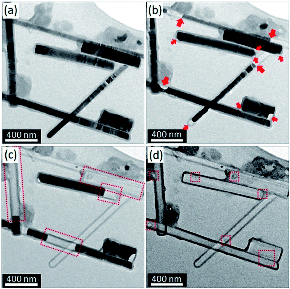 | ||
| Fig. 1 In situ TEM images during heat treatment indicating the morphological and microstructural evolutions of InAs/Al2O3 core/shell systems. (a) RT, (b) 600.0 °C, (c) 742.5 °C, and (d) 745.0 °C. | ||
Fig. 2 shows the HAADF-scanning TEM (STEM) images and the EDS results for the InAs/Al2O3 heterostructured NWs that remained localized after the completion of the in situ heating TEM experiments at 705 °C. In the HAADF-STEM image shown in Fig. 2(a), white bar-like structures appear to be present in the Al2O3 shell. However, the bar-like structure in region L1 in Fig. 2(a) is darker compared with other white bar-like structures. Moreover, it is slightly discontinuous and has non-uniform contrast. The EDS results obtained by the local elemental mapping method, which are depicted in Fig. 2(b)–(e), show the spatial distributions of the chemical elements In, As, O, and Al on the heterostructured NWs after the in situ heating TEM experiment. Region L1 was devoid of In atoms, although the other bar-like structures consisted of the chemical element In. On the other hand, the signal intensity for As atoms in region L1 was much stronger than the other areas. The EDS results indicated that region L1 was composed only of pure As atoms, whereas the other bar-like structures were composed of both In and As atoms. The signals for Al and O were intense in the shell area and almost same at the inside and outside of the shell.
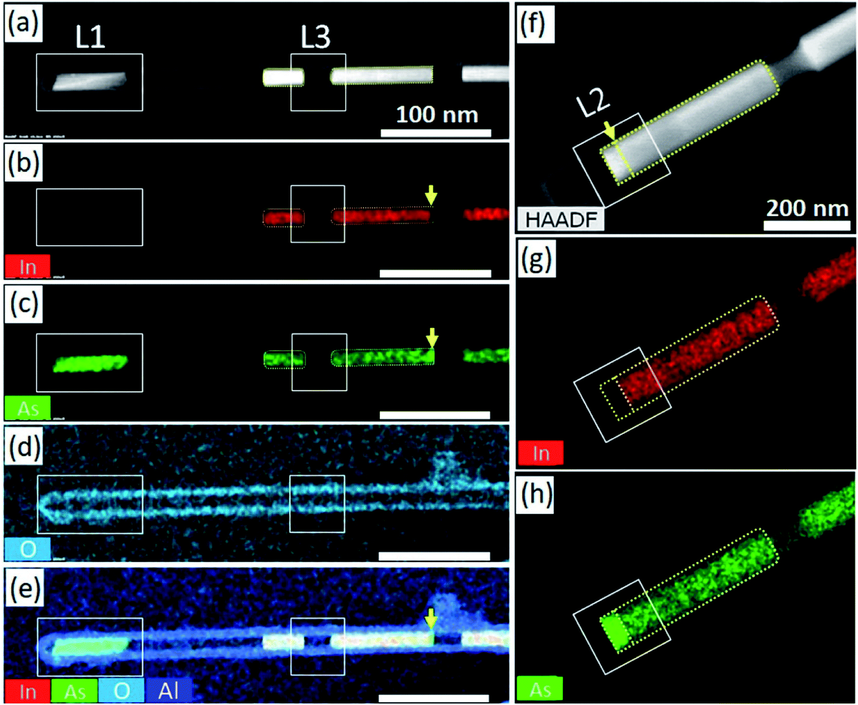 | ||
| Fig. 2 (a) HAADF-STEM image captured using the InAs/Al2O3 core/shell system. (b–d) Elemental mapping of the In (shown in red), As (green), and oxygen (sky-blue) contents of the core/shell system, respectively. (e) Overlapped elemental mapping of the In, As, O, and Al contents. (f) Magnified HAADF-STEM image obtained from the InAs/Al2O3 core/shell system. (g and h) Elemental mapping of In (shown in red) and As (green), respectively. The arrows indicate the existence of As clusters at the end of the InAs parts. | ||
Moreover, the shell area was completely devoid of In and As atoms. Therefore, we deduced that the chemical reaction between the InAs core and the Al2O3 shell did not occur during the in situ heating TEM experiment. Specifically, the strong signal intensity from As atoms was occasionally detected at the ends of the white bar-like structures, as indicated by the yellow arrows in Fig. 2(b), (c), and (e). The HAADF-STEM image in Fig. 2(f) and the EDS area mappings in Fig. 2(g) and (h) clearly show the localized As cluster at the end of the InAs core. The discontinuity of contrast was detected at the end of the InAs core, indicated by the yellow arrow in the HAADF-STEM image (Fig. 2(f)). The EDS mappings for In and As atoms clearly showed that As atoms were localized at the end of the InAs core, and the signal intensity was uniform in the area at the end of the InAs core. It is important to note that some of the vacant regions, e.g. the vacant area in region L3 in Fig. 2(a), are devoid of As clustering.
After the in situ heating process in the transmission electron microscope, HR TEM images were obtained for investigating the atomic structures. Fig. 3(a) shows the TEM image obtained from region L2 in Fig. 2(f), which was formed under the multi-beam condition. The interface between pre-existing InAs and the newly formed As cluster was abrupt, although a few thin steps with a thickness in the range of approximately two or three monolayers were observed at the interface. Even after the in situ heating TEM experiment, the thickness of the Al2O3 thin shell remained constant at 15 nm, and it was the same as that of the as-deposited film.
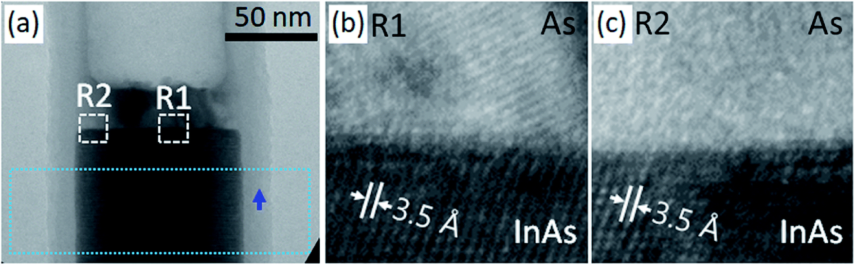 | ||
| Fig. 3 (a) BFTEM image captured at the region including the As cluster at the end of the InAs part. The line profile in (a) indicates the change in signal intensity along the dotted rectangle, and the arrow shows the discontinuity of contrast change. (b and c) HRTEM micrographs presenting the atomic structures in regions R1 and R2, respectively. | ||
However, a slight change in contrast, as indicated by the blue arrow in the BFTEM image, occurred in the Al2O3 shell (Fig. 3(a)). Fig. 3(a) shows that the variation in the contrast in the Al2O3 shell is smooth in the left side, whereas it is slightly abrupt in the right side. The variation in the contrast was detected in the As cluster. Further, the variation in contrast in a TEM image can be caused by the differences in mass, thickness, crystallinity, and orientation of crystal structures in a specimen. In the case of the As cluster, the contrast change was predominantly caused by the crystallinity. The HRTEM image (Fig. 3(b)) obtained from region R1 in Fig. 3(a), in which bright-and-dark contrast is observed, shows the crystallized atomic structure in the As cluster.
On the other hand, the HRTEM image (Fig. 3(c)) obtained from region R2 in Fig. 3(a) indicates that the As cluster area in region R2 is devoid of crystallization. The inter-planar spacing (∼3.2 Å) observed in the As cluster in Fig. 3(b) is close to that of the {101} planes of the As crystal with a rhombohedral structure. Moreover, a Moiré pattern was observed near the middle of the cluster. From these observations, we deduced that As atoms might have been partially crystallized during the rapid cooling process after the in situ heating TEM experiment.
Discussion
As clustering is a specific phenomenon. The As atoms that originated from the decomposition of InAs were condensed on the As cluster, indicating that As atoms are retained by the Al2O3 thin shell, whereas In atoms selectively escape through the Al2O3 shell. However, because the atomic and ionic radii of As atoms are smaller than those of In atoms (i.e., the atomic and electronic radii of As are 1.3 Å and 0.58 Å, respectively, and those of In are 2.0 Å and 0.8 Å, respectively), it can be deduced that the escape of As atoms through the Al2O3 thin shell is more favorable than that of In atoms.The existence of pores and/or pinholes in Al2O3 thin films deposited by the ALD method has been reported by a few research groups.22,23 The changes of atomic structures in Al2O3 deposited by ALD method might have been caused by the in situ heating experiments.24,25 Moreover, the accelerated crystallization of the amorphous Al2O3 shell by an electron beam at a low temperature (600 °C) has been reported by Huang et al.15 Therefore, we deduce that there are a few routes for the escape of atoms and/or molecules in the Al2O3 shells, probably formed during the deposition and the post in situ heating. In the actual experiment, the shape and/or morphology of the as-prepared Al2O3 thin shell gradually changed as the temperature increased; a shell shrink, a microcrack, and a small hole were finally generated at the local areas on the Al2O3 layer, indicated by the squares in Fig. 1(d). We therefore conclude that the decomposition proceeds with an increase in temperature, and the decomposed In and As atoms escape through the small paths in the thin shells.
In general, As vaporization occurs more rapidly than metal vaporization. Therefore, it causes the problem of leaving metal droplets on the surface while growing a thin film by using MBE at a high temperature.26–28
However, in our experiments, it was confirmed that a fertile region of As, not In, occurs in the Al2O3 thin shells. Our AIMD simulations show the distinct behavior of As atoms. At a highly elevated temperature of 1500 K (= 1226.85 °C), both In and As atoms rapidly fluctuate near the surface. Fig. 4(a) shows the radial distribution function (RDF) of In and As atoms near the surface plotted as a function of distance. For As atoms, the first peak followed by a local minimum is clearly shown, whereas such a peak is not observed for In atoms. The coordination number can be calculated from the integral of RDF up to the first minima, and the value of surface As atoms reads as ∼1.27.
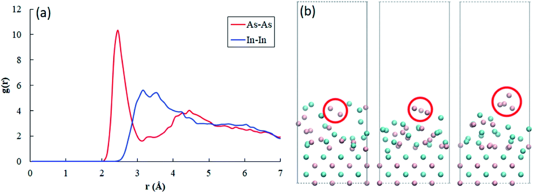 | ||
| Fig. 4 Radial distribution functions g(r) of As–As and In–In at the surface. The function of As atoms clearly shows a peak and the first local minimum indicating As–As pair, whereas In atoms do not exhibit such a behavior. (b) Evidence of existence of As2 (dimer), As3 (trimer) and As4 (tetramer) near the surface during the dynamics simulation. The red circle shows the evolution of such molecules. The atomic configurations are visualized using the VMD package.21 | ||
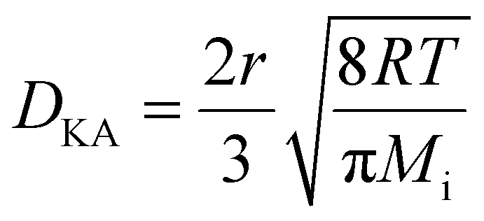
This result indicates that As atoms are more prone to form a molecule than In atoms. Indeed, we observed As dimers, trimers, and tetramers during the tens of ps molecular dynamics simulations, as shown in Fig. 4(b). According to our calculations, the size of an As trimer and tetramer is estimated as ∼6 Å, considering As–As bond lengths and the van der Waals radius of an As atom. We also calculated the diffusion coefficients from a linear regression of mean square displacements of surface atoms, and the value of In atoms is calculated as 4.38 × 10⁻⁹ m2 s−1, which is almost twice of that of As atoms, namely 2.52 × 10⁻⁹ m2 s−1. The relatively high diffusion coefficient value of In atoms strongly supports their relatively fast movements. In the InAs/Al2O3 core–shell structure, it is supposed that the diameter of the paths is generally smaller than the mean free path of gas molecules, resulting in the spreading of Knudsen diffusion. The Knudsen diffusion coefficient, DKA, in a cylindrical tube can be calculated by using the following equation:29,30
 | (1) |
At a fixed temperature (i.e., at 700 °C in our in situ heating experiment), the Knudsen diffusion coefficients of gas molecules were determined by the molecular weight because the radius, r, was fixed. The Knudsen diffusion coefficient of As atoms is larger than that of In atoms, but the Knudsen diffusion coefficients of As2 (dimer) and As4 (tetramer) molecules are smaller than the Knudsen diffusion coefficient of In atoms due to their heavy molecular weight. Therefore, we deduce that the In atoms escape more actively compared to As atoms through the InAs/Al2O3 core/shell system.
Conclusions
We observed the formation of As clusters in the amorphous Al2O3 shell after the quenching process during the in situ heating experiments conducted inside a transmission electron microscope. InAs nanowires were broken into pieces after the quenching process; some of the pieces were composed of InAs and some were composed only of As. In addition, the existence of As clusters at some ends of the InAs pieces was confirmed. The As clusters were found to be a mixture of crystalline and amorphous phases. Theoretical calculations indicated the rapid formation of arsenic dimers and tetramers during the vaporization process at a high temperature. Moreover, these calculations also indicated that the In atoms dynamically behaved as a single particle. Thus, it was concluded that the escape of As atoms was blocked by the Al2O3 thin shell, whereas In atoms freely escaped through the sheath layer. This study provides a new insight by suggesting that specific atomic and molecular behaviors depending on chemical species can be employed in confined systems to create new types of materials.Conflicts of interest
There are no conflicts to declare.Author contributions
I. Kim, S. J. Choi, and Y. H. Kim initiated the scientific framework and designed the experiments with the help of J. H. Kwon, S. J. Ahn and S.-H. Yi. S. J. Choi conducted the heating experiment of InAs NWs with Al2O3 shell. H. S. Lee and S.-H. Yi performed the STEM and EDS analyses. I. Kim and M. S. Yeom carried out the MD simulation. I. Kim and S. J. Choi wrote the manuscript under the supervision of Y. H. Kim. All authors contributed to editing the manuscript. Y. H. Kim supervised the projects.Acknowledgements
This work was supported by Basic Science Research Program through the National Research Foundation of Korea (NRF) funded by the Ministry of Science, ICT & Future Planning (NRF-2017R1E1A1A01074224). This work was also supported by the National Research Foundation of Korea (NRF) grant funded by the Korea government (MSIT) (No. 2020R1C1C1014100).References
- H. J. Joyce, Q. Gao, H. H. Tan, C. Jagadish, Y. Kim, J. Zou, L. M. Smith and H. E. Jackson, Prog. Quantum Electron., 2011, 35, 23–75 CrossRef.
- E. Barrigón, M. Heurlin, Z. Bi, B. Monemar and L. Samuelson, Chem. Rev., 2019, 119, 9170–9220 CrossRef.
- J. Wong-Leung, I. Yang, Z. Li, S. K. Karuturi, L. Fu, H. H. Tan and C. Jagadish, Adv. Mater., 2019, 32, 1904359 CrossRef.
- L. J. Lauhon, M. S. Gudiksen, D. Wang and C. M. Lieber, Nature, 2002, 420, 57–61 CrossRef CAS.
- H. Niu, X. Yang, H. Jiang, D. Zhou, X. Li, T. Zhang, J. Liu, Q. Wang and F. Qu, J. Mater. Chem. A, 2015, 3, 24082–24094 RSC.
- M. Yan, Y. Yao, J. Wen, L. Long, M. Kong, G. Zhang, X. Liao, G. Yin and Z. Huang, ACS Appl. Mater. Interfaces, 2016, 8, 24525–24535 CrossRef CAS.
- Y.-W. Lee, B.-S. Kim, J. Hong, H. Choi, H.-S. Jang, B. Hou, S. Pak, J. Lee, S.-H. Lee, S. M. Morris, D. Whang, J.-P. Hong, H. S. Shin, S. Cha, J. I. Sohn and J. M. Kim, Nano Energy, 2017, 37, 15–23 CrossRef CAS.
- X. Zhao, P. Wang and B. Li, Chem. Commun., 2010, 46, 6768 RSC.
- H. Chen, J. Xu, P. Chen, X. Fang, J. Qiu, Y. Fu and C. Zhou, ACS Nano, 2011, 5, 8383–8390 CrossRef CAS.
- F. Li, X. Gao, R. Wang, T. Zhang, G. Lu and N. Barsan, ACS Appl. Mater. Interfaces, 2016, 8, 19799–19806 CrossRef CAS.
- M. Meyyappan and M. Sunkara, Inorganic Nanowires, CRC Press, USA, 2010 Search PubMed.
- Y. Xia, P. Yang, Y. Sun, Y. Wu, B. Mayers, B. Gates, Y. Yin, F. Kim and H. Yan, Adv. Mater., 2003, 15, 353–389 CrossRef CAS.
- P. Nukala, R. Agarwal, X. Qian, M. H. Jang, S. Dhara, K. Kumar, A. T. C. Johnson, J. Li and R. Agarwal, Nano Lett., 2014, 14, 2201–2209 CrossRef CAS.
- J. W. L. Yim, B. Xiang and J. Wu, J. Am. Chem. Soc., 2009, 131, 14525 CrossRef.
- C.-W. Huang, C.-L. Hsin, C.-W. Wang, F.-H. Chu, C.-Y. Kao, J.-Y. Chen, Y.-T. Huang, K.-C. Lu, W.-W. Wu and L.-J.-W. Chen, Nanoscale, 2012, 4, 4702 RSC.
- Y. Yang, R. Scholz, A. Berger, D. S. Kim, D. Hesse, U. Gösele and M. Zacharias, Small, 2008, 4(12), 2112–2117 CrossRef CAS.
- J. H. Lee, S. J. Choi, J. H. Kwon, S. M. Lee, A. S. Kim, H. S. Baik, S. J. Ahn, S. G. Hong, Y. J. Yun and Y. H. Kim, Phys. Chem. Chem. Phys., 2018, 20, 16276–16284 RSC.
- G. Kresse and J. Furthmüller, Comput. Mater. Sci., 1996, 6(1), 15–50 CrossRef CAS.
- J. P. Perdew, K. Burke and M. Ernzerhof, Phys. Rev. Lett., 1996, 77(18), 3865–3868 CrossRef CAS.
- M. Brehm and B. Kirchner, J. Chem. Inf. Model., 2011, 51(8), 2007–2023 CrossRef CAS.
- W. Humphrey, A. Dalke and K. Schulten, J. Mol. Graphics, 1996, 14(1), 33–38 CrossRef CAS.
- Z. Chai, Y. Liu, J. Li, X. Lu and D. He, RSC Adv., 2014, 4, 50503 RSC.
- Y. Zhang, D. Seghete, A. Abdulagatov, Z. Gibbs, A. Gavanagh, R. Yang, S. George and Y.-C. Lee, Surf. Coat. Technol., 2011, 205, 3334–3339 CrossRef CAS.
- S. Jakschik, U. Schroeder, T. Hecht, M. Gutsche, H. Seidl and J. W. Bartha, Thin Solid Films, 2003, 425, 216–220 CrossRef CAS.
- L. Zhang, H. C. Jiang, C. Liu, J. W. Dong and P. Chow, J. Phys. D: Appl. Phys., 2007, 40, 3707–3713 CrossRef CAS.
- C. Chatillon and D. J. Chatain, J. Cryst. Growth, 1995, 151, 91–101 CrossRef CAS.
- C. T. Foxon, J. A. Harvey and B. A. Joyce, J. Phys. Chem. Solids, 1973, 34, 1693–1701 CrossRef CAS.
- J.-Y. She and C. Chatillon, J. Cryst. Growth, 1990, 106, 543–552 CrossRef.
- S. A. Reinecke and B. E. Sleep, Water Resour. Res., 2002, 38(12), 1280 CrossRef.
- D. D. Do, Adsorption Analysis: Equilibria and Kinetics, Imperial Coll. Press, London, 1998 Search PubMed.
Footnote |
| † These authors contributed equally. |
| This journal is © The Royal Society of Chemistry 2021 |