 Open Access Article
Direct deposition of Sn-doped CsPbBr3 perovskite for efficient solar cell application†
Mukerem Helil Abibab,
Junchun Lia,
Heming Yanga,
Man Wanga,
Taotao Chena,
EnzeXua and
Yang Jiang *ac
*ac
aSchool of Materials Science and Engineering, Hefei University of Technology, Hefei, 230009, P. R. China. E-mail: apjiang@hfut.edu.cn; Fax: +86-551-62904358; Tel: +86-551-62904358
bSchool of Electrical Engineering and Automation, Hefei University of Technology, Hefei, 230009, P. R. China
cJiangsu Key Laboratory for Carbon-Based Functional Materials & Devices, Soochow University, Suzhou, 215123, P. R. China
First published on 15th January 2021
Abstract
All inorganic carbon-based planar perovskites, particularly CsPbBr3, have attracted considerable attention due to their excellent stability against oxygen, moisture, and heat for photovoltaic utilization. However, the power conversion efficiency of carbon-based planar CsPbBr3 perovskite solar cells is mostly low, primarily because of the inferior film quality with undesirable crystallization and narrow light absorbance ranges. Herein, we develop a novel direct deposition approach combined with Sn doping to achieve highly efficient and stable carbon-based Sn-doped CsPbBr3 perovskite solar cells. Mass-scale Sn ion-doped CsPbBr3 perovskite powder was effectively synthesized and characterized via a facile strategy by adding hydrohalic acid in the CsBr, PbBr2 and SnBr2 precursor in a dimethyl sulfoxide solution. Moreover, using the as-synthesized CsPbBr3 and Sn-doped CsPbBr3 perovskite powder, PSCs were obtained via effective direct thermal evaporation. A smooth, constant and pinhole-free perovskite film was achieved with a configuration of FTO/TiO2/Sn:CsPbBr3/carbon. PSCs based on Sn:CsPbBr3 as an absorber and carbon as the HTM achieved an impressive power conversion efficiency of 8.95% compared to 6.87% for undoped CsPbBr3; moreover, it displayed admirable stability in an open-air atmosphere for an operational period of about 720 h without a noticeable negative result. The introduction of the Sn ion may advance the interface extraction of charge between the electric transport layer to the absorber layer and absorber to the carbon electrode. Accordingly, the Sn ion doping on CsPbBr3 during the synthesis phase and the direct evaporation paves a novel approach for intended photovoltaic applications.
Introduction
Inorganic perovskite solar cells (PSCs) with CsPbX3 (X = I, Br, Cl or mixed) have been a hot topic in recent years because of their tunable absorption, high carrier mobility and long diffusion length.1–5 The record efficiency of CsPbI3 PSCs over 19% showed a fascinating potential application in future.6–10 However, iodine-based inorganic PSCs usually suffer from poor phase stability because of the phase transition from black to yellow perovskite phase, which impedes their practical application.11,12 Therefore, how to alleviate the phase transition is still a challenge to realize their practical application. Bromide-based inorganic PSCs provide a smaller ionic radius, which can effectively improve the phase stability, thus resulting in excellent stability against humidity and heat.13–21 For example, Tong et al. reported CsPbBr3 all inorganic PSCs using carbon as an electrode and realized long-term permanency for >3000 h in an ambient environment (RH ∼ 45%) and 700 h under thermal conditions (T = 100 °C).22 However, the wide bandgap of 2.3 eV affects the light capture, which results in lower limited efficiency of 10.17% compared to the hybrid PSCs.23–25 Therefore, identifying a new approach to improve the initial efficiency and stability are important issues to realize practical applications.The performance of PSCs depends on the quality of perovskite films. Normally, one- or two-step spin-coating are facile and well-controlled techniques to prepare perovskite films. Duan et al. used a multi-spin coating technique to prepare the CsPbBr3 film and achieved an impressive PCE of 9.7%.26 However, the low solubility of CsX and perovskites in an organic solvent and complex Cs–Pb–X phase diagram makes it difficult to obtain a high-quality perovskite film and ideal stoichiometric ratio.27 The evaporation method provides a non-solvent environment and uniform deposition on a large scale. By controlling the thickness of the initial layer, we can obtain a dense and uniform perovskite layer, which would benefit in reducing defects and provide a better interface contact. For example, Tong et al. developed a sequential deposition method to prepare the CsPbBr3 film by evaporating CsBr and PbBr2. After simple annealing, high-quality PSCs films were achieved and the corresponding devices exhibited an impressive PCE of >10.9%.28 Although considerable efforts have been made to improve the quality of the perovskite film, the performance is still far away from the limited efficiency.
Incorporation of metal ion could effectively improve the photovoltaic performance of the Pb-based PSCs because it can suppress the trap states, tune the bandgap and enhance the light absorption.29–32 For example, Guo et al. conveyed SnBr2-doped CsPbBr3 PSCs via several step spin coating technique and the obtained films showed better charge extraction and transport ability and the PCE can be enhanced from 6.8% to 8.6%.33 Recently, Wang et al. reported CoBr2-doped CsPbBr3 PSCs through a usual spin coating scheme, the resulting CoBr2-doped CsPbBr3 films photovoltaic performance was enhanced with 8.5% efficiency compared to the pristine 6.8%.34
In this work, we proposed a Sn-doped CsPbBr3 PSCs by directly evaporating the Sn-doped CsPbBr3 perovskite powder. We first synthesized Sn-doped CsPbBr3 through HBr dropping in the CsBr, SnBr2 and PbBr2 precursor solution. Then, the Sn: CsPbBr3-based thin film was formed by thermal evaporation. The final device with a configuration of FTO/TiO2/Sn:CsPbBr3/carbon was fabricated after blade coating the carbon ink. The incorporation of Sn would improve the quality of perovskite film with less voids/pinholes, high crystallinity and environment stability, which results in an excellent efficiency of 8.95%. This direct evaporation and Sn doping paved a new strategy to improve the performance of PSCs using a facile and inexpensive method.
Materials and methods
Chemicals
Chemicals consumed in this experimentation are itemized as follows: lead(II) bromide (PbBr2, purity >99.99%) and cesium bromide (CsBr, purity ≥99.9%) were bought from Xi'an polymer light technology corp. Tin (II) bromide (SnBr2, 99.2%) product was acquired from Alfa Aesar. Titanium diisopropoxidebis(acetylacetonate) (75 wt%) in isopropanol was purchased from Sigma-Aldrich. Titanium tetrachloride (TiCl4 99.0%) was purchased from Shanghai Aladdin Biochemical Technology Co., Ltd. Dimethyl sulfoxide (DMSO, ≥99.5%), ethanol ≥99.7%, acetone ≥99.5%, hydrochloric acid (HCl) and hydrobromic acid (HBr) were purchased from Sino Pharm Chemical Reagent Co., Ltd. Fluorine-doped tin oxide (FTO) coated conductive glasses with a block resistance of 14 Ω and light transmittances of ≥90% were purchased from Wuhan Jinge solar energy technology Co., Ltd. All these chemicals were directly utilized without additional modification.CsPbBr3 and Sn doped CsPbBr3 perovskite synthesis
PbBr2 (1.9 mmol) and CsBr (1.9 mmol) powders and 3 mL dimethyl sulfoxide (DMSO) precursors were first placed in a flask for the CsPbBr3 perovskite synthesis. Then, the mixture was vigorously stirred for half an hour until the solution turned transparent. Afterward, 3 mL of HBr was dropped in the above solution with nonstop stirring for 1 h. To remove the unreacted agents or supernatant, the solution was washed three times by ethanol, followed by centrifugation and discarding process. The precipitate was dried overnight in a vacuum drying oven at moderate temperature. The same technique was developed to synthesize the Sn-doped CsPbBr3 perovskite by introducing a measured amount of SnBr2 precursor into the flask at the initial step.Solar cells fabrication
The fluorine-doped tin oxide (FTO) coated conductive glasses were cleaned using a cleansing agent, ionized water, acetone, and ethanol, in an ultrasonic machine. TiO2 thin films were deposited by spin-coating the titanium isopropoxide precursor solution at 2000 rpm for 40 s. Then, the pre-synthesized films were annealed at 500 °C for 30 min in air and allowed to naturally cool down. Then, the samples were treated by 40 mM TiCl4 and annealed again at 500 °C for another 30 min as mentioned in our previous works.35,36 By using the as-synthesized CsPbBr3 and Sn-doped CsPbBr3 perovskite powders, thin films were fabricated by vacuum deposition. The FTO/TiO2 substrates were fixed on the holder and perovskite powders were placed in the heating boat. When the vacuum degree of deposition system reached to 8 × 10⁻⁴ Pa, the heat source was started to heat. A high-quality film was deposited on the TiO2-coated FTO glass with an evaporation rate of ∼0.5 Å s−1. Then, the pre-deposited films were annealed at 250 °C in air for 10 min. Finally, commercial carbon ink was coated as a counter electrode using a doctor blade method with active area of 0.09 cm2 annealed at 90 °C for one hour in the open air.Characterizations
The optical properties, including fluorescence and absorption range, were characterized using the F-4600 fluorescence Hitachi spectrophotometer and UV-2550, UV-vis Shimadzu spectrophotometer, respectively. X-ray photoelectron spectroscopy (XPS) was used to measure the elemental composition of undoped and Sn ion-doped CsPbBr3 perovskites. For structural characterization, Rigaku D/MaxrB by consuming CuKα radiation diffraction at 0.1540 nm was utilized to demonstrate the X-ray diffraction arrangements. Moreover, a Hitachi SU8020 scanning electron microscope (SEM) was used for investigating the surface morphologies. To examine the device performance, photocurrent density–voltage (J–V) characterization measurements of undoped and Sn ion-doped CsPbBr3 solar cells were obtained under a xenon lamp solar simulator with one sun illumination (100 mW cm−2). Note that J–V curves were collected using a Keithley 2636 system source meter per a scanning frequency of 100 mV s−1. All measurements were carried out at room temperature in open air.Results and discussion
The synthesis of environmentally stable, mass-scale undoped and Sn ion-doped CsPbBr3 perovskites was carried out through a facile scheme by hydrohalic acid falling on the CsBr, PbBr2 and SnBr2 precursors in DMSO, as shown in Fig. 1. Synthesizing perovskites by the addition of hydrohalic acid was used to reduce the voids to improve the quality of perovskite film.37 In addition, the incorporation of Sn ion in the CsPbBr3 perovskites could help in obtaining better crystallinity of the CsPbBr3 perovskites and alleviate the energy mismatch between CsPbBr3 and carbon electrode in these devices.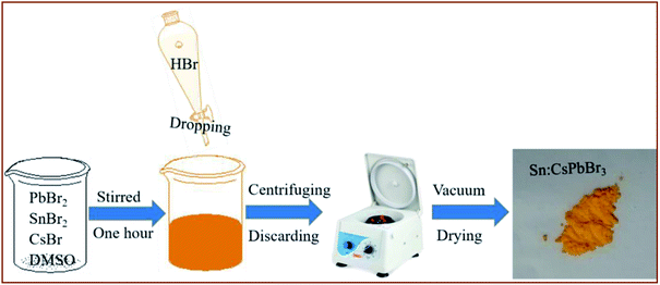 | ||
| Fig. 1 The schematic diagram of the synthesis of Sn:CsPbBr3 perovskite through a facile scheme by dropping hydrohalic acid into the precursor solution. | ||
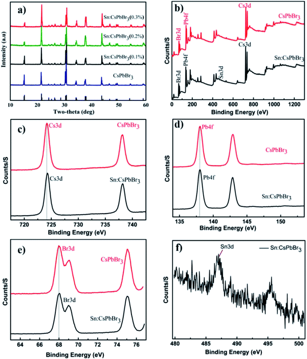
The X-ray powder diffraction (XRD) patterns of the CsPbBr3 perovskites powder with Sn (0%), Sn (0.1%), Sn (0.2%) and Sn (0.3%) doping concentrations are presented in Fig. 2(a). The XRD patterns of CsPbBr3 and Sn:CsPbBr3 perovskites with different Sn ion doping concentrations have strong diffraction peaks at 15°, 21°, 30°, 34°, 37° and 43°, which can be assigned to the representative peaks of CsPbBr3 perovskite lattice planes of (001)/(100), (110)/(−110), (002)/(200), (210)/(201), (211)/(−121) and (202)/(−220) respectively.38,39 Under varying concentrations of Sn ions, the perovskite materials have a good agreement to the undoped CsPbBr3 without any distinguishable peaks associated with the Sn ions. X-ray photoelectron spectroscopy (XPS) was performed to investigate the CsPbBr3 perovskite without and with Sn doping. The XPS of undoped CsPbBr3 perovskite and the individual peaks conforming of the Cs 3d, Pb 4f and Br 3d are presented in Fig. 2(b–e) in red. The Cs 3d, Pb 4f, and Br 3d spectra with their peak binding energy were revealed at 724.2, 138.02, and 68.05 eV respectively. Moreover, from the XPS spectra, we have examined that the atomic proportion of Cs/Pb/Br in the undoped CsPbBr3 was 14.46/15.35/70.19, respectively. In the same manner, the XPS spectra of Sn-doped CsPbBr3 and corresponding individual elements of Cs 3d, Pb 4f, Br 3d and Sn 3d are shown in Fig. 2(b–f) in black color. The separated elements of Sn-doped CsPbBr3 were assigned to Cs 3d, Pb 4f, Br 3d and Sn 3d spectra with their peak binding energies of 724.22, 138.04, 68.08 and 487 eV, respectively. After the doping of Sn, the resulting binding energies of Pb 4f and Br 3d increased, which resulted in an improved bonding of the CsPbBr3 perovskite. This improvement could help in the creation of steady and stabilized materials. The atomic proportion of Sn/Cs/Pb/Br in the Sn doped CsPbBr3 surveyed from the XPS spectra were 0.83/17.72/14.55/and 66.9, respectively.
The scanning electron microscopy (SEM) images of undoped CsPbBr3 and Sn doped CsPbBr3 perovskites powders are displayed in Fig. 3(a and b) at different magnification scale. The SEM images of the undoped CsPbBr3 from Fig. 3(a) showed less densely distribution compared to the corresponding SEM of Sn doped CsPbBr3 perovskite seen from Fig. 3(b). The Sn ion has a smaller radius than that of the Pb ion existing in the lattice gap of CsPbBr3, and the incorporation of Sn ion maybe regulating the typical dimensions of the CsPbBr3 perovskite. Therefore, the dimensions of Sn doped materials become improved compared to the undoped perovskite material and become significantly denser.
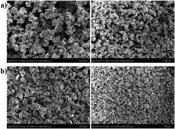 | ||
| Fig. 3 The SEM represent of as-synthesized perovskites powder (a) undoped CsPbBr3 and (b) Sn doped CsPbBr3 at different magnification scales. | ||
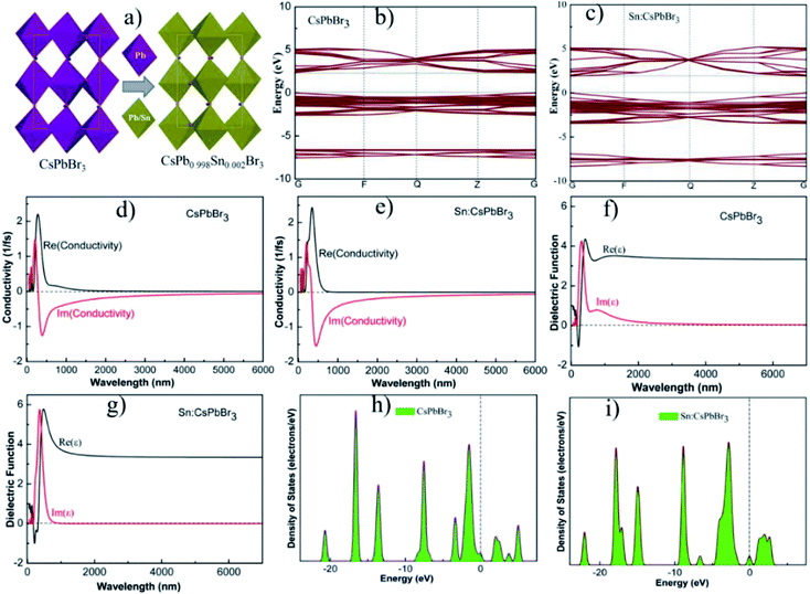
Theoretical schemes are employed using first principle calculations within the supportive system of generalized gradient approximation (GGA) and Perdew–Burke–Ernzerhof (PBE) functionals. The calculated band-gap energy of the optimized structure of CsPbBr3 and CsPb0.998Sn0.002Br3 perovskites were 2.3 eV and 2.2 eV, respectively, which suggested that the incorporation of Sn could tune the band gap energy.33,40 The schemes were achieved with the energy cutoff of 220 eV, and the total energy of 2 × 10⁻⁵ eV per atom with a maximum force of 0.05 eV Å−1. Fig. 4(b and c) shows the calculated band gap energy of the optimized structure of CsPbBr3 and CsPb0.998Sn0.002Br3 perovskites. Fig. 4(d and e) shows the conductivity of the undoped CsPbBr3 and doped CsPb0.998Sn0.002Br3 perovskites. The calculated conductivity of the doped perovskite in Fig. 4(e) was greater compared to the undoped CsPbBr3 perovskite shown in Fig. 4(d). The improvement in conductivity of doped perovskite may be ascribed to the alteration of bandgap energy.41 Moreover, the undoped CsPbBr3 and doped CsPb0.998Sn0.002Br3 perovskites dielectric functions are revealed in Fig. 4(f and g). Similar to conductivity, the dielectric functions of doped perovskite increased compared to the undoped perovskite materials. Fig. 4(h and i) shows the density of states (DOS) of the optimized structure of CsPbBr3 and CsPb0.998Sn0.002Br3 perovskites. Based on this analysis, the incorporation of small amounts of Sn could significantly improve the photovoltaic properties of all the inorganic perovskites.
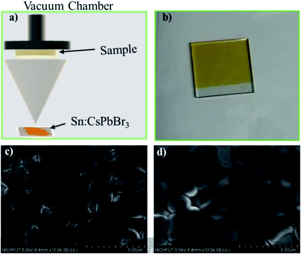
To further understand the Sn doping in perovskites, we fabricated PSCs using undoped and doped CsPbBr3 perovskite powder as precursor materials via direct thermal evaporation (Fig. 5(a)). Pinholes-free perovskite thin film was deposited on the TiO2-coated FTO glass. Fig. 5(b) shows the image of FTO/TiO2/Sn:CsPbBr3 substrate after thermal evaporation and post-annealing at 250 °C for 10 min. Smooth, constant and pinhole-free PSCs films are obtained through a proper deposition state. Top view SEM images of the undoped CsPbBr3 and Sn-doped CsPbBr3 perovskite thin-film are presented in Fig. 5(c) and (d), respectively. From the SEM images, we could determine that certain voids and pinholes existed in the undoped CsPbBr3 film layer, as shown in Fig. 5(c). From the figure, the intermediate grain size of the undoped CsPbBr3 perovskite film was reported to decrease compared to the doped perovskite film. In contrast, a pinhole- and void-free full coverage film was observed after the doping of Sn ion, as presented in Fig. 5(d). Moreover, the corresponding intermediate grain size of the Sn ion-doped CsPbBr3 perovskite film was enhanced compared to the pristine perovskite film. The intermediate grain size of the undoped CsPbBr3 film, as shown in Fig. S1a,† was close to 1.04 μm. The corresponding intermediate grain size of the Sn ion-doped CsPbBr3 film, as shown in Fig. S1b,† was 1.14 μm. When the Sn ion was introduced in CsPbBr3 film, the voids and pinholes reduced, and thus perhaps the minor crystal grains could fill-in the gap/voids between the large crystals grains, which condenses the pinholes of the perovskite layer and thus the continuity of the film was enhanced.33
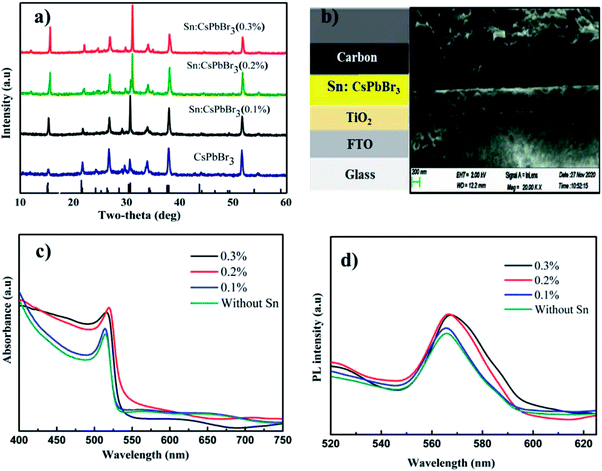
Fig. 6(a) shows the XRD patterns of undoped FTO/TiO2/CsPbBr3 and Sn-doped FTO/TiO2/Sn:CsPbBr3 thin film with different concentrations of Sn ion. The XRD designs of undoped FTO/TiO2/CsPbBr3 and Sn doped FTO/TiO2/Sn:CsPbBr3 thin film with different concentrations of Sn ion have similarity with the perovskite XRD discussed above, with the difference being that the film XRD have diffraction peaks at 26°, and 51°, which was related to the conductive FTO substrates. Fig. 6(b) shows the PSCs structure with a configuration of FTO/TiO2/Sn:CsPbBr3/carbon and the corresponding cross-sectional SEM image. Fig. 6(c) shows the optical absorbance spectra of the undoped and doped CsPbBr3 thin-film with different quantities of Sn ion. The absorption peaks of the CsPbBr3 perovskite thin film with different quantities of Sn ion doping was slightly shifted to the higher wavelength compared with the pristine CsPbBr3 perovskite thin-film absorption peaks. Similarly, Fig. 6(d) shows the photoluminescence (PL) spectra of the undoped and doped CsPbBr3 thin film with different quantities of Sn ion.
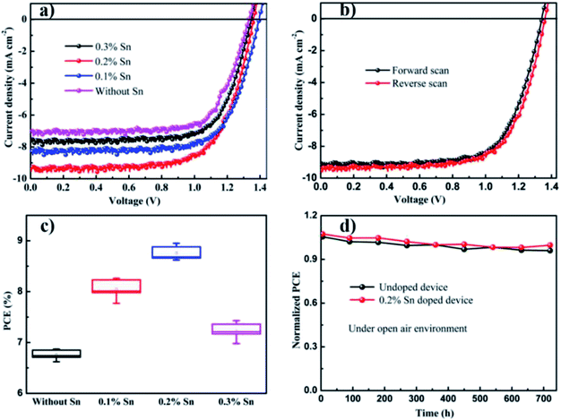
To realize the effect of Sn ion on the performance of CsPbBr3 solar cells, we introduced different amounts of Sn ion into the pure CsPbBr3-based solar cells. Fig. 7(a) shows the current density to voltage curvature of the undoped and Sn ion-doped at different doping amounts. Power conversion efficiency (PCE) and related solar cells parameters such as current density, open-circuit voltage and fill factor were calculated for undoped and Sn ion-doped perovskite solar cells. Fig. 7(a) shows the calculated PCE value of the undoped PSCs is about 6.87%, with current density (Jsc), open-circuit voltage (Voc) and fill factor (FF) of 7.08 mA cm−2, 1.33 V and 0.73, respectively. Through Sn ion doping with different concentrations, the PCE of devices and other parameters were enhanced. Thus, after doping with Sn (0.2%), the PCE value of the PSCs was increased to about 8.95% with Jsc of 9.27 mA cm−2, Voc of 1.36 V and FF of 0.71. Using a similar technique PCE of the PSCs at 0.1% Sn doping concentration was calculated about 8.26% with Jsc of 8.25 mA cm−2, Voc of 1.39 V and FF of 0.72. Moreover, at 0.3% Sn doping concentration, the calculated PCE of the PSCs was about 7.43% with Jsc of 7.65 mA cm−2, Voc of 1.35 V and FF of 0.72. The current density to voltage curvature for without/with Sn at different amounts along with the power conversion efficiency (PCE) and related solar cells parameters, such as current density, open-circuit voltage and fill factor, are discussed in Table 1.
| Sn ion | VOC [V] | JSC [mA cm−2] | FF [%] | PCE [%] |
|---|---|---|---|---|
| Without Sn | 1.33 | 7.08 | 0.73 | 6.87 |
| 0.1% Sn | 1.39 | 8.25 | 0.72 | 8.26 |
| 0.2% Sn | 1.36 | 9.27 | 0.71 | 8.95 |
| 0.3% Sn | 1.35 | 7.65 | 0.72 | 7.43 |
Therefore, the introduction of Sn ion might develop interface extraction of charge between the electron transport layer to perovskite and perovskite to the carbon. Fig. 7(b) shows the best accomplished J–V devices under forward and reverse scanning voltage is presented in with the calculated PCE value of 8.64% under forward and 8.95% under reverse scanning. The statistical distribution of PSCs parameters for pristine and Sn doped devices for a set of ten solar cells in Fig. 7(c) and S2† shows a slight deviation and high reproducibility via the direct deposition method described in this study.
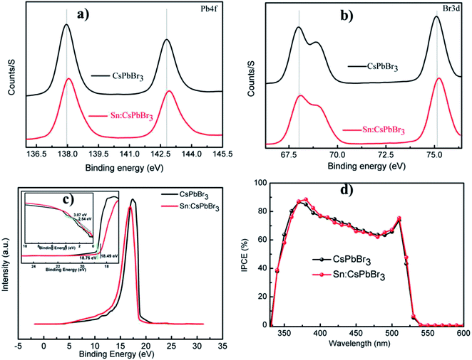
Moreover, higher stability under continual thermal and ambient air occurrence is a determined asset to be used in the commercial utilization of the PSCs devices. The solar cell's performances for the undoped CsPbBr3 and 0.2% Sn doped CsPbBr3 constructed PSCs in air is characterized over 720 h. Normalized solar cells PCE with storage time revealed in Fig. 7(d) are approximately unaffected over an operational period of 720 h. The result shown in Fig. 7(d) and after introducing Sn ions in the direction of the CsPbBr3 matrix, there is no noticeable negative result on the stability of the conforming device, even for slight advanced withholding values upon persistent open environment exposure compared to the undoped device performances. Recently, researchers presented that the environmental stability of all-inorganic perovskite solar cells performance is enhanced by metal ions doping due to lattice reduction.42 The incident photon-to-electron conversion efficiency (IPCE) spectrum of the devices presented in Fig. 8(d) show that the absorbable wavelength range of the pristine and with Sn introduced devices plateau between 350 and 530 nm. The maximum IPCE of about 80% was obtained in the wavelength range of 350 to 530 nm.
To understand the alteration of the bond energy of Pb and Br afterward introducing the Sn ion, we measured the XPS spectra to illustrate the perovskite film without and with Sn ion. The introduction of Sn ion in the perovskite lattice results in an increase in the bond energy of Pb and Br, as shown in the XPS spectral characterization of Pb 4f and Br 3d presented in Fig. 8(a and b). To examine whether the Sn ion influence the energy band structure of the CsPbBr3 perovskite material, we performed ultraviolet photoelectron spectroscopic (UPS) characterization of the CsPbBr3 perovskite films without and with Sn ion as presented in Fig. 8(c). The electronic structure of undoped and doped CsPbBr3 perovskite film measured by UPS has used an incident photon energy of 21.22 eV. The valence band maximum (VBM) boundaries of CsPbBr3 and Sn:CsPbBr3 perovskite materials films can be calculated using the equation: EVBM = 21.22 − (Ehigh − Elow).22 Hence, the calculated VBM results for CsPbBr3 perovskite films without and with Sn are 5.53 eV and 5.27 eV, respectively. The alteration of VBM value of the perovskite film after introducing Sn ion can gratify the energy construction orientation in the devices (Table 2).
| Method | Device structure | PCE [%] | Reference |
|---|---|---|---|
| Evaporation | FTO/c-TiO2/Sn doped CsPbBr3/carbon | 8.95 | This work |
| Evaporation | FTO/c-TiO2/CsPbBr3/carbon/CNT/MXene | 7.09 | 5 |
| Evaporation | FTO/c-TiO2/CsPbBr3/spiro-OMeTAD/Au | 8.65 | 20 |
| Evaporation | FTO/c-TiO2/CsPbBr3-CsPb2Br5/spiro-OMeTAD/Ag | 8.34 | 43 |
| Evaporation | FTO/c-TiO2/CsPbBr3/spiro-OMeTAD/Au | 6.95 | 19 |
| Evaporation | FTO/c-TiO2/CsPbBr3/Ti3C2-MXene/carbon | 9.01 | 44 |
| Laser deposition | FTO/c-TiO2/m-TiO2/CsPbBr3/spiro-OMeTAD/Ag | 6.30 | 15 |
| Solution | FTO/c-TiO2/m-TiO2/CsPbBr3/carbon-PANi/G | 8.87 | 1 |
| Solution | FTO/c-TiO2/m-TiO2/CQDs/CsPbBr3/RPQDs/carbon | 8.20 | 17 |
| Solution | FTO/c-TiO2/m-TiO2/SnBr2 doped CsPbBr3/carbon | 8.63 | 33 |
| Solution | ITO/TiO2/CoBr2 doped CsPbBr3/spiro-OMeTAD/Au | 8.57 | 34 |
Overall outcomes reveal that the direct deposition of Sn doped CsPbBr3 perovskite solar cells is promising to improve the environmental tolerance and photovoltaic performance of the all-inorganic PSCs.
Conclusions
In conclusion, undoped and Sn ion-doped CsPbBr3 perovskites were effectively synthesized and characterized through a facile scheme by adding hydrohalic acid toward the CsBr, PbBr2 and SnBr2 precursor in DMSO. The resulting Sn ion-doped CsPbBr3 perovskite was confirmed to be mass-scale, environmentally stable and highly crystalline material. Besides, using the dried Sn doped CsPbBr3 perovskite, the CsPbBr3 based PSCs were made-up through thermal evaporation. Thus, less-pinhole and continuous PSCs films were obtained through proper deposition in the form of FTO/TiO2/Sn:CsPbBr3/carbon. An impressive PCE of 8.95% was achieved after incorporation of Sn compared to the 6.87% efficiency of undoped CsPbBr3 perovskite. Overall, the advanced results argued that the direct deposition and Sn ion doping on CsPbBr3 in the synthesis phase pave an innovative strategy for potential photovoltaics.Conflicts of interest
There are no conflicts to declare.Acknowledgements
We acknowledge the National Natural Science Foundation of China No. U1632151, the Open Project of Jiangsu Key Laboratory for Carbon-Based Functional Materials & Devices (No. KJS1802), the Key Research and Development Project of Anhui Province of China (Grant No. 1704a0902023), and the Fundamental Research Funds for the Central Universities (No. JZ2019HGBH0202) for the financial support.References
- F. Bu, B. He, Y. Ding, X. Li, X. Sun, J. Duan, Y. Zhao, H. Chen and Q. Tang, Sol. Energy Mater. Sol. Cells, 2020, 205, 110267–110275 CrossRef CAS.
- D. Wang, W. Li, Z. Du, G. Li, W. Sun, J. Wu and Z. Lan, ACS Appl. Mater. Interfaces, 2020, 12, 10579–10587 CrossRef.
- P. Teng, X. Han, J. Li, Y. Xu, L. Kang, Y. Wang, Y. Yang and T. Yu, ACS Appl. Mater. Interfaces, 2018, 10, 9541–9546 CrossRef CAS.
- Y. Jiang, J. Yuan, Y. Ni, J. Yang, Y. Wang, T. Jiu, M. Yuan and J. Chen, Joule, 2018, 2, 1356–1368 CrossRef.
- L. Mi, Y. Zhang, T. Chen, E. Xu and Y. Jiang, RSC Adv., 2020, 10, 12298–12303 RSC.
- Y. Wang, X. Liu, T. Zhang, X. Wang, M. Kan, J. Shi and Y. Zhao, Angew. Chem., Int. Ed., 2019, 58, 16691–16696 CrossRef CAS.
- S. Shivarudraiah, M. Ng, C. A. Li and J. E. Halpert, ACS Appl. Energy Mater., 2020, 3, 5620–5627 CrossRef CAS.
- W. Ahmad, J. Khan, G. Niu and J. Tang, Sol. RRL, 2017, 1, 1700048–1700057 CrossRef.
- Y. Wang, T. Zhang, M. Kan, Y. Li, T. Wang and Y. Zhao, Joule, 2018, 2, 2065–2075 CrossRef CAS.
- B. Zhao, S.-F. Jin, S. Huang, N. Liu, J.-Y. Ma, D.-J. Xue, Q. Han, J. Ding, Q.-Q. Ge and Y. Feng, J. Am. Chem. Soc., 2018, 140, 11716–11725 CrossRef CAS.
- Q. Wang, X. Zheng, Y. Deng, J. Zhao, Z. Chen and J. Huang, Joule, 2017, 1, 371–382 CrossRef CAS.
- A. K. Jena, A. Kulkarni and T. Miyasaka, Chem. Rev., 2019, 119, 3036–3103 CrossRef CAS.
- G. Tong, L. K. Ono and Y. Qi, Energy Technol., 2020, 8, 1900961–1900978 CrossRef CAS.
- I. Poli, J. Baker, J. McGettrick, F. De Rossi, S. Eslava, T. Watson and P. J. Cameron, J. Mater. Chem. A, 2018, 6, 18677–18686 RSC.
- H. Wang, Y. Wu, M. Ma, S. Dong, Q. Li, J. Du, H. Zhang and Q. Xu, ACS Appl. Energy Mater., 2019, 2, 2305–2312 CrossRef CAS.
- H. Yuan, Y. Zhao, J. Duan, B. He, Z. Jiao and Q. Tang, Electrochim. Acta, 2018, 279, 84–90 CrossRef CAS.
- G. Liao, J. Duan, Y. Zhao and Q. Tang, Sol. Energy, 2018, 171, 279–285 CrossRef CAS.
- G. Liao, Y. Zhao, J. Duan, H. Yuan, Y. Wang, X. Yang, B. He and Q. Tang, Dalton Trans., 2018, 47, 15283–15287 RSC.
- J. Lei, F. Gao, H. Wang, J. Li, J. Jiang, X. Wu, R. Gao, Z. Yang and S. F. Liu, Sol. Energy Mater. Sol. Cells, 2018, 187, 1–8 CrossRef CAS.
- J. Li, R. Gao, F. Gao, J. Lei, H. Wang, X. Wu, J. Li, H. Liu, X. Hua and S. F. Liu, J. Alloys Compd., 2020, 818, 152903–152911 CrossRef CAS.
- H. Yuan, Y. Zhao, J. Duan, Y. Wang, X. Yang and Q. Tang, J. Mater. Chem. A, 2018, 6, 24324–24329 RSC.
- G. Tong, T. Chen, H. Li, W. Song, Y. Chang, J. Liu, L. Yu, J. Xu, Y. Qi and Y. Jiang, Sol. RRL, 2019, 3, 1900030–1900039 CrossRef.
- J. Duan, H. Xu, W. Sha, Y. Zhao, Y. Wang, X. Yang and Q. Tang, J. Mater. Chem. A, 2019, 7, 21036–21068 RSC.
- C. Liu, W. Li, H. Li, H. Wang, C. Zhang, Y. Yang, X. Gao, Q. Xue, H. L. Yip and J. Fan, Adv. Energy Mater., 2019, 9, 1803572–1803581 CrossRef.
- W. Chen, H. Chen, G. Xu, R. Xue, S. Wang, Y. Li and Y. Li, Joule, 2019, 3, 191–204 CrossRef CAS.
- J. Duan, Y. Zhao, B. He and Q. Tang, Angew. Chem., Int. Ed., 2018, 57, 3787–3791 CrossRef CAS.
- G. Tong, M. Jiang, D.-Y. Son, L. Qiu, Z. Liu, L. K. Ono and Y. Qi, ACS Appl. Mater. Interfaces, 2020, 12, 14185–14194 CrossRef CAS.
- G. Tong, T. Chen, H. Li, L. Qiu, Z. Liu, Y. Dang, W. Song, L. K. Ono, Y. Jiang and Y. Qi, Nano Energy, 2019, 65, 104015–104025 CrossRef CAS.
- G. Murugadoss and R. Thangamuthu, Sol. Energy, 2019, 179, 151–163 CrossRef CAS.
- X. Liu, X. Tan, Z. Liu, H. Ye, B. Sun, T. Shi, Z. Tang and G. Liao, Nano energy, 2019, 56, 184–195 CrossRef CAS.
- Y. Li, J. Duan, H. Yuan, Y. Zhao, B. He and Q. Tang, Sol. RRL, 2018, 2, 1800164–1800172 CrossRef.
- B. Parida, S. Yoon, S. M. Jeong, J. S. Cho, J.-K. Kim and D.-W. Kang, Sol. Energy Mater. Sol. Cells, 2020, 204, 110212–110241 CrossRef CAS.
- H. Guo, Y. Pei, J. Zhang, C. Cai, K. Zhou and Y. Zhu, J. Mater. Chem. C, 2019, 7, 11234–11243 RSC.
- D. Wang, W. Li, Z. Du, G. Li, W. Sun, J. Wu and Z. Lan, J. Mater. Chem. C, 2020, 8, 1649–1655 RSC.
- G. Tong, H. Li, G. Li, T. Zhang, C. Li, L. Yu, J. Xu, Y. Jiang, Y. Shi and K. Chen, Nano Energy, 2018, 48, 536–542 CrossRef CAS.
- G. Tong, X. Lan, Z. Song, G. Li, H. Li, L. Yu, J. Xu, Y. Jiang, Y. Sheng and Y. Shi, Mater. Today Energy, 2017, 5, 173–180 CrossRef.
- C.-Y. Huang, C.-C. Wu, C.-L. Wu and C.-W. Lin, ACS Omega, 2019, 4, 8081–8086 CrossRef CAS.
- L. Yang, T. Wang, Q. Min, B. Liu, Z. Liu, X. Fan, J. Qiu, X. Xu, J. Yu and X. Yu, ACS Omega, 2019, 4, 6084–6091 CrossRef CAS.
- X. Li, S. Chen, P.-F. Liu, Y. Zhang, Y. Chen, H.-L. Wang, H. Yuan and S. Feng, J. Am. Chem. Soc., 2020, 142, 3316–3320 CrossRef CAS.
- A. Bala and V. Kumar, J. Mater. Chem. C, 2019, 123, 6965–6969 CAS.
- C. Zhao, D. Huang, J. Chen, Y. Li and Z. Du, RSC Adv., 2016, 6, 98908–98915 RSC.
- S. Zou, Y. Liu, J. Li, C. Liu, R. Feng, F. Jiang, Y. Li, J. Song, H. Zeng and M. Hong, J. Am. Chem. Soc., 2017, 139, 11443–11450 CrossRef CAS.
- H. Li, G. Tong, T. Chen, H. Zhu, G. Li, Y. Chang, L. Wang and Y. Jiang, J. Mater. Chem. A, 2018, 6, 14255–14261 RSC.
- T. Chen, G. Tong, E. Xu, H. Li, P. Li, Z. Zhu, J. Tang, Y. Qi and Y. Jiang, J. Mater. Chem. A, 2019, 7, 20597–20603 RSC.
Footnote |
| † Electronic supplementary information (ESI) available. See DOI: 10.1039/d0ra09202a |
| This journal is © The Royal Society of Chemistry 2021 |

