
 Open Access Article
 This Open Access Article is licensed under a Creative Commons Attribution-Non Commercial 3.0 Unported Licence
Synthesis and electrochemical performance of silicon-nanowire alloy anodes
Edna Madosab,
Nimrod Harpaka,
George Levic,
Fernando Patolskya,
Emanuel Peleda and
Diana Golodnitsky *ac
*ac
aSchool of Chemistry, Tel, Aviv University, Tel Aviv, 6997801, Israel. E-mail: golod@tauex.tau.ac.il
bDepartment of Materials Science and Engineering, The Iby and Aladar Fleischman, Faculty of Engineering, Tel Aviv University, Tel Aviv, 6997801, Israel
cWolfson Applied Materials Research Center, Tel Aviv University, Tel Aviv, 6997801, Israel
First published on 3rd August 2021
Abstract
High-capacity materials are required in order to address the environmental concerns of our modern society, ultimately leading to safe and eco-friendly high-energy batteries. Silicon-nanowire anodes (SiNWs) have the potential to significantly increase the energy density of lithium-ion batteries (LIBs). In order to improve the mechanical durability and the electrochemical performance of SiNW-anodes, we fabricated a silicon–nickel (SiNi) composite anode by electroless deposition of nickel, followed by annealing at high temperature to obtain nickel silicides of different content and composition. The morphology of SiNi-alloy anodes was examined by SEM, in situ TEM and EDS methods in order to understand how different deposition protocols affect the coating of the silicon nanowires. The formation of Ni-silicides was found to occur during thermal treatment at 900 °C. Despite the incomplete shell coverage of SiNWs composed of multiple phases and grains, the electrochemical performance of binder-free and conducting-additive-free SiNi-alloy anodes showed stable electrochemical behavior and higher capacity retention compared to the pristine SiNW anode. Li/SiNW–SiNix cells ran at C/2 rate for 200 reversible cycles, exhibiting 0.1%/cycle capacity loss after completion of the SEI formation.
Introduction
The lithium-ion battery is the current leader in energy-storage devices because it has the highest volumetric- and gravimetric-energy density among known applied technologies. For the past decades, graphite has been used as a major anode material in Li-ion batteries because of its desirable properties, like long cycle life, low irreversible capacity, low volume expansion during lithiation and friendliness to the environment.1 However, the increase in energy-density and power-density requirements for Li-ion batteries for commercial applications, like portable electronic and vehicle industries, has led to a search for higher-capacity electrode materials. Silicon is an attractive candidate because it offers low discharge potential and high gravimetric capacity, nearly 11 times that of graphite. Its theoretical capacity is 4200 mA h g−1 (based on the stoichiometry of the Li22Si5 alloy) unlike graphite, that has a specific capacity of only 372 mA h g−1 (LiC6).2Unfortunately, in order to integrate silicon-based anodes in commercial batteries, there are a number of challenges to overcome. Silicon-based anodes experience structural volume changes of up to 280%.3 This induces powerful stress in the silicon anode and often leads to pulverization of the active material and the loss of electrical contact during lithiation–delithiation. The large volume change can also crack the initially formed solid–electrolyte-interphase (SEI) layer. This is accompanied by a continuous reduction reaction of liquid electrolyte followed by the formation of a fresh SEI, and thus keeping the SEI films growing during cycling. Eventually it leads to the degradation of the cell performance by high, irreversible capacity (Qir) loss and poor faradaic efficiency.4
To solve this problem and improve the electrochemical performance of silicon-based anodes, some solutions were suggested. The most common solution to deal with Si pulverization is to reduce the particle dimensions of the electrode material down to the nanoscale. Recently, various LIBs based on Si powders,5–7 Si composites,8,9 Si nanotubes10 and Si nanowires (SiNW)11–13 have been reported. Si nanostructures have the advantage of a higher surface-to-volume ratio, as well as shorter diffusion distance for lithium ions, which can help in reducing the volume expansion during lithiation/delithiation and improve the power capability and cycling performance14 of the battery. There is a critical nanostructure size of ∼150 nm for particles15 and ∼300 nm16 for SiNW, below which the nanostructures remain uncracked and intact upon cycling.
In addition, synthesizing silicon composites with various structures and coatings is another common approach to controlling volume expansion during lithiation/delithiation, protecting the electrode surface from being reactive towards the electrolyte and improving the cyclability of silicon-based anodes. For example, Sethuraman et al. investigated the effect of copper coating on thin silicon film and found that the presence of copper coating contributes to the higher cycling efficiency and rate capability of silicon electrodes, in addition to minimizing the overall capacity loss resulting from pulverization.17 Lotfabad et al. achieved performance improvement by coating silicon nanowire anodes with TiO2 by atomic-layer deposition (ALD).18 Huang et al. coated silicon particles by nickel in a sputter-coater followed by heat treatment for the formation of silicide coating, and showed improvement in capacity retention.19 Our group recently found that coating silicon nanoparticles by a nickel electroless-plating procedure, followed by thermal treatment for Ni silicide formation, results in a high capacity-retention rate and high C-rate capability. The Si–Ni anodes exhibited a reversible capacity of about 620 mA h g−1 Si at 120 μA cm−2 at cycle 210, and 800 mA h g−1 Si at 50 μA cm−2 at cycle 240.5 Electroless plating is characterized by the selective reduction of metal ions at the surface of a catalytic substrate immersed in an aqueous solution containing the cations of the metal to be deposited in the presence of a reducing agent. The benefit of this process over the electroplating process is the uniform coating observed on complex shapes and the fact that no external electrical source is required.20
We have recently described the SiNW anodes grown directly on a flexible, open-structure stainless-steel current collectors by a novel one-step catalyst-free chemical-vapor-deposition process. The anode appears as a binder-free silicon sponge-like network21 and can be cycled for more than 500 cycles with <50% capacity loss at 0.1 mA (C/6 rate). We present here an attempt to create nickel silicides shell structures on top of silicon-nanowire-based anodes for further improvement of their electrochemical performance in lithium-ion batteries (e.g. high capacity retention). Nickel silicides shells on SiNW core structures were prepared via electroless nickel deposition, followed by thermal treatment. This is to the best of our knowledge the first demonstration on the application of free-of-binder Si-core/nickel silicide shell nanowire electrodes as anodes for lithium-ion battery applications.
Results and discussion
Electroless deposition of nickel on SiNW anode
To determine, which electroless deposition bath and plating conditions are the most suitable for coating of SiNW anodes, four different bath compositions, which contained NiSO4·6H2O, Na3C6H5O7·2H2O and NaPO2H2 H2O at different concentrations, were tested under different operating conditions as listed in Table 1. According to literature data, NiSi and NiSi2 compounds deliver, relatively to pure Si, lower theoretical capacities of 1360 and 562 mA h g−1, respectively.22 Despite the decreased capacity, as compared to pristine silicon, we believe that a thin layer of nickel silicides has great potential as a protector of the SiNW anode surface. Nickel silicides have higher electrical conductivity and in addition, are expected to limit the large volume change during lithiation–delithiation, the destruction of the initially formed SEI layer, the pulverization of the anode and the loss of SiNW contact with the current collector. Therefore, the guideline for choosing the optimal bath and plating conditions was the capability to provide a thin nickel coverage layer and to eliminate complete transformation of the silicon nanowires to nickel-silicide nanowires during the silicidation step. The latter would result in a high capacity drop. To quantify and estimate the average diameter size of the deposited nickel spheroids based on their cross-sectional area, ImageJ open-source image-analysis software toolboxes24 was used. First, the nickel plating was performed in bath 1 under two different operating conditions, at pH 8 and a temperature of 55 °C, and at pH 10 and 70 °C for deposition times of 30 and 60 seconds. At pH 8 the nickel deposit is thin, and the coating is non-uniform. The ESEM images of a pristine silicon nanowire anode at different magnifications are shown in Fig. 1a–d. The nickel coated nanowires can be seen in Fig. 1e–h. The average diameter of nickel spheroids deposited from bath 1 at pH 8 is about 57 nm after 60 seconds of immersion (Fig. 1f). 30 seconds of electrode immersion does not provide coating at all (Fig. 1e). At pH 10, the globule size of nickel deposits ranges from ∼127.5 to ∼299.3 nm after 30 and 60 seconds, respectively (Fig. 1g and h).| Constituents of the bath (M) | Concentrations | |||
|---|---|---|---|---|
| Bath 1 | Bath 2 | Bath 3 | Bath 4 | |
| NiSO4·6H2O | 0.12 | 0.12 | 0.06 | 0.12 |
| Na citrate | 0.14 | 0.24 | 0.24 | 0.24 |
| NaH2PO2 | 0.36 | 0.36 | 0.36 | 0.72 |
| NH4OH | A few drops to obtain the desirable pH value | |||
| Operating conditions | ||||
|---|---|---|---|---|
| Temperature [°C] | 55, 70 | 70 | 70 | 70 |
| PH | 8, 10 | 10 | 10 | 10 |
| Plating time [s] | 30/60 | 60/120 | 60/120 | 30/60/120 |
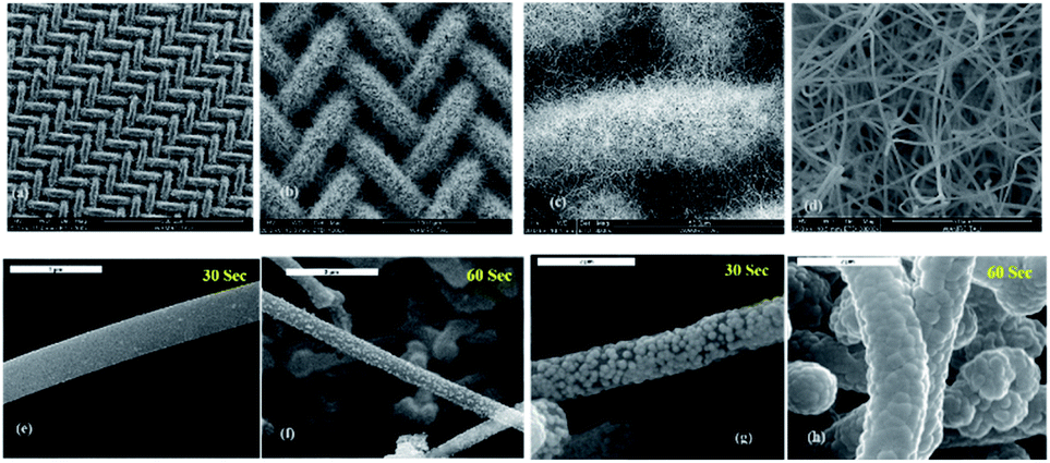 | ||
| Fig. 1 SEM images of neat SiNWs at different magnifications and SiNWs coated by Ni under different operating conditions in bath 1. (e and f) pH-8, temp-55 °C; (g and h) pH-10, temp-70 °C. (e and g) 30 seconds of plating; (f and h) 60 seconds of plating. | ||
It is apparent that at pH 10, the deposition rate increases sharply and leads to greater thickness and larger Ni spheroids as opposed to the deposits obtained at pH 8. In addition, a 60 second immersion at pH 10 ensures full coverage of the nanowire surface. High temperature and pH level appear to accelerate the process and affect the thickness of the resulting coating layer. On the basis of these results, pH 10 and 70 °C have been chosen for testing the effect of the ratio between the concentrations of Ni2+, complexing and reducing agents on the Ni-on-SiNW morphology (baths 2, 3 and 4, Table 1).
Fig. 2 shows the effect of concentration of different agents in the electroless-nickel bath on the morphology of nickel and the deposition rate. Following our previous studies25 focused on the electroless deposition of nickel on high-surface-area perforated silicon wafers and glass capillary arrays, we tested here the effect of the concentration of nickel salt, complexing and reducing agents on the deposition rate and morphology of coatings formed on silicon nanowires. The relative content of bath components varied from 1.17![[thin space (1/6-em)]](https://www.rsc.org/images/entities/char_2009.gif) :1 to 4:1 (C6H5O7−:Ni2+) and from 3:1 to 6:1 (PO2H2−:Ni2+). We found that the spheroids size of the nickel coating on silicon decreases from ∼299.3 nm to ∼71.8 nm with doubling of the concentration of citrate (bath 1 vs. bath 2). However, full coverage of SiNWs was achieved only after the process lasted 120 seconds.
:1 to 4:1 (C6H5O7−:Ni2+) and from 3:1 to 6:1 (PO2H2−:Ni2+). We found that the spheroids size of the nickel coating on silicon decreases from ∼299.3 nm to ∼71.8 nm with doubling of the concentration of citrate (bath 1 vs. bath 2). However, full coverage of SiNWs was achieved only after the process lasted 120 seconds.
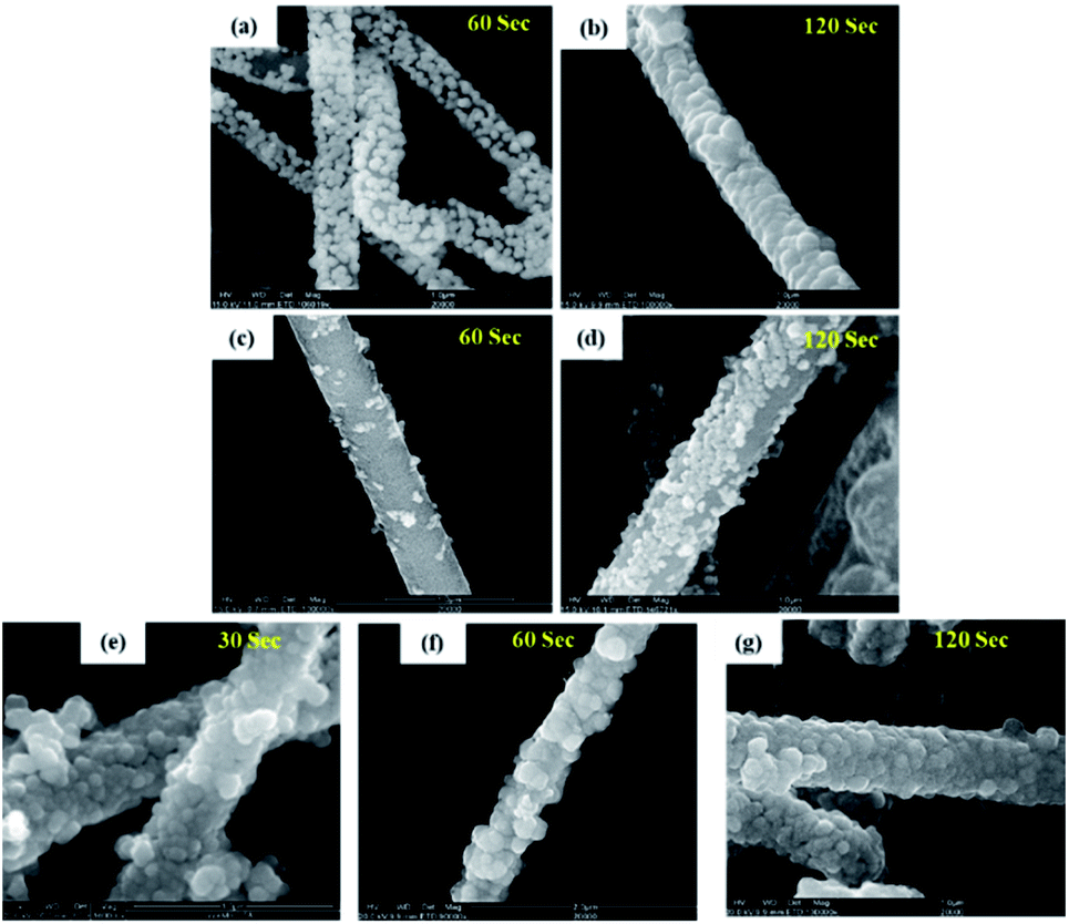 | ||
| Fig. 2 SEM images of plated SiNWs coated in different baths and different deposition times (pH-10, 70 °C) (a and b) bath 2 (c and d) bath 3 (e–g) bath 4. | ||
Lowering of the concentration of nickel sulfate to 0.06 M (bath 3) while leading to the formation of extremely small nickel spheroids (Fig. 2c and d) causes uneven nickel coverage of the SiNWs. High-content sodium hypophosphite (bath 4) followed by an increase in the reaction rate, and in the spheroid dimensions from ∼71.8 nm to ∼91.8 nm. The coating becomes much thicker, denser and completely covers the SiNWs. In an attempt to obtain a thinner layer that still fully covers the silicon nanowires, we repeated the test with a shorter immersion time of 30 seconds (bath 4) and were able to obtain SiNWs completely coated by nickel particles of about 71.5 nm size (Fig. 2e).
Nickel-silicide formation by thermal treatment
In the present work, Ni diffusion into SiNWs followed by the formation of nickel silicides was studied under thermal treatment by in situ transmission electron microscopy (TEM) equipped with TEM heating sample holder.Fig. 3 shows the TEM images of the selected nickel-coated nanowires at 25, 650, 700, 750, 800, 850 and 900 °C. The main challenge in obtaining a silicide coating on the SiNWs is the native silicon dioxide layer that covers silicon. TEM analysis performed on the nickel-coated SiNW anode prior to thermal treatment, shows that nickel particles deposit on about 2 nm thick native silicon dioxide layer as can be seen in Fig. 4. This observation was also confirmed by EELS data (Fig. 5). EELS test conducted after the thermal treatment of nickel-coated SiNWs at 650 °C shows the absence of silicides. The oxygen content is significantly higher at the interface between the nickel coating and silicon nanowire, strongly suggesting that both the SiNW and nickel surfaces are oxidized. These findings confirm our TEM observations (Fig. 3) that the oxide layer functions as a barrier between the SiNW and the nickel coating. At temperatures lower than 900 °C, nickel showed no signs of reacting with silicon dioxide. At about 650 °C, nickel particles begin to agglomerate and form nickel islands on top of the SiNW surface.
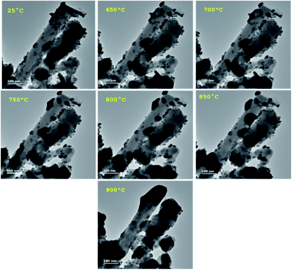 | ||
| Fig. 3 TEM images showing in situ TEM thermal treatment process of Ni-coated silicon nanowires. | ||
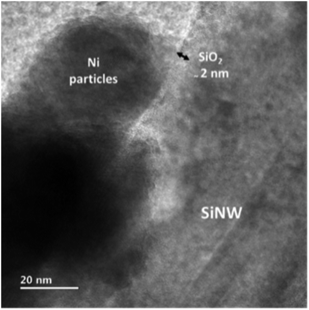 | ||
| Fig. 4 TEM image of nickel particles on top of the SiNW oxide at room temperature before thermal treatment. | ||
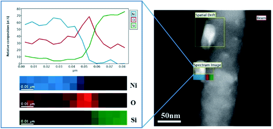 | ||
| Fig. 5 STEM-EELS elemental mapping of nickel particles on top of the SiNW oxide at room temperature before thermal treatment. | ||
Above 750 °C, the agglomeration continues, and non-homogeneous dispersion of nickel clusters over the surface is clearly visible. Only at 900 °C, after 20 minutes of treatment, does the penetration of nickel into the silicon become visible. Since the atomic mass of nickel is higher than that of silicon, the deposited nickel layer appears darker than the silicon nanowires (Fig. 6). When the temperature reaches 900 °C, SiNW turns dark as a result of nickel penetration. In addition, the grain boundaries of nickel crystallites blur with increasing temperature.
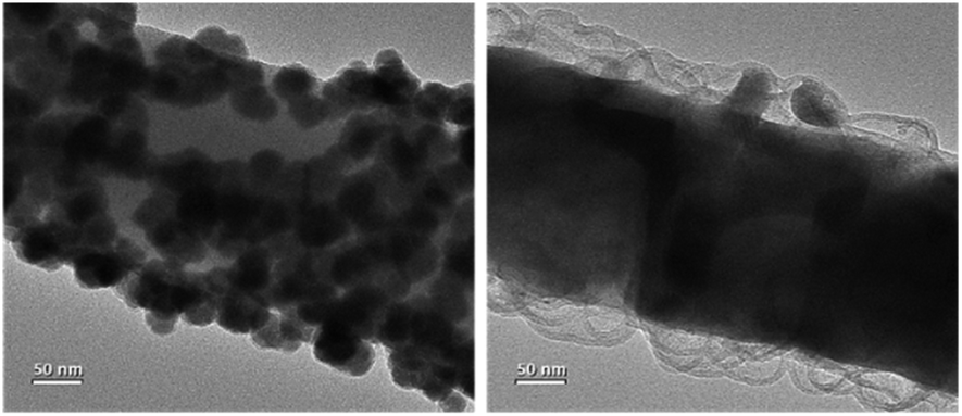 | ||
| Fig. 6 Ni penetration and silicide formation at 900 °C. (a) Ni particles on SiNW before thermal treatment (b) Ni penetration at 900 °C after 20 minutes. | ||
As mentioned by Dallaporta,26 nickel has no thermodynamically favorable reaction products with SiO2 up to 900 °C. In order to react with silicon, nickel must reach a neat silicon surface.26 Liehr et al.27 reported that nickel coating reacts with silicon underneath the SiO2, via defects and/or voids in the oxide, through which the metal can diffuse to the SiO2/Si interface and form silicide layers.
Another study reports that no diffusion of nickel through the oxide occurs below 800 °C.28 Nielsen et al.29 detected 10–20 Å-sized voids in silicon oxide, with the use of positron beams. We have found by in situ TEM that formation of voids begins at 850 °C, thus enabling partial penetration of nickel through a ∼2 nm-thick oxide layer. At 900 °C, silicon oxide decomposes to form volatile SiO, which desorbs from the surface and leaves an array of expanding voids in the SiO2 layer. Nucleation of nickel atoms occurs in these oxide nano- and microvoids, diffuses into the bulk of silicon and, finally creates nickel silicides.
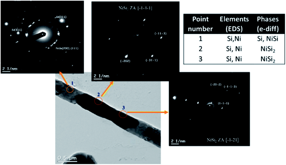
Fig. 7 shows selected-area electron-diffraction (SAED) patterns of nickel-coated SiNWs after thermal treatment at 900 °C, carried out during UHR TEM measurements. The presence of nickel silicides was observed in all the selected areas. Both the electron-diffraction patterns and EDS data indicate high content of NiSi2 phase (Fm![[3 with combining macron]](https://www.rsc.org/images/entities/char_0033_0304.gif) m, a – 5.406 Å) with atomic ratio of 1:2 Ni:Si. Nano-size particles of NiSi phase (Pnma, a – 5.18 Å, b – 3.34 Å, c – 5.62 Å) were found in these regions as well.
m, a – 5.406 Å) with atomic ratio of 1:2 Ni:Si. Nano-size particles of NiSi phase (Pnma, a – 5.18 Å, b – 3.34 Å, c – 5.62 Å) were found in these regions as well.
 | ||
| Fig. 7 A series of electron diffraction patterns obtained from the sample after in situ TEM thermal treatment at 900 °C. | ||
Electrochemical performance
The electrochemical performance of the NiSix–SiNW composite electrodes was tested in half-cells with the use of coin-cell batteries with 12 mm-diameter lithium anodes. In addition, a control test was performed by assembling half-cells with pristine SiNW electrodes. The cells were cycled at a relatively low current density of 0.1 mA cm−2 (C/20) for three cycles, in order to extract their maximum capacity. The following 97 cycles were carried out at 1 mA cm−2 (C/2), which remained constant for both charge and discharge until the 100th cycle, after which the current density was lowered to 0.1 mA cm−2 for three cycles. In all half-cells, the voltage range was 0.05–1 V.Fig. 8 shows the capacity vs. cycle number curves of the half-cells comprising NiSix composite electrode after thermal treatment at 900 °C as compared to the cell with pristine SiNW anode. The cell with NiSix–SiNW electrode demonstrates lower reversible capacity values than the cell with the reference electrode. The NiSix–SiNW electrode shows initial delithiated capacity of 1191.9 mA h gSi−1, while the pristine SiNW electrode has an initial capacity of 2426.9 mA h gSi−1. The reduction in the reversible capacity values obtained for the NiSix–SiNW samples can be attributed to the reduced amount of neat silicon as a result of the formation of NiSi and NiSi2 phases (as described in the previous section). According to literature data, NiSi2 and NiSi silicides produce, on lithium alloying/de-alloying, lower theoretical capacities of 562 and 1360 mA h g−1, respectively.22 Despite the decreased initial capacity, the formation of nickel silicides was found to enhance the cycling performance of the samples; the NiSix–SiNW anode shows much more stable behavior during cycling compared to the pristine SiNW anode. As can be seen in Table 2, the NiSix–SiNW anode showed much lower capacity loss at higher cycle numbers (at a high current density of 1 mA cm−2) compared to the pristine anode. It showed 16.1% capacity loss at cycle 75 and 25.4% capacity loss at cycle 100, whereas the pristine anode shows capacity losses of 34.8% and 48.5%, respectively. Another interesting phenomenon is the differences in the capacity losses of the samples at the lower current density of 0.1 mA cm−2. After 102 cycles, in comparison with cycle 2, the NiSix–SiNW anode lost 3.2% of its initial capacity, whereas the pristine anode lost 10.1% of its capacity. The electrochemical deterioration of the pristine anode is much more rapid and noticeable. This is a strong indication that negligible pulverization occurred during the first 100 cycles of the NiSix–SiNW anode.
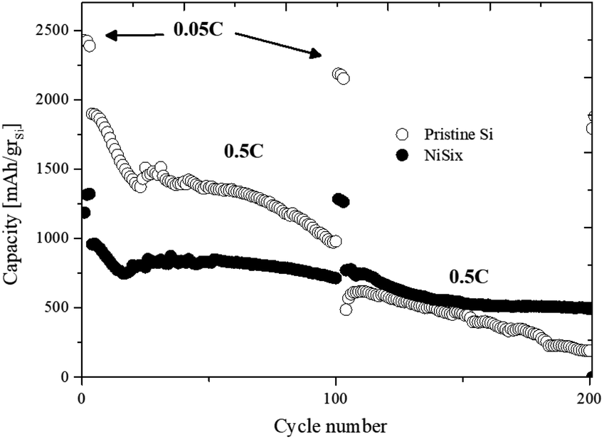 | ||
| Fig. 8 The cycle life of Li/SiNW and Li/SiNW–Ni cells. | ||
| Cycle number | C rate | Capacity loss [%] | |
|---|---|---|---|
| NiSix | Pristine SiNW's anode – Ref. | ||
| 50 | C/2 | 13.6 | 28.1 |
| 75 | 16.1 | 34.8 | |
| 100 | 25.4 | 48.5 | |
| 150 | 44.4 | 75.9 | |
| 102 | C/20 | 3.2 | 10.1 |
In order to follow much more clearly the effect of cycling on the electrochemical behavior, dQ/dV plots (Fig. 9) of NiSix–SiNW and pristine SiNW anodes were constructed for low and high current-density charge/discharge. Each peak feature represents a different electrochemical reaction and the area under the peak is the capacity of the particular process.30 Fig. 9a and b, which present the cycling at low current density (C/20-rate), show that during delithiation, two dQ/dV peaks are typically observed. The dQ/dV peak at about 270 mV corresponds to the transformation of the lithium-rich a-Li3.5Si phase to amorphous lithium silicide of a-Li2.0Si composition and the dQ/dV peak at about 500 mV corresponds to the transformation of the a-Li2.0Si phase to the amorphous a-Si.31 In addition, two lithiation peaks observed at about 100 and between 250–300 mV are ascribed to the gradual lithiation of large clusters of silicon to amorphous lithium silicide (a-Li2Si) that possibly includes two distinct processes (two overlapping peaks appeared). This is followed by the conversion of a-Li2Si to amorphous Li3.5Si phase, assisted by the formation of small clusters of silicon by further breakup of the Si–Si bonds.31 In the low C-rate dQ/dV plots of SiNW anodes (Fig. 9a), it can be seen that the intensity of the delithiation peak of cycle 2 (C/20) at 270 mV, is stronger than the delithiation peak at 500 mV. We attribute the changes in the peaks to kinetic influences. At higher current density, the α-Li2Si to α-Si delithiation transform (∼500 mV peak) has faster kinetics and dominates that of the α-Li3.5Si to α-Li2Si transformation (∼270 mV peak). This is followed by an increase in the charge/discharge overpotential. The dQ/dV curves of cycle 102 and cycle 2 almost coincide in the cell with the NiSix–SiNW electrode. The height of the peak and the overpotential do not change at all. Fig. 9c and d show cycling of the cells at high current density (C-rate C/2). Some buildup of overpotential during cycling is readily observed in the dQ/dV plots of the anodes in comparison with the peaks at low current density (Fig. 9a and b). The stronger overpotential accumulation was detected during the first cycles as a result of SEI formation, as we are already discussed in our previous findings.11,32 Growth of the SEI layer is promoted during lithiation but suppressed during delithiation and requires more than a single cycle to reach a steady state, which results in high capacity fade during the first ∼25 cycles, as is readily observed in the cycle-life plot of the anodes (Fig. 8). This high capacity drop that occurs due to the growth and stabilization of the SEI layer is reflected in a sharp decrease (or even disappearance) of the Li-rich phase peak starting from cycle 20 in the lithiation/delithiation dQ/dV plot (Fig. 9c and d) of the pristine and NiSix–SiNW anodes, respectively. This process was observed in the dQ/dV plots of all the following cycles. In the first cycles (at high current density) it is reasonable to assume that it is easy for the lithium ions to diffuse through the SiNW bulk and form the Li-rich phase (cycle 5), because the SEI layer is very thin. Later, with secondary SEI growth and stabilization11 (up to cycle ∼25), which is followed by a sharp increase in the lithiation overpotential, the SEI acts as a diffusion barrier for lithium-ion penetration and results in deceleration of the lithium diffusion.
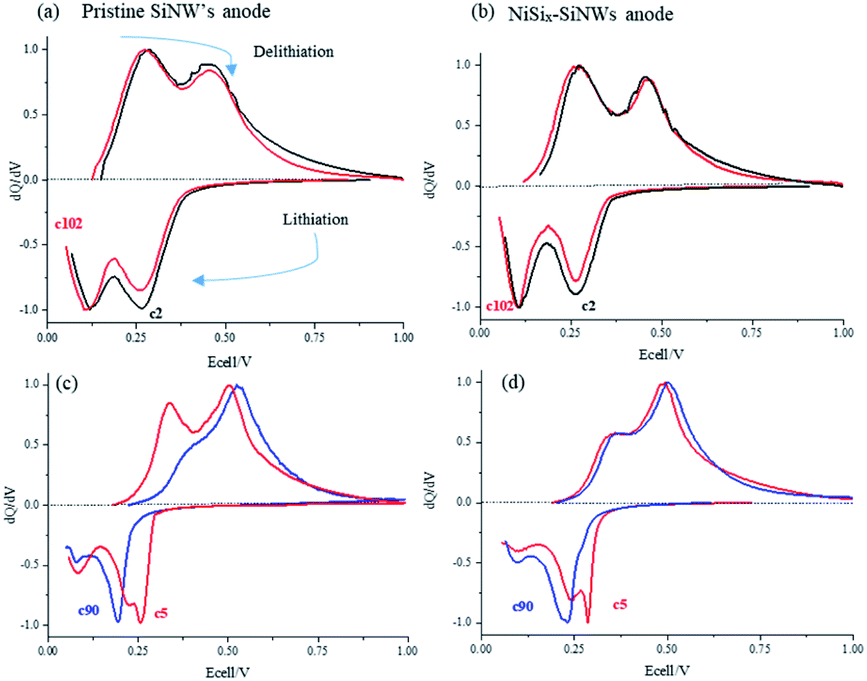 | ||
| Fig. 9 Normalized differential capacity plots of Li/Si cells comprising pristine and nickel-coated SiNW anodes. C/20 rate (a and b) and C/2 rate (c and d) for cycles 2, 5, 90 and 102. | ||
In addition, because of the short time of the lithiation step, at high current density with the combination of a thicker SEI layer only a small amount of lithium-ions manages to diffuse into the electrode during the deposition step. This leads to the only dominant transition from silicon to lithium-poor silicides that occurs between cycles 5 and ∼25, whereas the Li-rich phase-transformation peak disappears. After 200 cycles at C/2-rate the average lithiation/de-lithiation overpotential increases from 90 to 182 mV and from 89 to 135, in the cell comprising pristine SiNW and electrode with NiSix–SiNW electrode, respectively. A continuous capacity degradation (∼0.5%/cycle from cycle 5 to cycle 200) observed for the pristine anode and much better capacity retention (∼0.2%/cycle capacity loss), exhibited by NiSix–SiNW anode can be attributed to higher mechanical strength of nickel silicide structure, which prevents cracking of the anode upon expansion/contraction during cycling. Electroless coating of silicon nanowires anode, followed by thermal treatment triggers Ni to react with the surface Si, thus forming a silicide coating layer chemically bonded to SiNWs. Unlike physically coated layers that typically can crack and detach from Si surfaces upon repeated cycling, NiSix remains connected with the bulk SiNWs as a skin-like protective surface. This, in turn, eliminates growing of the SEI from upon cycling, in agreement with,11,32–35 and together with higher electrical conductivity of nickel silicide as compared to neat silicon, may explain the small changes observed in the lithiation/delithiation overpotential.
Conclusions
Silicon nanowire electrodes underwent electroless deposition of nickel, followed by annealing at high temperature to obtain a core–shell structure composed of SiNW core and a metal silicide crystalline-shell layer of incomplete shell coverage. The effect of the relative content of nickel salt, complexing and reducing agents on the deposition rate and morphology of the coating was tested. The composition of the bath containing 0.12 M NiSO4, 0.24 M Na3C6H5O7, 0.72 M NaH2PO2, NH4OH, and operating conditions of pH 10, 70 °C and 30 seconds plating time have been chosen as the optimal conditions for nickel coating of the SiNW anodes. The choice was made to enable conformal and thinnest Ni coating and to ensure that not all the silicon nanowires will be transformed in the following thermal treatment step into fully Ni-silicide NWs.The morphology of SiNi alloy films was examined by SEM, TEM and EDS methods. The results show the formation of Ni-silicides during the thermal treatment at 900 °C. The shell coverage is composed of multiple phases and grains. Examination of the electrochemical performance of the SiNi alloy anodes showed stable electrochemical behavior and high capacity retention compared to the pristine SiNW anode.
We suggest that NiSix acts as a protective coating layer for the SiNWs. Since the nickel silicide is an electrochemically inactive phase, the overall capacity of the silicon-nanowire anode decreases. The lower amount of silicon involved in reversible charge/discharge, is reflected in the smaller volumetric change of the SiNWs during cycling. This can explain high capacity retention and low overpotential of the NiSix–SiNW anode.
Experimental
Fabrication of SiNW anodes
The SiNW anodes were synthesized by a catalyst-free CVD process as described in our previous study.21 316L-grade stainless-steel mesh of 25 μm-thick fibers was immersed in 40% HF solution (Merck, Sigma-Aldrich). The mesh was then rinsed with DI water, dried and put inside the CVD chamber. Once inside the quartz tube, the chamber was evacuated to base pressure (5 mTorr) followed by the introduction of silane (SiH4) at a flowrate of 5 sccm and diluted with argon gas carrier (flowrate of 20 sccm), at 470 °C, for a growth time of two hours.Electroless Ni plating
Since silicon is a semiconductor, prior to nickel coating the SiNW anodes were subjected to sensitization and activation steps. Sensitization of the samples was carried out in a 20g L−1 SnCl2·2H2O and 40 mL HCl (32%) solution with the use of a magnetic stirrer for one minute, followed by rinsing of the samples in distilled water. Following this, the anodes were activated in a solution containing 1.5g L−1 PdCl2 and 1.5 mL L−1 HCL (32%), with the use of a magnetic stirrer for one minute, and then washed with distilled water.23An alkaline plating bath, which contains different concentrations of the following constituents, was used: NiSO4·6H2O (nickel sulfate), Na3C6H5O7·2H2O (sodium citrate), NaPO2H2 H2O (sodium hypophosphite). First, the nickel sulfate and sodium citrate were added to 50 mL of distilled water. After these salts dissolved, a few drops of ammonium hydroxide were added to obtain the desired pH value, which was continuously controlled around 10, and then the sodium hypophosphite was added. The plating was conducted at 55 or 70 °C for 30 seconds. After the plating process was completed, the anodes were rinsed with distilled water and dried in air.
Formation of Ni silicides by thermal treatment
To form nickel silicides, the anodes were heated at a rate of 10°C min−1 in a CARBOLITE horizontal-tube furnace under nitrogen gas (99.999% N2) for two hours, at different temperatures, from 650 to 900 °C.Preparation of electrodes and assembly of coin cells
The anodes were cut into 12 mm – diameter discs and were dried under vacuum for 12 hours at 50 °C and 2 hours at 100 °C. The mass loading of the anodes was 2 mgSi cm−2. CR2032 coin cells were assembled inside a glovebox filled with ultra-high-pure argon (content of O2 and H2O < 0.1 ppm). The coin cell contained a silicon anode, a 2400 Celgard separator (19 mm diameter) and a lithium-foil counter electrode (15 mm in diameter). About 100 μL of electrolyte was added the coin cell. The electrolyte contained 1MLiPF6 in EC:DEC (1:1) with 2% (v/v) VC and 15% (v/v) fluoroethylene carbonate (FEC). After sealing, the coin cells were taken out of the glove-box and were tested in a Biologic BCS-805 cycler. The cells were cycled over a voltage range of 1–0.05 V. Each charge and discharge is followed by the 5 min rest step under zero-current conditions. The results were analyzed with the EC-lab (Biologic software).
Microscopy characterization of the samples
A JSM-6300 scanning microscope (Jeol Co.) equipped with a Link elemental analyzer and a silicon detector, was used for the study of the surface morphology of the electrodes. TEM images of the samples were taken with a FEI™ F20 Philips-Tecnai TEM and JEOL™ JEM-2010F FEG-STEM. STEM-EELS (electron-energy-loss spectroscopy) was conducted with a JEOL JEM-2010F UHR operated at 200 kV, equipped with EELS (Tridiem 863, made by Gatan)In order to analyze the Ni-coated SiNWs for TEM characterization, the anode was only partly covered with nickel in order to be able to distinguish the penetration stage of the nickel. Following this, the coated SiNW anode was placed in an Eppendorf tube filled with ethanol and by sonication, the nickel-covered nanowires were detached from the stainless-steel-mesh substrate. With the use of a pipette, the resulting solution was dripped onto the TEM grid. The nanowires were analyzed after evaporation of the ethanol. The temperature of the TEM holder was increased at a rate of 20 °C min−1, from room temperature up to 900 °C. From 650 °C, after every elevation of 50 °C, the heating was paused, and the thermal drift was stabilized for a 20 minute period.
Conflicts of interest
There are no conflicts to declare.Acknowledgements
This work was partially supported by the Planning & Budgeting Committee of the Council of High Education and the Prime Minister Office of Israel, in the framework of the INREP project and by Momentum Fund, Ramot.References
- M. Winter, J. O. Besenhard, M. E. Spahr and P. Novak, Adv. Mater., 1998, 10, 725–763 CrossRef CAS.
- T. D. Hatchard and J. R. Dahn, J. Electrochem. Soc., 2004, 151, A838 CrossRef CAS.
- M. N. Obrovac and L. J. Krause, J. Electrochem. Soc., 2007, 154, A103 CrossRef CAS.
- E. Peled and S. Menkin, J. Electrochem. Soc., 2017, 164, A1703–A1719 CrossRef CAS.
- K. Goldshtein, K. Freedman, D. Schneier, L. Burstein, V. Ezersky, E. Peled and D. Golodnitsky, J. Electrochem. Soc., 2015, 162, A1072–A1079 CrossRef CAS.
- N. Liu, H. Wu, M. T. Mcdowell, Y. Yao, C. Wang and Y. Cui, Nano Lett., 2012, 12, 3315–3321 CrossRef CAS PubMed.
- M. Holzapfel, H. Buqa, L. J. Hardwick, M. Hahn, A. Würsig, W. Scheifele, P. Novák, R. Kötz, C. Veit and F. M. Petrat, Electrochim. Acta, 2006, 52, 973–978 CrossRef CAS.
- B. Lestriez, S. Desaever, J. Danet, P. Moreau, D. Plée and D. Guyomard, Electrochem. Solid-State Lett., 2009, 12, A76 CrossRef CAS.
- N. S. Hochgatterer, M. R. Schweiger, S. Koller, P. R. Raimann, T. Wöhrle, C. Wurm and M. Winter, Electrochem. Solid-State Lett., 2008, 11, 5 CrossRef.
- T. Song, H. Cheng, H. Choi, J.-H. Lee, H. Han, D. Hyun Lee, D. Su Yoo, M.-S. Kwon, J.-M. Choi, S. Gwang Doo, H. Chang, J. Xiao, Y. Huang, W. Il Park, Y.-C. Chung, H. Kim, J. A. Rogers and U. Paik, ACS Nano, 2012, 6(1), 303–309 CrossRef CAS PubMed.
- E. Peled, F. Patolsky, D. Golodnitsky, K. Freedman, G. Davidi and D. Schneier, Nano Lett., 2015, 15, 3907–3916 CrossRef CAS PubMed.
- L. Leveau, B. Laïk, J.-P. Pereira-Ramos, A. Gohier, P. Tran-Van and C.-S. Cojocaru, J. Power Sources, 2016, 316, 1–7 CrossRef CAS.
- L. F. Cui, R. Ruffo, C. K. Chan, H. Peng and Y. Cui, Nano Lett., 2009, 9, 491–495 CrossRef CAS PubMed.
- R. Deshpande, Y. T. Cheng and M. W. Verbrugge, J. Power Sources, 2010, 195, 5081–5088 CrossRef CAS.
- X. H. Liu, L. Zhong, S. Huang, S. X. Mao, T. Zhu and J. Y. Huang, ACS Nano, 2012, 1522–1531 CrossRef CAS PubMed.
- I. Ryu, J. W. Choi, Y. Cui and W. D. Nix, J. Mech. Phys. Solids, 2011, 59, 1717–1730 CrossRef CAS.
- V. A. Sethuraman, K. Kowolik and V. Srinivasan, J. Power Sources, 2010, 195, 393–398 CrossRef.
- E. M. Lotfabad, P. Kalisvaart, K. Cui, A. Kohandehghan, M. Kupsta, B. Olsen and D. Mitlin, Phys. Chem. Chem. Phys., 2013, 15, 13646 RSC.
- X. Huang, S. Mao, J. Chang, P. B. Hallac, C. R. Fell, Y. Luo, B. Metz, J. Jiang and J. Chen, RSC Adv., 2015, 5, 38660–38664 RSC.
- E. Gileadi, Physical Electrochemistry, Wiley-VCH, 2011 Search PubMed.
- N. Harpak, G. Davidi, D. Schneier, S. Menkin, E. Mados, D. Golodnitsky, E. Peled and F. Patolsky, Nano Lett., 2019, 19, 1944–1954 CrossRef CAS PubMed.
- I. N. Lund, J. H. Lee, H. Efstathiadis, P. Haldar and R. E. Geer, J. Power Sources, 2014, 246, 117–123 CrossRef CAS.
- M. A. Azmah Hanim, Comprehensive Materials Finishing, 2016 Search PubMed.
- C. A. Schneider, W. S. Rasband and K. W. Eliceiri, Nat. Methods, 2012, 9, 671–675 CrossRef CAS PubMed.
- T. Ripenbein, D. Golodnitsky, M. Nathan and E. Peled, J. Appl. Electrochem., 2010, 40, 435–444 CrossRef CAS.
- H. Dallaporta, M. Liehr and J. E. Lewis, Phys. Rev. B: Condens. Matter Mater. Phys., 1990, 41, 5075 CrossRef CAS PubMed.
- M. Liehr, H. Lefakis, F. K. Legoues and G. W. Rubloff, Phys. Rev. B: Condens. Matter Mater. Phys., 1986, 33, 8 Search PubMed.
- R. Pretorius, J. M. Harris and M. A. Nicolet, Solid-State Electron., 1978, 21, 667–675 CrossRef CAS.
- B. Nielsen, K. G. Lynn, D. O. Welch, T. C. Leung and G. W. Rubloff, Phys. Rev. B: Condens. Matter Mater. Phys., 1989, 40, 1434 CrossRef CAS PubMed.
- E. Talaie, P. Bonnick, X. Sun, Q. Pang, X. Liang and L. F. Nazar, Chem. Mater., 2017, 29, 90–105 CrossRef CAS.
- K. Ogata, E. Salager, C. J. Kerr, A. E. Fraser, C. Ducati, A. J. Morris, S. Hofmann and C. P. Grey, Nat. Commun., 2014, 5, 1–11 Search PubMed.
- D. Schneier, N. Harpak, S. Menkin, G. Davidi, M. Goor, E. Mados, G. Ardel, F. Patolsky, D. Golodnitsky and E. Peled, J. Electrochem. Soc., 2020, 167, 050511 CrossRef CAS.
- X. Huang, S. Mao, J. Chang, P. B. Hallac, C. R. Fell, Y. Luo, B. Metz, J. Jiang and J. Chen, RSC Adv., 2015, 5, 38660–38664 RSC.
- B. Liang, Y. Liu and Y. Xu, J. Power Sources, 2014, 267, 469–490 CrossRef CAS.
- M. S. Park, S. Rajendran, Y. M. Kang, K. S. Han, Y. S. Han and J. Y. Lee, J. Power Sources, 2006, 158(1), 650–653 CrossRef CAS.
| This journal is © The Royal Society of Chemistry 2021 |