
 Open Access Article
 This Open Access Article is licensed under a Creative Commons Attribution-Non Commercial 3.0 Unported Licence
PbI2 3D network transporting model for the charge separation mechanism of PbSe detectors
Kanghao Shi,
Yun Liu,
Yingmin Luo,
Jiming Bian and
Jijun Qiu*
and
Jijun Qiu*
School of Microelectronics, Dalian University of Technology, Dalian, 116024, PR China. E-mail: jjqiu@dlut.edu.cn
First published on 17th November 2021
Abstract
PbSe films deposited by chemical bath deposition (CBD) technology were sensitized in various atmospheres to distinguish the role of iodine and oxygen in the sensitization process. No infrared (IR) photo response was observed in samples sensitized in pure oxygen, showing the O element cannot trigger the infrared response of PbSe. However, a high detectivity of 1 × 10¹⁰ was achieved in the sample sensitized in a N2/I2 atmosphere, which demonstrates iodine is a key element for inducing an IR response. The role of iodine was analyzed from the morphological evolution, phase composition transformation and resistance change during the sensitization process. The XRD and FESEM results show a PbI2 3D network forming around the PbSe grains in the sensitization process, playing the role of photo-generated electron transporting channels, which is key to inducing the IR response of PbSe detectors. The 3D network conducting model can explain well the charge separation mechanism of PbSe IR photoconductive detection.
1. Introduction
Lead selenide (PbSe) polycrystalline photoconductive detectors have been considered as one of the best infrared detectors operating at room temperature in the 1–5 μm spectral range due to their low cost, fast response speed and high detectivity. It is well known that as-grown PbSe films are not sensitive to infrared radiation (IR) and need to be thermally treated under a certain atmosphere (named sensitization) to induce their IR response.1–6 However, the physical mechanism of optoelectronic sensitization has not been unambiguously understood because there are some controversies about the key sensitization element for the sensitization process.7–16 For a long time, oxygen is considered as the key sensitization element because oxygen treatment can effectively reduce carrier recombination to improve carrier lifetime and optoelectronic performance of PbSe.7–10 Based on this conclusion, three kinds of optoelectronic sensitization models were proposed, including the minority carrier trap model,8 the barrier model9 and the generalized model.10 The minority trap model proposed by Humphrey8 suggests the minority carrier trap level introduced by oxidation process can enhance majority carrier lifetime by catching and releasing photo-generated electrons. This model can explain the reason of improvement of carrier lifetime, but the minority carrier trap energy level and the composition have not been confirmed by experiment.11 The barrier model proposed by Slater9 suggests potential barrier exists between neighboring grains due to the formation of PbO around grain boundary, which causes the high resistance of PbSe film. The barrier height can be modulated by photo-generated electrons, as the reason for the increase in photoconductivity. However, this model doesn't conform to the experimental data at low temperature of <210 K,12 there should be another model to explain the low-temperature experiment data. The generalized model insists the conductivity is connected with the carrier mobility changed with boundary barrier, but still lacks the support of experimental data. Recently, new results show iodine maybe another key sensitization element for infrared response.13–15 At the primary study stage of sensitization, iodine was regarded as a transport improver to promote the oxygen diffusion into the crystal lattice to form PbSeO3, which was considered as the key for IR-response.13 However, Shi et al. deem that iodine is a key efficient sensitizer inducing the infrared response of PbSe films confirming by that high infrared responsibility could be achieved in the absence of oxygen.16 Subsequently, Shi et al. proposed the charge separation junction model based on the PbSe semiconductor type transformation and the D* of sensitized PbSe detectors.17 This model illuminates that threading micro-crystallites with core–shell structure, which structured by interconnecting randomly between crystallites during the sensitization process, serve as conducting channels for photo-generated carriers. Holes and electrons will transport through p-type core and n-type shell of crystallites respectively, meaning that photo-generated carriers are separated by conducting channels, leading to an improvement of the minority carrier lifetime. This model has been wildly accepted and a stacked p–n junction charge separation model was developed by Yoo. et al.18–22 However, more detailed experimental data is necessary to further support the mechanism of the PbSe photoconductive detectors.In this paper, the morphological evolution, phase-composition transformation and resistance change of PbSe films during the sensitization process were analysed to further distinguish the key sensitization inducing the infrared response and the mechanism of sensitization. XRD results from various sensitization atmospheres show iodine is more important element than oxygen in sensitization because that there is a high response for PbSe detectors sensitized at O2-free I2 atmosphere without any PbSeO3, which is considered as the key composition for PbSe infrared-sensitive films suffering from O2/I2 sensitization. XRD, FESEM and EDS results show the formation of iodide such as PbI2 is key to trigger the IR response of PbSe detectors. Based on the morphological evolution, phase composition transformation and resistance change during the sensitization process, a PbI2 3D network forming around the PbSe grains in sensitization process takes role of the photo-generated electron transporting channels, which is key to induce IR response of PbSe detectors. The 3D network conducting model can explain well the charge separation mechanism of PbSe IR photoconductive detection.
2. Experiment
2.1 Device fabrication and characterization
PbSe films were grown on glass and Si substrates by chemical bath deposition method. The aqueous precursor of PbSe films was prepared via dissolving sodium hydroxide, lead acetate, and selenosulfate with a concentration ratio of 12![[thin space (1/6-em)]](https://www.rsc.org/images/entities/char_2009.gif) :1:1. Substrates were cleaned by an ultrasonic cleaner with acetone and rinsed with deionized water, then transferred into the aqueous precursor and maintain at 80 °C for 3 h. Then PbSe films were annealed at 420 °C in pure nitrogen or pure oxygen for 0.5 h, and then sensitized at 380 °C in nitrogen and iodine (N2/I2), oxygen and iodine (O2/I2) for various time from 5 to 180 min, respectively. To obtain O2-free atmosphere, nitrogen (99.999%) was injected to homemade sensitization chamber (Fig. 1) for 30 minutes to remove O2 before the sensitization. The iodine content was controlled by changing the flow rate of carrier gas through the conical flask loading iodine. The flow rate of carrier gas was kept at 50 standard cubic centimetres per minutes (sccm). PbSe films were placed on rotating sample table of vertical tubular furnace for uniform heating, as shown in Fig. 1. The detailed sensitizations were listed in Table 1. Finally, 200 nm thick gold thin films were deposited by thermal evaporation over two sides of the 4 × 2 mm2 sensitized PbSe film with a 0.04 cm2 active area.
:1:1. Substrates were cleaned by an ultrasonic cleaner with acetone and rinsed with deionized water, then transferred into the aqueous precursor and maintain at 80 °C for 3 h. Then PbSe films were annealed at 420 °C in pure nitrogen or pure oxygen for 0.5 h, and then sensitized at 380 °C in nitrogen and iodine (N2/I2), oxygen and iodine (O2/I2) for various time from 5 to 180 min, respectively. To obtain O2-free atmosphere, nitrogen (99.999%) was injected to homemade sensitization chamber (Fig. 1) for 30 minutes to remove O2 before the sensitization. The iodine content was controlled by changing the flow rate of carrier gas through the conical flask loading iodine. The flow rate of carrier gas was kept at 50 standard cubic centimetres per minutes (sccm). PbSe films were placed on rotating sample table of vertical tubular furnace for uniform heating, as shown in Fig. 1. The detailed sensitizations were listed in Table 1. Finally, 200 nm thick gold thin films were deposited by thermal evaporation over two sides of the 4 × 2 mm2 sensitized PbSe film with a 0.04 cm2 active area.
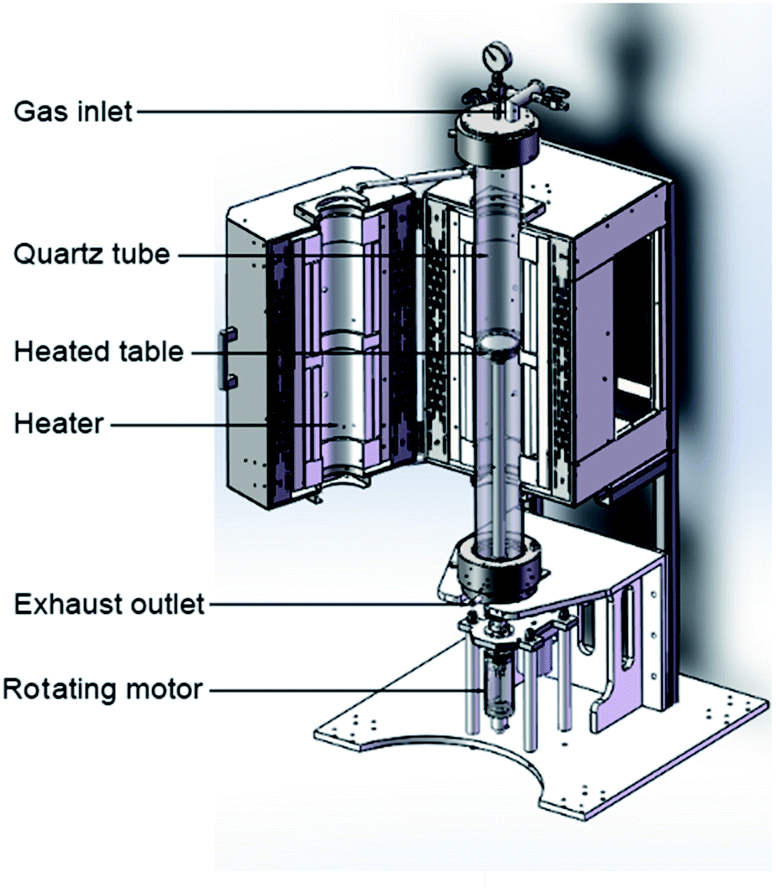 | ||
| Fig. 1 Schematic diagram of a homemade sensitization setup. | ||
| Sample | Atmosphere | Resistance, MΩ | D* (λp, 750, 1), cm Hz1/2 W−1 |
|---|---|---|---|
| 1 | As-grown | 0.02 | — |
| 2 | N2 | 0.05 | — |
| 3 | O2 | 0.1 | — |
| 4 | N2 & I2 | 12 | 1.0 × 10¹⁰ |
| 5 | O2 & I2 | 17 | 2.8 × 10¹⁰ |
2.2 Measurement methods
The phase and crystal structure of films were examined by X-ray diffraction (XRD) with Cu radiation (XRD-6100). SU8020 model Field emission scanning electron microscope (FESEM) with energy dispersive X-ray spectrometer (EDS) was used to observe the morphological evolution. EGK Hall effect measurement system and thermal probe method were used to measure the conductivity type of as-grown and sensitized PbSe films.The detectivity was measured using a SR830 DSP lock-in amplifier and collimated black body at 500 K at room temperature (300 K) with under 750 Hz chopping frequency modulation. The devices were biased at 50 V mm−1 using Agilent E3612A source, with a load resistor matched to the detector resistance. The distance between the blackbody and the detectors was 20 cm.
3. Results and discussion
The XRD patterns were used to reveal the crystal phase evolution of PbSe films in different sensitization atmospheres, as shown in Fig. 2. Only PbSe peaks corresponding to (111), (200) and (220) planes were observed at 25.5°, 29.5° and 41.8° from as-grown films shown in Fig. 2(a), indicating a high purity of CBD-PbSe films. Suffering O2 sensitization, three small peaks at 26.1°, 26.9° and 28.1° could be identified in Fig. 2(c), which corresponds respectively to the (−111), (110) and (002) planes of PbSeO3 phase. The presence of PbSeO3 phase can be described by the eqn (1):| 2PbSe + 3O2 = SeO2(↑) + PbSeO3 + PbO | (1) |
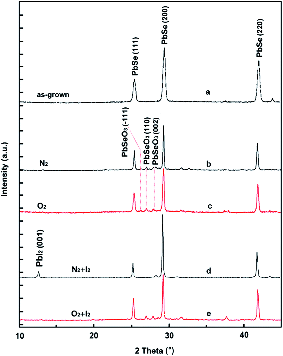 | ||
| Fig. 2 XRD patterns of PbSe films. (a) As-grown, and sensitized at (b) pure N2, (c) pure O2, (d) N2/I2, and (e) O2/I2. | ||
This consists with the previous results.23 It should be noted that PbSeO3 peaks are apparent at the XRD patterns of the PbSe film sensitized in pure N2 atmosphere, as showing in Fig. 2(b). This results from the oxygen absorbed on the surface of as-grown PbSe film. After introducing I2 into O2 at 380 °C for 30 min, besides peaks of PbSeO3 (110) and (002) at 26.9 °and 28.1°, a new weak peak at 12.6° of PbI2 is visible as shown in Fig. 2(e). The equation for the appearance of PbI2 is as follows:
| 2PbSe + 2I2 = 2PbI2 + 2Se(↑) | (2) |
However, the XRD spectrum of the film sensitized under N2 and I2 for 30 min is different from sample sensitized at O2/I2. All peaks associated to PbSeO3 disappears, and the peak at 12.6°, which represents to the (001) of PbI2 is survived. The disappear of PbSeO3 indicates a chemical reaction occurred between PbSeO3 and I2. It could be in accordance with the following reaction (3):
| 2PbSeO3 + 2I2 = 2SeO2(↑) + 2PbI2 + O2(↑) | (3) |
A similar phenomenon was reported.14,15 It suggests that the PbSeO3 was transformed to the PbI2 during iodination stage.
The microstructural evolution under different sensitization atmospheres were shown in Fig. 3. It is obvious from Fig. 3(a) that the as-grown film consists of congregating cubic-shaped PbSe microcrystals of about 0.5 μm edge length. According to the high peak in 29.5° in XRD pattern shown in Fig. 2(a), it corresponds the (200) facet of PbSe and means the majority of pyramidal-shape micro-polycrystalline grow along [111] direction. Moreover, the large microcrystals are assembled by a mass of small nanocrystals, considered as the essential microstructure for infrared response.26 This structure is the result of the cooperative effect of initial Ion-by-Ion (IBI) growth model and later Oriented-Attachment (OA) growth model. The FESEM image of sample sensitized in pure N2 is shown in Fig. 3(b). The average size of PbSe microcrystals has increased as a result of aggregation of small microcrystals with same orientation after 420 °C sensitization.16 At the same time, the grain surface becomes smoother due to recrystallization process. A thin layer over on PbSe film surface could be observed from N2 sensitized PbSe films in Fig. 2(b) marking with red dish line. According to the XRD pattern shown in Fig. 2(b), the phase composition of the top layer should be PbSeO3. After introducing I2 gas, it is found that large recrystallized microcrystals are fragmented into smaller grains as shown in Fig. 3(c). Clearly, an iodinated layer generated also could be observed from the top of PbSe films. Based on our XRD pattern as shown in Fig. 2(e), the top layer is identified as PbI2. This is further confirmed by its cross-section EDS spectrum showing in Fig. 4(b).
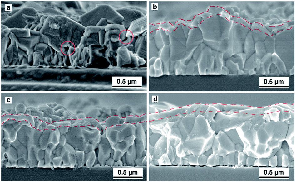 | ||
| Fig. 3 FESEM images of PbSe films. (a) The as-grown film and the film sensitized in (b) N2, (c) N2/I2 and (d) O2/I2. | ||
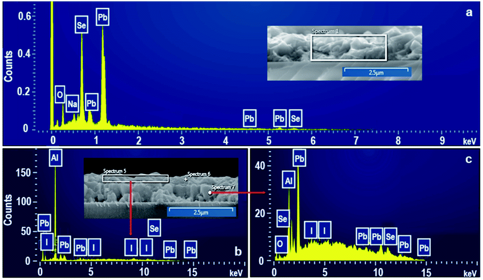 | ||
| Fig. 4 EDS spectra of the PbSe films. (a) As-grown and (b) top-layer and (c) bottom layer of sensitized PbSe film under N2/I2 atmosphere. | ||
However, Moon-Hyung Jang reported that another iodine compound PbSe1−xIx can be identified by their research.24 After sensitized in O2/I2, a typical two-layer structure is also obtained in Fig. 3(d). Our previous research displayed that the top layer formed in O2/I2 sensitization process consists poly-crystalline and nano-crystalline involving Pb–Se–O–I phase.25 The bottom layer is large PbSe crystalline layer, as shown in Fig. 3(d). Note that there is forming nano-crystalline interfaces between large PbSe crystalline grains, which means PbSe crystalline grains immerses in the three-dimensional (3D) network constructed by Pb–Se–O–I nano-crystalline phase.25
EDS was used to identify the constituent elements in top and bottom layers formed in N2/I2 atmosphere, as shown in Fig. 4. Besides of Pb and Se peaks as are expected, oxygen peak presents in the EDS spectra of as-grown CBD PbSe films in Fig. 4(a). There is no Pb–O or Pb–Se–O phases in Fig. 2(a), indicating the present of O peak is attributed to the absorbed O2 in the surface of PbSe film and the holes formed between PbSe crystalline grains, as marked in Fig. 2(a). It is the absorbed oxygen that results in the appearance of Pb–Se–O phase in O2-free N2 sensitization process. Only Pb and I peaks were detected in the EDS spectrum of top layer of PbSe films sensitized at N2/I2 atmosphere in Fig. 4(b). The quantitative EDS analysis reveals that the atomic ratio of I/Pb is 0.57:0.46. However, the EDS spectrum of the bottom layer showing in Fig. 4(c) illuminates displays Pb, Se, I and O peaks. Base on the composite phases and morphology of N2/I2 sensitized PbSe film showing in Fig. 2(d) and 3(d), the bottom layer should be PbSe crystalline layer. At the same time, the presence of I element implies the PbI2 phase are formed in the bottom PbSe crystalline layer. By analogy with O2/I2 sensitized PbSe films,25 obviously, PbI2 phase should mainly distribute in interface of PbSe crystalline grains, then forming a 3D continuous interlocking network, which is key importance for inducing IR-response.
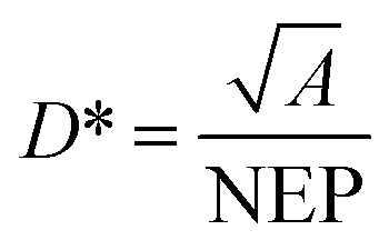
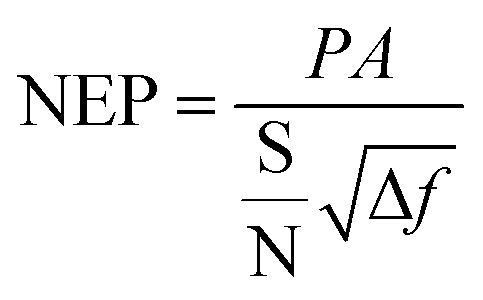
The detectivity of detectors was calculated by the equation:
where S is signal output, N is noise output, and Δf is noise bandwidth (1 Hz). P is incident energy, which can be calculated by following equation:
where α is modulation factor of chopper, σ is Stefan–Boltzmann constant, T is temperature of blackbody, T0 is room temperature, A0 is aperture area of black body and L is distance between blackbody and detectors. In our detection system the value of α is 0.45, T is 500 K, T0 is 300 K, A0 is 0.0127 cm2 and L is 20 cm.
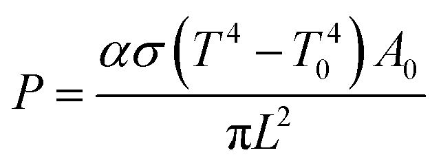
Table 1 summarizes photoelectric detection performance of as-grown and sensitized PbSe infrared photoconductive detectors.
No photo-response was detected for as-grown and sensitized PbSe films without iodine. However, a typical detectivity of 1 × 1010 cm Hz1/2 W−1 was obtained from N2/I2 sensitized PbSe film, indicating that the IR-response triggered from sensitization is not directly relevant to O element or PbSeO3, due to no composition PbSeO3 in N2/I2 sensitized PbSe film. In respect to no-response for pure-N2 sensitized PbSe, it convincingly demonstrates that iodine plays a key role in trigging the infrared response of PbSe films rather than oxygen.
The various resistances of PbSe detectors sensitized in various atmospheres gives a clue about the role of sensitization. As-grown PbSe film by CBD shows p-type with a resistance of about 20 kΩ. The resistance increases to 50 and 100 kΩ suffering from N2 and O2 sensitization respectively, regardless of the sensitization time from 1 to 3 h. Based on the composites phase and morphologies, the increase of resistance is attributed to the forming of high-resistance p-type PbSeO3 around PbSe microcrystal boundaries under O2 atmosphere. After intruding I2, the resistance of PbSe detectors significantly increase to 12–20 MΩ, and O2/I2 sensitized PbSe detector shows a higher resistance than the resistance of PbSe in N2/I2 at the same sensitization time. It is obvious that iodide such as PbI2 play important role in the drastic increase of resistance and the improvement of infrared response. Iodide can serve as a donor and provides electrons. Jang et al. reported electrons from iodide layer will diffuse into PbSe then recombine with holes, which results an abrupt decrease of holes concentration.24 So that the dark resistance of PbSe films increase significantly after iodine treatment.
To confirm the effect of PbI2 in sensitization process under N2/I2 atmosphere, the dependence of N2/I2 sensitization time on the resistance has been studied, as shown in Fig. 5. The result shows the resistance of PbSe films has increased to 41 MΩ significantly as the sensitization was extended to 60 min, companying with the film color change from dark gray to yellow-gray. Further increasing the time to 90 min, the film turns into yellow color and shows a very high resistance. Its XRD pattern shows the PbSe peaks vanish completely, supplemented by a strong PbI2 peak at 12.76°. The conversion from PbSe to PbI2 by over-sensitization subsequently results in a complete disappearance of PbSe IR-response.
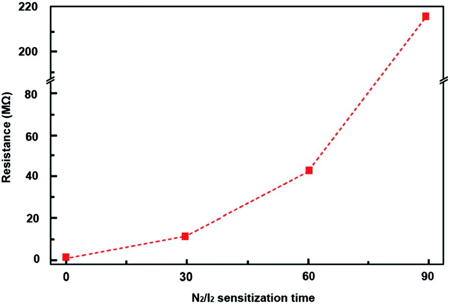 | ||
| Fig. 5 The dependence of N2/I2 sensitization on the resistance of PbSe detectors. | ||
Based on the composite phases, microstructural evolution and resistance change, a new model of the N2/I2 sensitization is proposed, illustrating in Fig. 6. To clearly explain the changes of internal details of the film at various sensitization stages, the as-grown PbSe film is designed to consist of two layers PbSe microcrystals as shown in Fig. 6(a). In the initial stage of sensitization, a PbI2 layer is formed on the surface of PbSe film in Fig. 6(b). With the proceeding of sensitization, iodide will diffuse along the boundaries of PbSe grains into interior of PbSe films, and form 3D PbI2 network structures around large PbSe crystalline grains. The interweave degree of 3D PbI2 network structure is dominated by sensitization time, as shown in Fig. 6(b)–(d). For a short period of sensitization, only tiny amounts of PbI2 is formed, distributing around shallow boundaries of PbSe crystalline grains. The PbI2 level in the films is insufficient to build a continuous 3D network interweaving structure, as shown in Fig. 6(b). With increasing the sensitization time, the continuity of PbI2 3D network interweaving structure is improved due to the increase of the diffusion depth of iodine, illuminating in Fig. 6(c). At the same time, the formed PbI2 separate layer can't completely block the connection between PbSe grains duo to coarse interfaces between PbSe grains. However, a longer sensitization time (over-sensitization) undoubtedly results in a complete, dense PbI2 3D network structure, meaning all interface between PbSe grains is displaced by PbI2 thick films in Fig. 6(d). Originally interconnected PbSe crystalline grains are completely separated by PbI2 film, resulting in high resistance (200 MΩ).
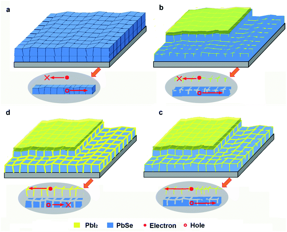 | ||
| Fig. 6 The schematic of the N2/I2 sensitization process and the photo-generated electrons and holes transporting channels at various sensitization time. (a) As-grown, (b) initial, (c) optimized and (d) over sensitization stages. | ||
The PbI2 3D network structure model of N2/I2 sensitization process can offer an explanation for p–n charge separation junction mechanism of PbSe IR detection. In our case, the n-type PbI2 3D network structure distributing in interface of PbSe crystalline grains serves as conducting channels for the photo-generated electrons, the interconnected p-type PbSe grains as the hole conducting channel. Under the bias, photo-generated holes and electrons will transport through p-type PbSe grains and n-type PbI2 3D network conductive channels respectively, resulting an effective separation of electrons and hole, then triggering the IR response. Obviously, there is no any PbI2 distributing in as-grown PbSe films, therefore, no electron conducting channel for transporting the photogenerated electrons, as shown in Fig. 6(a) inset. Although PbI2 3D network is formed at shallow PbSe surface in the initial sensitization stage, there is no continuous 3D PbI2 electron conducting channel forming in the bottom PbSe film, low IR response could be detected, as shown in Fig. 6(b) inset. With iodine deep diffusion along the interface between PbSe grains into the bottom of PbSe film, a continuous, loosen PbI2 3D network is built up throughout the whole PbSe film, severing as photogenerated electron transporting channels under bias. The residual PbSe grains remaining connected each other act as the hole transporting channel under bias, showing in Fig. 6(c) inset. Now, the detectivity of PbSe detector reaches the maximum. After an excessive sensitization process, electrons can transport to the positive electrode along the dense PbI2 3D network conducting channels, but the PbSe hole conducting channels are blocked due to all PbSe grains are separated by 3D PbI2 network, resulting in the disappearance of IR response.
4. Conclusion
We crystalized the controversies about key sensitization element for PbSe sensitization process in this paper. Based on the composite phases, microstructural evolution and resistance change under various sensitization process, a PbI2 3D network transporting model was proposed to clarify the charge separation mechanism of PbSe photoconductive detectors. Acting as the transporting channels for the photogenerated electrons, the integrity and densification of PbI2 3D network structure, which distributes in the interfaces between PbSe crystalline grains, dominates the performances of PbSe detectors. Therefore, the iodine introducing in the sensitization process takes the key role to trigger the infrared response of PbSe films.Conflicts of interest
There are no conflicts to declare.Acknowledgements
This research was funded by the Dalian Science and Technology Innovation Fund (2020JJ26GX022) and Fundamental Research Funds for the Central Universities (Grant No. DUT19RC(3)032).Notes and references
- G. Vergara, R. Linares-Herrero, R. Gutiérrez-Álvarez, M. T. Montojo, C. Fernández-Montojo, A. Baldasano-Ramírez and G. Fernández-Berzosa, VPD PbSe technology fills the existing gap in uncooled low-cost and fast IR imagers, presented in part at the Infrared Technology and Applications XXXVII, 2011, p. 80121Q, DOI:10.1117/12.884018.
- T. H. Johnson, Lead Salt Detectors and Arrays PBS and PbSe, Proc. SPIE, 1983, 443, 60 CrossRef CAS.
- Y. Yasuoka and M. Wada, Thermally Stimulated Current of Vacuum Deposited PbSe Films, Jpn. J. Appl. Phys., 1974, 13(11), 1797–1803 CrossRef CAS.
- F. Briones, D. Golmayo and C. Ortiz, The role of oxygen in the sensitization of photoconductive PbSe films, Thin Solid Films, 1981, 78, 385 CrossRef CAS.
- R. M. Candea, R. Turcu, G. Borodi and I. Beatu, Effects of thermal annealing in air on VE, COD and CAD PbSe films, Phys. Status Solidi A, 1987, 100, 149–155 CrossRef CAS.
- A. Muñoz, J. Meléndez, M. C. Torquemada, M. T. Rodrigo, J. Cebrián, A. J. de Castro, J. Meneses, M. Ugarte, F. López, G. Vergara, J. L. Hernández, J. M. Martín, L. Adell and M. T. Montojo, PbSe photodetector arrays for IR sensors, Thin Solid Films, 1998, 317(1–2), 425–428 CrossRef.
- F. Zhao, S. Mukherjee, J. Ma, D. Li, S. L. Elizondo and Z. Shi, Influence of oxygen passivation on optical properties of pbse thin films, Appl. Phys. Lett., 2008, 92, 211110 CrossRef.
- J. N. Humphrey and R. L. Petritz, Photoconductivity of Lead Selenide – Theory of the Mechanism of Sensitization, Phys. Rev., 1957, 105, 1736–1740 CrossRef CAS.
- J. C. Slater, Barrier Theory of the Photoconductivity of Lead Sulfide, Phys. Rev., 1956, 103, 1631–1644 CrossRef CAS.
- R. L. Petritz, Theory of Photoconductivity in Semiconductor Films, Phys. Rev., 1956, 104, 1508–1516 CrossRef CAS.
- H. Yang, X. J. Li, G. D. Wang and J. B. Zheng, Lead Selenide Polycrystalline Coatings Sensitized Using Diffusion and Ion Beam Methods for Uncooled Mid-Infrared Photodetection, Coatings, 2018, 8, 444 CrossRef.
- H. Yang, X. J. Li, G. D. Wang and J. B. Zheng, The electrical properties of carrier transport between lead selenide polycrystallites manipulated by iodine concentration, AIP Adv., 2018, 8, 085316 CrossRef.
- M. C. Torquemada, M. T. Rodrigo, G. Vergara, F. J. Sanchez, R. Almazan, M. Verdu, P. Rodriguez, V. Villamayor, L. J. Gomez, M. T. Montojo and A. Munoz, Role of halogens in the mechanism of sensitization of uncooled PbSe infrared photodetectors, J. Appl. Phys., 2003, 93, 1778–1784 CrossRef CAS.
- Y. J. Suh and S. H. Suh, Effect of iodine doping in the deposition solution and iodine vapor pressure in the sensitization treatment on the properties of PbSe films, Opt. Eng., 2017, 56, 091607 CrossRef.
- Y. J. Suh and S. H. Suh, Effect of iodine pressure in the sensitization treatment on the structural and electrical properties of PbSe films, Proc. SPIE, Infrared Sensors, Devices, and Applications VI, 2016, vol. 9974, p. 997405 Search PubMed.
- J. J. Qiu, B. B. Weng, Z. J. Yuan and Z. S. Shi, Study of sensitization process on mid-infrared uncooled PbSe photoconductive detectors leads to high detectivity, J. Appl. Phys., 2013, 113, 103102 CrossRef.
- L. H. Zhao, J. J. Qiu, B. B. Weng, C. Chang, Z. J. Yuan and Z. S. Shi, Understanding sensitization behavior of lead selenide photoconductive detectors by charge separation model, J. Appl. Phys., 2014, 115, 084502 CrossRef.
- M. H. Jang, P. M. Litwin, S. S. Yoo, S. J. McDonnell, N. K. Dhar and M. C. Gupta, Mid-wavelength infrared photo response and band alignment for sensitized PbSe thin films, J. Appl. Phys., 2019, 126, 105701 CrossRef.
- S. Ganguly, X. Tang, S. S. Yoo, P. Guyot-Sionnest and A. W. Ghosh, Extrinsic voltage control of effective carrier lifetime in polycrystalline PbSe mid-wave IR photodetectors for increased detectivity, AIP Adv., 2020, 10, 095117 CrossRef CAS.
- M. H. Jang, S. S. Yoo, M. T. Kramer, N. K. Dhar and M. C. Gupta, Electrical transport properties of sensitized PbSe thin films for IR imaging sensors, Semicond. Sci. Technol., 2019, 34, 065009 CrossRef CAS.
- S. Ganguly, M. H. Jang, Y. H. Tan, S. S. Yoo, M. C. Gupta and A. W. Ghosh, A multiscale materials-to-systems modeling of polycrystalline PbSe photodetectors, J. Appl. Phys., 2019, 126, 143103 CrossRef.
- M. C. Gupta, J. T. Harrison and M. T. Islam, Photoconductive PbSe Thin Films for Mid-Infrared Imaging, Mater. Adv., 2021, 2, 3133 RSC.
- M. H. Jang, S. S. Yoo, M. T. Kramer, N. K. Dhar and M. C. Gupta, Properties of chemical bath deposited and sensitized PbSe thin films for IR detection, Semicond. Sci. Technol., 2019, 34, 115010 CrossRef CAS.
- M. H. Jang, E. R. Hoglund, P. M. Litwin, S. S. Yoo, S. J. McDonnell, J. M. Howe and M. C. Gupta, Photoconductive mechanism of IR-sensitive iodized PbSe thin films via strong hole–phonon interaction and minority carrier diffusion, Appl. Opt., 2020, 59, 10228 CrossRef PubMed.
- P. Kumar, M. Pfeffer, E. Schweda, O. Eibl, J. J. Qiu and Z. S. Shi, PbSe mid-IR photoconductive thin films (part I): Phase analysis of the functional layer, J. Alloys Compd., 2017, 724, 316–326 CrossRef CAS.
- J. J. Qiu, Y. Liu, G. D. Zhang, K. H. Shi, Y. Z. Li and Y. M. Luo, Modified Vapor Phase Deposition Technology for High-performance Uncooled MIR PbSe Detectors, RSC Adv., 2021, 11, 34908–34914 RSC.
| This journal is © The Royal Society of Chemistry 2021 |