
 Open Access Article
 This Open Access Article is licensed under a Creative Commons Attribution-Non Commercial 3.0 Unported Licence
An artificial synaptic transistor using an α-In2Se3 van der Waals ferroelectric channel for pattern recognition†
Neha Mohta *,
Ankit Rao,
Nayana Remesh,
R. Muralidharan and
Digbijoy N. Nath*
*,
Ankit Rao,
Nayana Remesh,
R. Muralidharan and
Digbijoy N. Nath*
Centre for Nano Science and Engineering (CeNSE), Indian Institute of Science, Bangalore 560012, India. E-mail: neham@iisc.ac.in; digbijoy@iisc.ac.in
First published on 17th November 2021
Abstract
Despite being widely investigated for their memristive behavior, ferroelectrics are barely studied as channel materials in field-effect transistor (FET) configurations. In this work, we use multilayer α-In2Se3 to realize a ferroelectric channel semiconductor FET, i.e., FeS-FET, whose gate-triggered and polarization-induced resistive switching is then exploited to mimic an artificial synapse. The FeS-FET exhibits key signatures of a synapse such as excitatory and inhibitory postsynaptic current, potentiation/depression, and paired pulsed facilitation. Multiple stable conductance states obtained by tuning the device are then used as synaptic weights to demonstrate pattern recognition by invoking a hidden layer perceptron model. Detailed artificial neural network (ANN) simulations are performed on binary scale MNIST data digits, invoking 784 input (28 × 28 pixels) and 10 output neurons which are used in the training of 42![[thin space (1/6-em)]](https://www.rsc.org/images/entities/char_2009.gif) 000 MNIST data digits. By updating the synaptic weights with conductance weight values on 18000 digits, we achieved a successful recognition rate of 93% on the testing data. Introduction of 0.10 variance of noise pixels results in an accuracy of more than 70% showing the strong fault-tolerant nature of the conductance states. These synaptic functionalities, learning rules, and device to system-level simulation results based on α-In2Se3 could facilitate the development of more complex neuromorphic hardware systems based on FeS-FETs.
000 MNIST data digits. By updating the synaptic weights with conductance weight values on 18000 digits, we achieved a successful recognition rate of 93% on the testing data. Introduction of 0.10 variance of noise pixels results in an accuracy of more than 70% showing the strong fault-tolerant nature of the conductance states. These synaptic functionalities, learning rules, and device to system-level simulation results based on α-In2Se3 could facilitate the development of more complex neuromorphic hardware systems based on FeS-FETs.
Introduction
Advancements in neuromorphic computing techniques in conjunction with brain-inspired hardware platforms are leading to an emergence of next-generation energy-efficient computing systems which can potentially outperform conventional von Neumann computers.1,2 Solid-state devices that mimic the biological synapse and neurons have been attracting interest3–5 in building Artificial Neural Networks (ANN) towards efficient and adaptive implementation of cognitive tasks like classification, speech, and pattern recognition. The basic principle in such tasks is based on weight optimization associated with the individual neurons to achieve excellent efficiencies in supervised learnings.6 For an artificial synaptic device to be effectively used in an ANN, it is desirable that it includes linearly spaced conductance weight states, high endurance, longer retention and low energy consumption. To date, multiple device concepts have been proposed to realize artificial synapse, such as resistive random access memristors (RRAMs),7,8 phase-change memory (PCM),9 charge trapping transistors,10 ion movement in electrolytes,11 and ferroelectric based devices with excellent performance and high integration capability. However, solid state devices are far from even remotely reaching the performance of actual biological synapse. For example, the random switching mechanism in RRAMs and phase-change memory PCM suffer from a significant variation in conductivities due to high cycle to cycle variation. Traditional charge-based memories use a charge trapping layer within a transistor configuration that requires a relatively high operating voltage, high thermal budget and suffers from a non-linear weight update. Electrolyte-gate transistors (EGTs),12 exhibit better weight updating performance thanks to their gate modulation, yet they are not compatible with CMOS technology due to the liquid electrolyte-gate or organic channel material involved.In this context, ferroelectric materials have emerged as a promising candidate for enabling synaptic devices as they lead to fast operation,13 nondestructive readout,14 low-power, low variations, and high on/off ratios.15–17 The partial polarization switching behaviors of the ferroelectric material maybe exploited to emulate the biological synaptic functions by gradually modulating the channel conductance through an external electrical field.
In recent years there have been various studies using ferroelectric material such as PbZr0.2Ti0.8O3 (PZT),18 Hf0.5Zr0.5O2,19 CuInP2S6 (ref. 20) for different device designs such as capacitors, ferroelectric tunnel junctions (FTJ), and ferroelectric field-effect transistors (FeFETs).21 However, among all the reported studies, ferroelectric materials have been studied primarily in metal–semiconductor–metal geometry or as a dielectric layer in a transistor to modulate channel conductance. For example, Zheng et al. chose PbZr0.2Ti0.8O3 (PZT) as a thick (100 nm) ferroelectric gate dielectric, demonstrating the polarization switching albeit at a high operating voltage (∼10 V). Wang et al., have shown a fully organic electrochemical synapse using a ferroelectric dielectric for sensory memory system but is limited by stability issues being organic material.22 Considering the synaptic properties by HfO2 based films are demonstrated at much lower thicknesses and operating voltages, these are limited by difficulty in fabricating and decrease in residual polarization with cumulative switching cycles, resulting in memory with limited endurance.
However, ferroelectrics as a channel material in a FET configuration for mimicking the synapse are barely reported.23,24 FeS-FET, or ferroelectric semiconductor FET25 uses a ferroelectric material as the transistor channel, and is expected to offer more operational freedom to tune conductivity through partial polarization switching at much lower thicknesses. If the ferroelectric channel material happens to be a layered 2D semiconductor, the promises for superior and/or novel functionalities are expected to multiply. This is because layered 2D materials enable aggressive atomic-layer scaling, ultralow power consumption and provide unique advantage: these can be transferred on almost any platform via weak van der Waals bonding which circumvents lattice mismatch issues in traditional heterostructures. This opens up the possibility of realizing heterogenous integration toward system scaling. Devices based on layered 2D semiconductors have been extensively studied toward achieving synaptic functionalities as well as demonstrating cognitive tasks.
In this context, a 2D ferroelectric semiconductor such as indium selenide (In2Se3) would provide an opportunity to exploit properties of both 2D and ferroelectric materials and could offer exciting avenues into neuromorphic hardware platforms.26–29 Unlike traditional insulating ferroelectrics, In2Se3 is a semiconductor with a direct bandgap of about 1.36 eV, making it attractive for conventional electronic and optoelectronic applications also.
In this work, we use multilayer α-In2Se3 as a channel material for FeS-FET with Ta2O5 as a back-gated high-k dielectric. First, we demonstrate the memristive switching of In2Se3-based FeS-FET by exploiting the polarization switching in the material via the gate terminal. The use of high-k dielectric (ε = 15) allows us to work at much lower operating voltages.30 The devices can emulate various characteristics of an artificial synapse such as excitatory and inhibitory postsynaptic current (PSC), paired pulse facilitation/depression (PPF/PPD), and long-term potentiation/depression (LTP/LTD). We have also explored the continuous wight modulation through partial polarization of the channel displaying an excellent linear weight update trajectory with multiple stable conductance states. Finally, leveraging this device-level emulation of synaptic dynamics, the recorded data from a single device is converted to conductance weights for pattern recognition tasks. We achieved an accuracy of 93% using grayscale MNIST (Modified National Institute of Standards and Technology) datasets. This demonstration of ferroelectric channel transistors with synaptic functionalities and subsequent deployment in pattern recognition is expected to open new vistas in hardware neural networks using layered 2D ferroelectrics.
Material characterization
Indium selenide (In2Se3) is known to exist in 5 different phases (α, β, γ, δ, and κ), which are formed by different arrangements of indium and selenium atoms within a single layer.31 For this study, we have used α-In2Se3, which is known to be ferroelectric at room temperature. A high-resolution transmission electron microscopy (HRTEM) imaging of α-In2Se3 was carried out to study its crystal structure (see ESI Note 1† for sample preparation). Fig. 1(a) shows the top view HRTEM image of the few-layered exfoliated α-In2Se3, the staggered atomic arrangement of the structural layer can be attributed to the multi-layered structure, which can be confirmed from the thickness contrast at multiple areas. The inset to Fig. 1(a) shows the FFT pattern of the highlighted area. The lattice parameter calculated is 0.36 nm, which confirms a hexagonal structure for α-In2Se3. Fig. 1(b) shows the enlarged image of the lattice fringes from Fig. 1(a); the high contrast of indium atoms depicts the hexagonal structure. Fig. 1(c) shows the selected area diffraction pattern of the sample. Fig. 1(d) shows the typical Raman spectra of a multi-layered α-In2Se3 flake used in this study, which shows four clear peaks at 89, 105, 180, and 194 cm−1. These peaks correspond to E, A(LO + TO), A(TO), and A(TO) phonon modes, respectively, which are attributed to reported room-temperature ferroelectricity in both out-of-plane (OOP) and in-plane (IP) directions displayed by α-In2Se3.32,33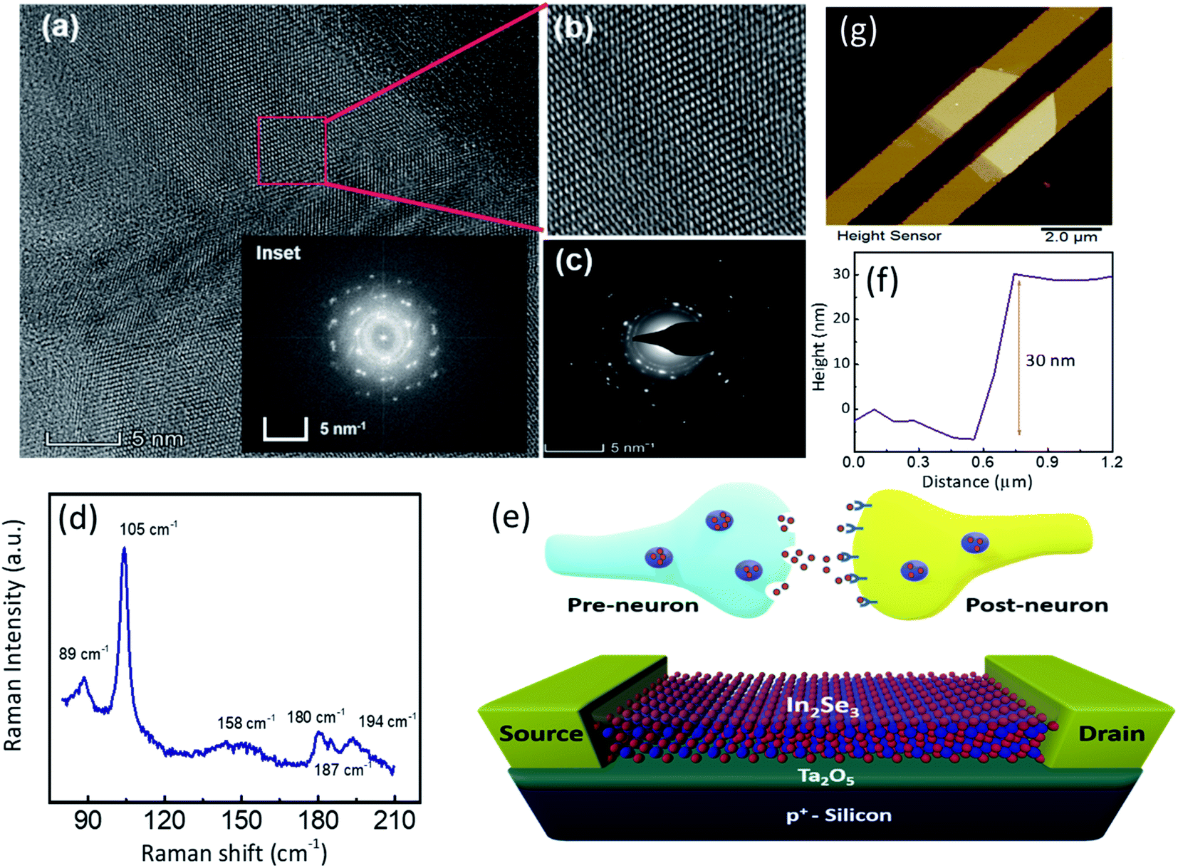 | ||
| Fig. 1 (a) HRTEM image of multi-layered exfoliated α-In2Se3. The inset shows the FFT image of the selected region enlarged in (b). (c) Selected Area Diffraction Pattern (SADP) of the sample. (d) Raman Spectra of α-In2Se3 measured at room temperature. (e) Schematic structure of α-In2Se3 synaptic transistor with 50 nm Ta2O5 and 10 nm Al2O3 as a capping layer with source and drain terminal acting as pre and post neuron respectively as shown in the cartoon (f) The thickness of the flake measured using AFM (g) Atomic Force Microscopy (AFM) scan of the α-In2Se3 based synaptic transistor. | ||
Fabrication and experimental details
Fig. 1(e) shows the schematic of a FeS-FET used in this study where the gate and drain electrodes act as pre and postsynaptic terminals, respectively. 40 nm of Ta2O5 dielectric film is deposited by magnetron sputtering on p+ doped-Si substrate. Multilayer In2Se3 flakes were exfoliated by using a conventional scotch tape approach from a bulk In2Se3 crystal (bought from HQ graphene). Fig. 1(f) shows the AFM height scan of one such flake used for device fabrication. E-beam lithography was used to pattern source-drain contact fingers of Ni/Au (50/70 nm) while the channel length and width in the α-In2Se3 flake were defined 2 μm and 4 μm, respectively. 20 nm of e-beam evaporated Al2O3 was used as a capping layer to encapsulate the device. Fig. 1(g) shows an AFM scan of the final processed device.Result and discussion
When measured for the lateral 2-terminal and 3-terminal electrical characteristics, the α-In2Se3 devices exhibit clear hysteresis, indicative of polarization due to ferroelectricity. Fig. 2(a) shows the output electrical characteristics of a representative FET with the gate floating, exhibiting significant hysteresis in both forward and reverse biases. The direction of hysteresis is anticlockwise from high resistive state (HRS) to low resistive state (LRS). As indicated by the direction of the arrow for a positive voltage sweep from 0 to Vmax and turns to a low resistance state from a sweep voltage of Vmax to 0 V (sweep ii), thus acting as an HRS-LRS (LRS-HRS) memristive device for sweep i (iii) and ii (iv) respectively. The devices produce reproducible hysteresis for different ranges of sweep voltage, a typical characteristic of memristors. The notable asymmetric transport behavior observed in forward and reverse bias can be attributed to the ferroelectric polarization charges that enhance the Schottky barrier of one interface while reducing the barrier of the opposite interface as has been previously reported.33,34 Under the 2-terminal configuration with the gate floating as discussed above, the hysteresis window and the switching ratio is found to gradually increase with an increase in maximum sweep voltage. (ESI Fig. S1†) shows that the switching ratio between HRS to LRS at Vread of −0.5 V approaches 102 as the maximum sweep voltage exceeds 5–6 V. Fig. 2(b) shows the endurance characteristics of the FET that had been switched 100 times between the HRS and the LRS using full-sweep cycles from 0 to ±4 V (please see ESI Fig. S1† for extended data). Fig. 2(c) shows the retention characteristics of FeS-FET at VG = 0 V and VD = 2 V with high (HRS) and low (LRS) stable states. Formation of built-in electric field due to the presence of mobile charges strengthens the polarization of the ferroelectric dipole and improves the endurance. The switching ratio between the LRS and HRS remains one order of magnitude for more then 1100 s showing the substantial endurance of the devices. Fig. 2(d) shows the typical n-type transfer characteristics of the back-gated FeS-FET with drain current of 2 μA μm−1 at a drain bias of Vds = 0.5 V and an on/off ratio of 105. Forward and reverse transfer-curve sweeps evoked typical clockwise hysteresis, which occurs due to the partial polarization switching of the In2Se3 layers (see extended electrical data in ESI Fig. S2†). As previously reported for a back-gated In2Se3 transistor with high dielectric thickness, the vertical electric field is not enough to completely switch the polarization in the In2Se3 channel.25 The mechanism can be understood as follows: when the applied gate voltage is −6 V, positive bound charges get accumulated at the bottom of the α-In2Se3 layer (oxide/semiconductor interface), and negatively bound charges get accumulated at the top layer of the channel. This is known as the polarization downstate as illustrated in Fig. 3(a) with a schematic energy band diagram.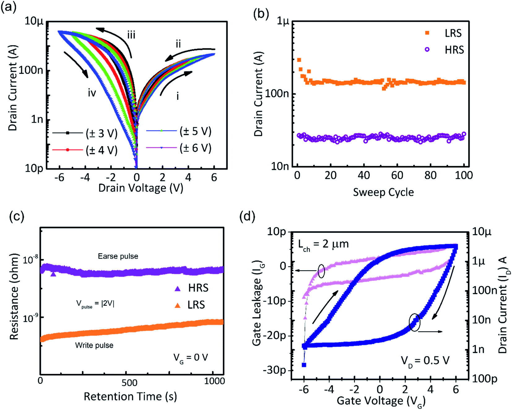 | ||
| Fig. 2 (a) Output characteristics of FeS-FET exhibiting ferroelectric hysteresis with maximum sweep range of VD varying from (−3 V, 3 V) to (−6 V, 6 V). The sweeping directions are indicated by the arrows. (b) Resistance switching between the HRS and LRS over 100 cycles. The amplitude of the write voltage were set at 2 V. (c) Retention test, in which the ratio of the HRS and LRS states remained over one order of magnitude for up to 1100 s. (d) Transfer characteristics and gate leakage of In2Se3 FeS-FET showing on/off current ratio of 105. | ||
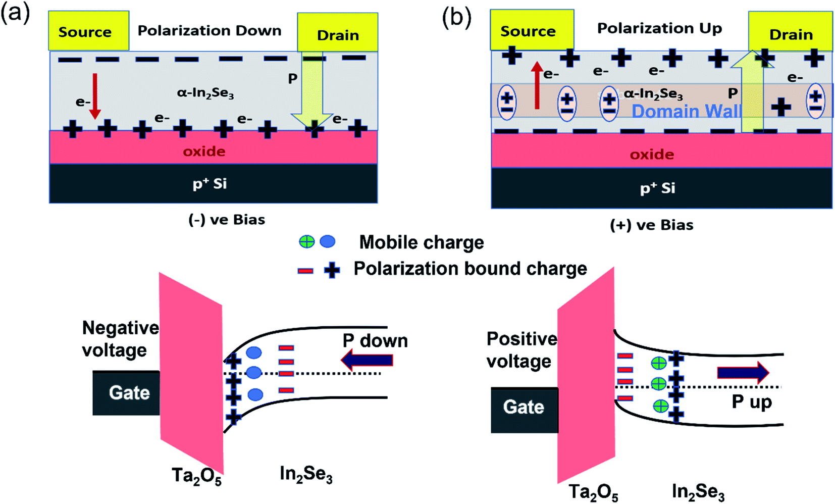 | ||
| Fig. 3 (a and b) Schematics showing the device operation and corresponding band diagrams, of the synaptic transistor explaining clockwise hysteresis loop achieved due to partial polarization switching between multiple layers. | ||
As the gate voltage is swept from −6 V towards positive voltage, the free carriers in the channel cause an increase in electron density in the bottom layer giving rise to an increase in channel conductance. With a further increase in gate voltage, the ferroelectric polarization in the bottom layer starts changing sequentially from downward to upward, but the vertical field is not high enough to flip the polarization of the top layer completely. The top layer remains in a downward polarization state, giving rise to domain walls in the channel. A situation known as partially polarized switching emerges due to this, and it is observed at +6 V in this case. With a further change in the gate voltage, the upward polarization in the bottom layer starts flipping, leading to a decrease in the channel conductance as shown in the band diagram [Fig. 3(b)]. The switching of polarization in our devices is gradual and not abrupt, as observed in other ferroelectric oxide films where the gate oxide (and not the channel) is ferroelectric. Low-temperature measurements were carried out on a representative α-In2Se3 FeS-FET, exhibiting a similar hysteresis window as room temperature. This confirmed that the ferroelectric nature of α-In2Se3 flakes is responsible for the hysteresis instead of charge trapping between the oxide and semiconductor interface. (The details of the measurements are shown in ESI Fig. S3†).
To mimic various synaptic functionalities of the In2Se3 based FeS-FET structure, single and sequentially triggered (or presynaptic) pulses are applied at the gate. The channel conductance increases or decreases depending upon the amplitude and the duration of the applied presynaptic pulse. The conductance of In2Se3 is equivalent to the synaptic weight of the biological synapse, modulated by the gate voltages. When a single negative pulse with an amplitude of −2 V and duration of 40 ms at VD = 0.5 is applied at the gate of the transistor, a typical excitatory postsynaptic current (EPSC) of 20 nA is observed as the channel conductance increases, as shown in Fig. 4(a). Since In2Se3 is an n-type semiconductor, ideally the current should decrease as we apply a negative pulse but the reverse phenomenon is observed. This is due to the coupled IP and OOP ferroelectricity present in In2Se3 layers.33 On the application of a negative pulse, an additional in-plane electric field gets strengthened opposite to the built-in electric field leading to overall change in drain current, thus we observe a positive current for a negative pulse. Also, an inhibitory current (IPSC) of −3 nA is observed corresponding to a positive pulse with an amplitude of 2 V and duration of 40 ms, as shown in Fig. 4(b). The corresponding insets show the EPSC and IPSC responses to the presynaptic pulses of different pulse amplitudes with the same pulse width of 40 ms, showing the increase or decrease in the channel conductivity as a function of the applied pulse amplitude. As the amplitude of the gate voltage pulse increases, the additional electric field inside the In2Se3 starts increasing, providing a higher number of ferroelectric domains switching in the In2Se3 channel layer. Hence, the conductivity of the channel increases or decreases with an increase in the gate bias, as testified by the current values.
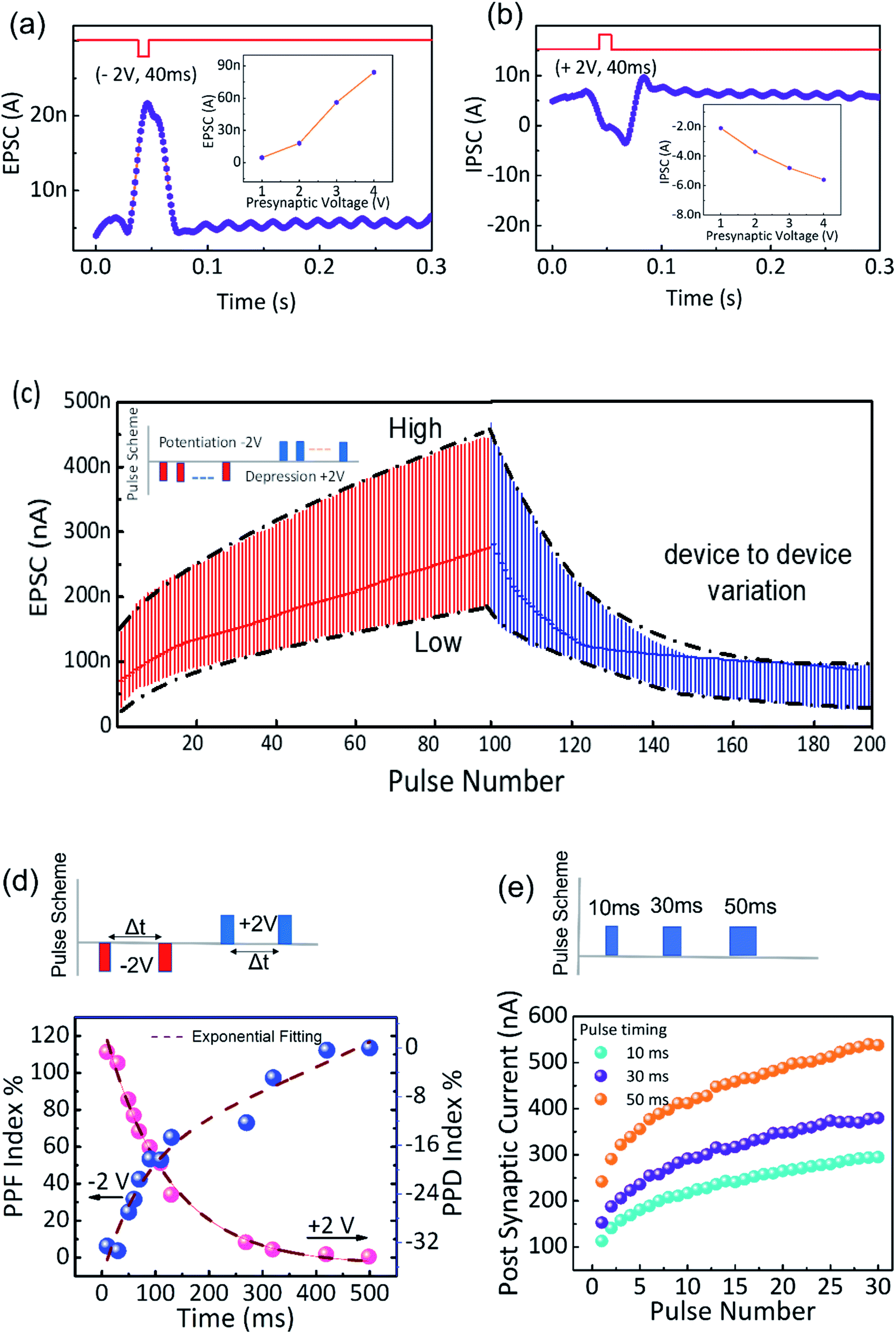 | ||
| Fig. 4 (a) EPSC response to a programming gate pulse of −2 V. (b) IPSC response to an erasing gate pulse of 2 V. The corresponding insets show the EPSC and IPSC response of synaptic transistor at different back-gate voltages ranging from (−4 to +4 V). (c) Potentiation and depression responses of the channel to 100 sequential pulses at VLTP and VLTD of ±2 V and 30 ms for different devices. The upper and lower dashed lines represent the maximum and minimum values of the conductivity, and the solid line represents the average value of the conductance states observed for different devices with minimal variation. (d) Top part shows the pulse scheme applied at the back-gate terminal of the In2Se3 synaptic transistor. PPF index determined by the time interval of two input presynaptic pulses (ΔtPPF = tpre2 − tpre1). Dashed lines indicate the fitting, (e) Sequential 30 excitatory postsynaptic current corresponding to gate pulses of different pulse widths (10 ms 30 ms and 50 ms) at fixed pulse amplitude of 2 V. | ||
Long-term synaptic plasticity, which consists of long-term potentiation (LTP) and long-term depression (LTD) of synaptic weights, is essential to learning and memory functions in human brain.35 Implementation of long-term plasticity is an essential phenomenon for better accuracy and reliability in analyzing various cognitive tasks like pattern and speech recognition. In previous studies, ferroelectric-based memristive devices have demonstrated long-term plasticity by utilizing the dynamic ferroelectric domain evolution and robust domain stability.36,37 In our FeS-FETs, long term potentiation/long-term depression are observed when trains of 100 gate voltage pulses VLTP (−2 V) and VLTD (+2 V), are sequentially applied as shown in Fig. 4(c). Negative pulses triggered at the back gate lead to an increasing polarization switching in the In2Se3 layer, enhancing the channel conductivity with increasing pulse number, which manifests as potentiation. Depression is the opposite of potentiation, and corresponds to a decrease in channel conductivity with increasing pulse number. The upper and lower dashed lines represent the maximum and minimum values of the conductivity, and the solid line represents the average value of the conductance states observed for different devices with minimal variation.
We further confirm the emulation of paired pulse facilitation/depression (PPF/PPD), a characteristic that can be exploited for time-dependent learning algorithms.38 In a biological synapse, the time interval Δt between two successive presynaptic inputs affects the magnitude of the postsynaptic current. This dependence of the change of postsynaptic current on Δt can be captured by measuring the channel current for two gate pulses of the same amplitude separated by different values of Δt (Fig. 4(d)). In our devices, we applied the gate pulses of amplitude −2 V (or +2 V) while the drain bias is 0.1 V. PPF and PPD are quantified in an index called the PPF (or PPD) index, which is defined by the ratio of (E2 − E1)/E1 where E2 and E1 are the channel current values corresponding to the 2nd and the 1st gate pulses respectively. Time constants of 110 ms and 77 ms for depression and facilitation respectively, are estimated based on a double exponential fit to the data points. These characteristic time constants are comparable in scale to those of a biological synapse.
Further, we studied spike rate dependent plasticity (SRDP) i.e.; the impact of the pulse width for 30 sequential excitatory pulses with a fixed pulse amplitude of 2 V, as shown in Fig. 4(e). The postsynaptic current decreases from 250 nA to 100 nA when the gate pulse width is reduced from 50 ms to 10 ms. As the pulse width increases, the In2Se3 layers in the channel get more orderly polarized, resulting in higher current. As a synaptic device, the stability of the device is of critical importance. Thus, the endurance of the devices is examined for multiple, successive potentiation and depression cycles. ESI Fig. S4† shows the endurance characteristics of the FeS-FET for 30 excitatory and inhibitory pulses at ±2 V, 30 ms. No degradation in performance is observed in the devices, as confirmed by the consistent stability exhibited up to 30 cycles. ESI Fig. S4† also shows the endurance for 100 consecutive excitatory and inhibitory pulses for a total of 600 pulses with multiple stable conductance states, demonstrating the robustness of FeS-FET devices for ANN in neuromorphic computing.
Next we studied the performance of our synaptic devices in the implementation of neural networks, i.e., recognition accuracy (pattern recognition) of MNIST data digits. The recognition performance of memristive devices is affected by various parameters such as (a) weight conductance non-linearity (NL), (b) total variation margin (ΔG) in conductance, and (c) conductance weight states (Nstates),39,40 as discussed below.
(a) Weight conductance non-linearity (NL)
The conductance of a synaptic device usually increases steeply for the first few potentiation and depression pulses and then becomes saturated as the number of pulses increases.5,41 Every pulse leads to a different response in terms of weight modulation trajectory, and its cumulative effect does not follow a simple linear relation. This is known as non-linearity (NL). The NL factor is used to analyze its effect on learning efficiency for gradual conductance changes.42 Increasing the NL degrades the recognition accuracy due to the difficulty in the convergence of conductance weight into a stable value; a smaller NL is thus more desirable for better recognition accuracy. ESI Fig. S5† shows the non-linearity observed in LTP and LTD curves for different pulse widths. Our device exhibits good linearity with NL_LTP (0.12, 0.31 and 0.81 for 10 ms 30 ms and 50 ms) respectively, with a near symmetric LTP and LTD curves. The observed values are amongst the lowest reported values using a ferroelectric channel for artificial synapse.(b) Total variation margin (ΔG) in conductance
Another critical factor which affects the accuracy of ANN-based implementation of cognitive tasks such as pattern recognition is ΔG defined by the minimum (Gmin) and maximum (Gmax) conductance weight variation. Previous studies on ΔG have concluded that a more extensive variation margin provides more analog states to store information but at the cost of recognition accuracy, especially for ΔG >20. Thus, it is necessary to optimize the synaptic device specifications for improved system-level performances.40,43 For the FeS-FET synaptic device under study, we observed a total variation margin of 7, 9 and 12 for 10 ms 30 ms and 50 ms respectively, for a hundred sequential excitatory pulses.A comprehensive study of various parameters like timing between two consecutive pulses and pulse amplitude is required to improve the values of non-linearity and variation margin values to study their effect on learning accuracy.
(c) Conductance weight states (Nstates)
In neuromorphic computing, a higher number of conductance weight states guarantees reliability in data retention or endurance.44,45 In this study, we have shown that even 20 conductance weight states are sufficient to provide stable recognition accuracy of 85%. The multiple conductance states in our devices could be attributed to the controlled polarization of individual layers in the semiconducting channel. For the α-In2Se3 FeS-FET under study, ESI Fig. S6† shows more than 64 stable conductance states obtained after applying a hundred excitatory pulses of magnitude 2 V and 10 ms duration. The value of conductance state at each pulse is increasing in linear fashion, with a few conductance states either overlapping or less than the previous pulse value. In order to avoid this overlap, we extracted the stable conductance states by setting threshold value for ΔG. The effective stable conductance states were extracted using (GN − GN−1) conductance weight values when the difference between G1 and G2 exceeds a certain threshold. Here G1 and G2 are conductance weight values from pulse-1 and pulse-2, respectively. A threshold of 0.2%, 0.3% and 0.5% was used to extract the stable weight values from 100 pulses. ESI Fig. S6† shows the extracted values of three different cases, corresponding to Nstates = 10 (case-1), Nstates = 20 (case-2) and Nstates = 64 (case-3), to identify its impact on pattern recognition. It can be seen that our device shows high number of conductance states (>64) with much less non-linearity in LTP confirming potential of our FeS-FET in ANN for future high performance neuromorphic computing.Benchmarking of various synaptic parameters reported in the literature for different synaptic devices vis-à-vis the FeS-FET in this study is made in Table 1.
| Devices | HfAlyOx ReRAM47 | HZO-Si FINFET45 | Charge trapping transistor48 | GrFeFET49 | HfZrOx-FeFET50 | CNT-transistor51 | FeS-FET (this work) |
|---|---|---|---|---|---|---|---|
| Gmax/Gmin | 25 | 4.98 | — | — | 45 | 57 | 12 |
| NL | >5 | 1.58–7.57 | 0.06–0.89 | 2.8 | 1.75–1.46 | 0.82 | 0.1–1.8 |
| Conductance states | ∼25 | >32 | 35 | — | 32 | — | >64 |
| Operating voltage | 2–8 V | 3.2–3.7 V | 10 V | 16 V | 3.4–3.7 V | 1–5 V | 1–2 V |
| Neural network | 320–3 | 528–250–125–10 | 400–100–10 | 1000–100–10 | 400–100–10 | 784–10 | 784–256–10 |
| Number of layers | 2 | 3 | 2 |
2 | >2 | 2 | 2 |
| Total training data | Yale face database | 100000 MNIST |
60000 MNIST |
60000 MNIST |
100000 MNIST |
60000 MNIST |
60000 MNIST |
| Energy consumption | 30 nJ | 12.1 pJ | — | 50 nJ | — | 10 nJ | 10 pJ |
| Recognition accuracy | ∼0.90 | 0.8 | 0.87 | 0.94 | 0.9 | 0.7 | 0.93 |
In this study, we have investigated the impact of Nstates of the α-In2Se3 synaptic device to assess its applicability to pattern recognition of the system. We present detailed artificial neural network (ANN) simulations performed on the Modified National Institute of Standard and Technology (MNIST) database to demonstrate neuromorphic computing. Here, we categorize 28 × 28 pixels of the MNIST dataset using a single-layer perceptron model, performing supervised learning. As explained in Fig. 5(a), the 784 input neurons (X1 to X784) correspond to 28 × 28 pixels of an original image, and the 10 output neurons relate to 10 classes of digits (Z0 to Z9). During the simulation, 42000 patterns were used as a training dataset, and 18000 images were used to test the recognition accuracy of each epoch/training cycle. As illustrated in flowchart Fig. 5(b), every training cycle is divided into two halves, i.e., forward propagation and backward propagation. During forward propagation, each neuron in the input layer receives a value corresponding to a pixel in the image and is assigned to an input vector (Xi), which is then transformed into 256 hidden layer neurons through a weight matrix (Wi,j) and further down to 10 output neurons (Zi,k) through output layer weight matrix (Vj,k). The summation of weights and input vector are converted to output vector by a sigmoid activation function. Next, during backward propagation, we fine-tune the weights (Wi,j, Vj,k) based on the difference between the output value and the label value. The trained input (Wi,j) and output (Vj,k) weight values obtained after reaching maximum efficiency are then replaced by synaptic conductance weight values (Nstates) of the FeS-FET under study. ESI Fig. S5† shows the learning accuracy using the different number of middle layer neurons. The higher the number of neurons, the higher the accuracy achieved. Using 256 middle neurons, a linear transformation of the device conductance values is performed so that the conductance range is consistent with the weight range using the following relation46
| Cj = AIj + B | (1) |
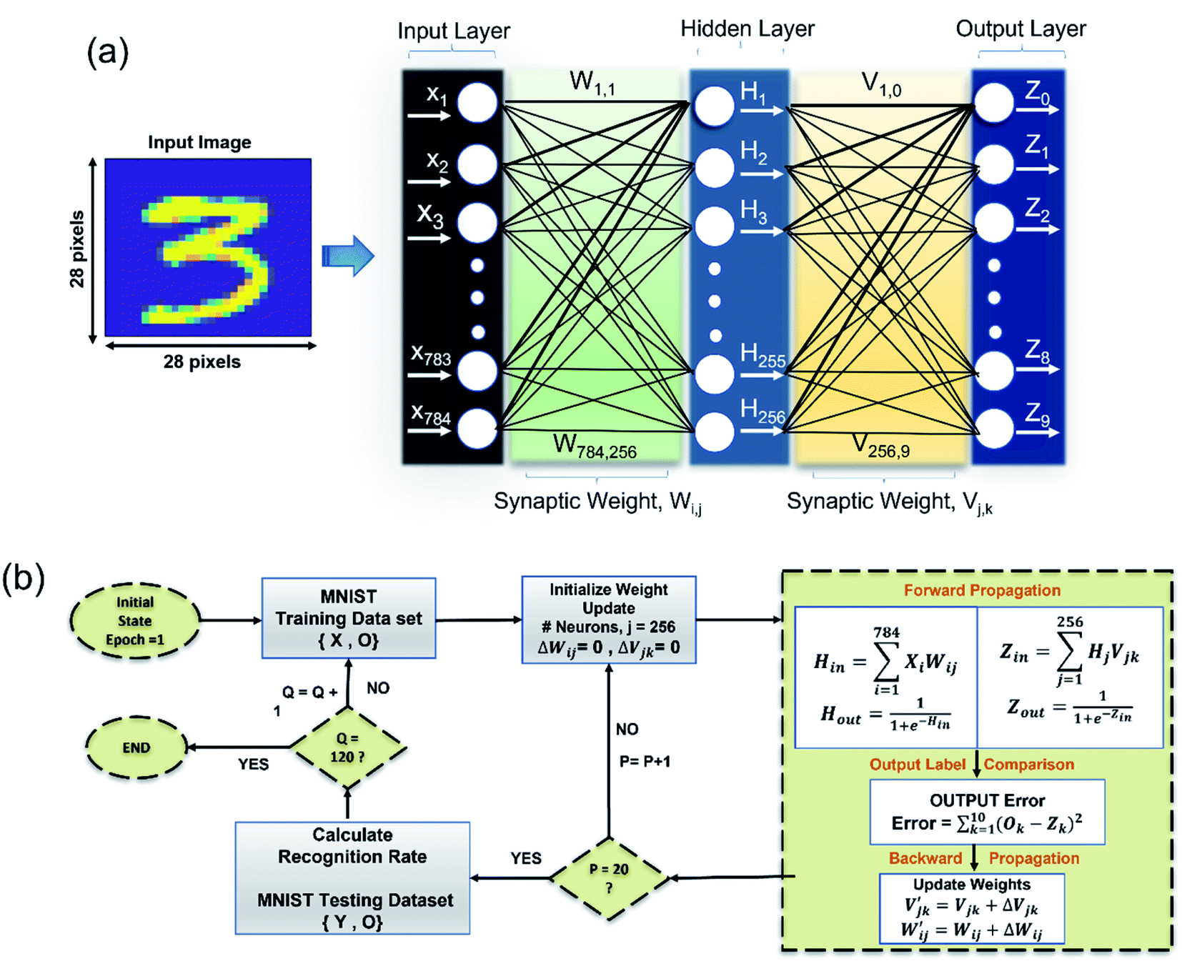 | ||
| Fig. 5 (a) Artificial neural network comprises of three layers, containing 783 input neurons, 256 middle (hidden) layer neurons, and 10 output neurons. (b) Flowchart of the training recognition cycle, where N represents the total number of training images, i is in the range 1–784 input neuron, j is in the range 30–256 hidden layer neuron, k is in the range 1–10 output neuron, and these indices imply the sequence number of the input neurons, middle (hidden) layer neurons and output results, respectively. | ||
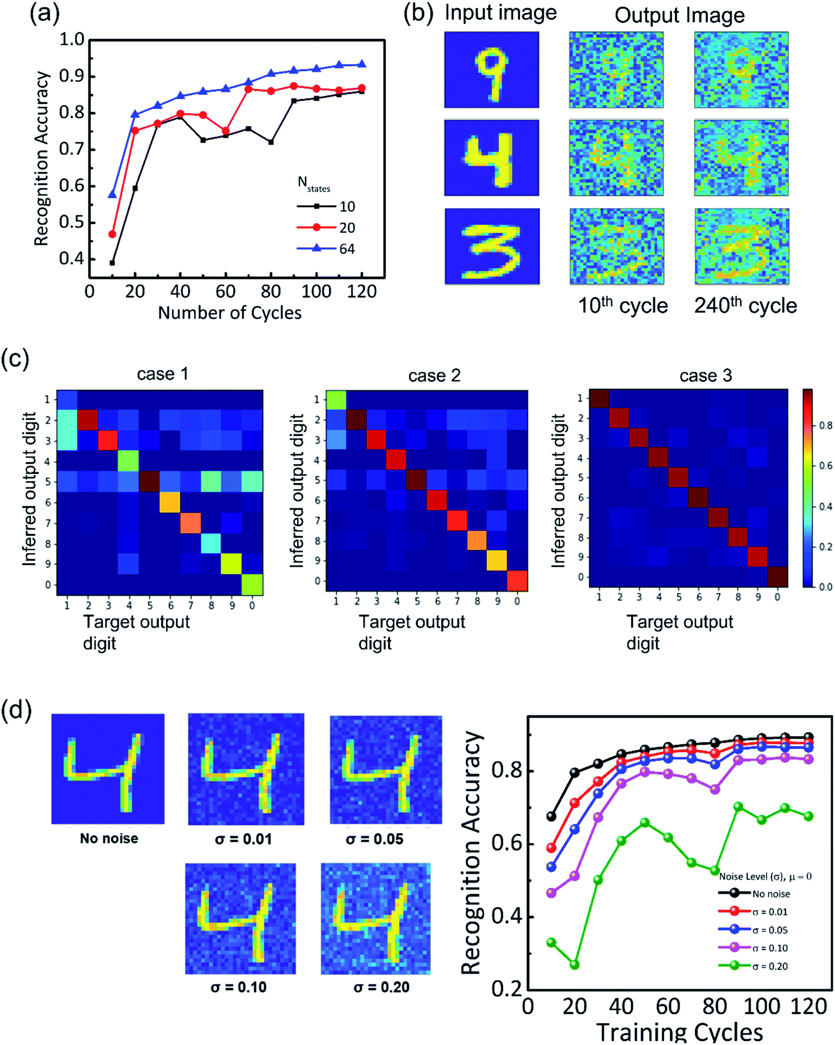 | ||
| Fig. 6 (a) Recognition accuracy as a function of the training cycle for different Nstates (10, 20, and 64). (b) Weight mapping images after 10th and 240th training cycles. (c) Average confusion matrix of the testing data set for 18000 MNIST data. The digits highlighted in dark color represents the number of identified digits for all three cases, whereas those with lighter color code shows the confusion between two digits, for example digit 2, 3 for case 1. (d) Recognition accuracy as a function of the training cycle for different noise pixels introduced in the test data. Numerical digit 4 represents different % of variance introduced as background noise pixels for calculating the classification accuracy. Introducing background noise leads to difficulty in convergence state of conductance weight value. | ||
Next, we studied the average confusion/error created by the proposed algorithm for different conductance weight values. Fig. 6(c) shows the average confusion matrix over the 10 digits of the MNIST test data for all three cases. Given the recognition accuracy was 75% for case-1 and 85% for case-2, most of the input digits were identified correctly in both the cases, with the most common confusions for digits 2, 3, and 5 being higher for case-1 compared to case-2. It was found that case-3 corresponding to Nstates = 64 exhibited less confusion in precisely identifying the input digits than the other two cases.
Besides this, we studied the learning accuracy with 64 conductance weight states by introducing noise to the background pixels. Gaussian noise with mean μ = 0 and variance σ = 0.01, 0.05, 0.10, 0.20 is introduced to the background pixels to check the stability of the weight states (Fig. 6(d)). More than 70% accuracy is achieved for a variance value of 0.10, which indicates that the conductance weight states hold great potential in the classification of the digits. This establishes the fault tolerance nature of the α-In2Se3 FeS-FET. The accuracy can be further improved by increasing the training cycles but at the cost of higher energy consumption involved in simulations.
Further, the energy efficiency of the proposed FeS-FET based synaptic device is evaluated. The energy consumption per pulse is governed using the following relation: E = I × V × t, where (V) indicates the programming voltage, (I) the channel current, and (t) the pulse width. The energy consumption per switching of the device can be lowered significantly by reducing the pulse width. The smallest value is estimated to be 10 pJ ∼ (1 V, 10 ms), which is lower than that of graphene/Fe-FET (∼50 nJ)49 and can be further decreased by decreasing the pulse widths to an even lower value. The learning accuracy of FeS-FET synapse is benchmarked against other ReRAM, FINFeT, Fe-FET and charge trapping transistors in Table 1. FeS-FETs exhibit a clear accuracy advantage compared to other ReRAM and charge trapping transistor synapses. The high recognition accuracy (93%) results from a low non-linearity factor, reasonable ΔG variation and high number of conductance states. The low non-linearity (0.12) values can be attributed to ordered partial polarization switching mechanism in different layers of In2Se3 thus providing higher number of conductance weight states compared to ReRAM and FiNFET. The fabricated FeFET synapse exhibits (>64) analog states that can be modulated symmetrically (potentiation and depression) using applied electric field, whereas in charge trapping transistors, there is a linear increase in conductance weights for initial spikes which gets saturated as the number of pulse increases. The ΔG values extracted for different pulse schemes are compared with other reported values in Table 1. The required variation margin should be higher than 10 to achieve accuracies of >80%.8 Compared to (ref. 48), we achieved 85% accuracy with as low as 20 conductance states providing a reasonable balance between accuracy and variation margin (ΔG ∼9). It should be noted that it is unclear what NL and ΔG values are appropriate for the reliable operation of a neuromorphic system. In other words, an investigation on the impact of high/low NL and ΔG is necessary, as is particularly evident when investigating the effect on the pattern recognition accuracy. Though the recognition accuracy observed for graphene based FeFET is higher then our FeS-FET, but they are operated at much higher voltages (16 V) providing a disadvantage when using for neuromorphic computing systems.
Nevertheless, the results presented here highlight the potential of using In2Se3 based FeS-FET based non-volatile synaptic transitor for training of neural network that outperforms other devices in terms of non-linearity (0.12–1.8), high number of conductance states (>64), desirable ΔG, low energy consumption (10 pJ) and electric-field controlled switching.
Conclusion
In summary, we fabricated and demonstrated synaptic devices that use multilayer ferroelectric α-In2Se3 as the channel in a back-gated FET configuration with Ta2O5 as the dielectric. Devices exhibited excellent nonvolatile resistance switching modulated by source-drain voltage (Vds) and back-gate voltage (VG), allowing it to be used as both memristors as well as a synaptic device. The gradual change in conductivity of the channel through partial polarization switching between the In2Se3 layers is an important step for studying the adaptive learning in ANNs. The potentiation and depression properties in FeS-FET were measured by applying incremental excitatory and inhibitory bias pulses that exhibit excellent weight-update properties, with nonlinearity as low as 0.12, appropriate variation margin (ΔG = 7–12) a low energy consumption of 10 pJ per spike and a large number of stable conductance states(>64). Leveraging these synaptic parameters, an artificial neural network was simulated corresponding to different Nstates (10, 20 and 64) that showed 93% recognition accuracy in recognizing handwritten digits from the MNIST database. Introduction of a noise (variance value of 0.10 in) in background pixels showed accuracy of more than 70% indicating strong fault-tolerant nature of the conductance states. Using 2D α-In2Se3 as a ferroelectric channel in synaptic transistor has shown high performance in stable conduction states, low power consumption of 10 pJ per spike, and high endurance. These synaptic functionalities, learning rules and device to system-level simulation results based on α-In2Se3 are expected to facilitate the development of more complex neuromorphic hardware systems based on FeS-FETs.Characterization techniques
All the electrical characteristics of the FeS-FET were measured under ambient conditions and room temperature using a probe station (Agilent B1500 Semiconductor Parameter Analyzer). Presynaptic spikes were applied on the back-gate electrodes, and postsynaptic current output was measured by applying a voltage (Vds = 0.10 V) between the source and drain electrodes. The thickness of Ta2O5 was measured by spectroscopic ellipsometer (M-2000, J.A. Woollam). The structural properties of the α-In2Se3 flake were measured using FEI TEM Themis (60–300). The thickness of flake was measured in tapping-mode using Bruker Scanasyst atomic Force Microscopy. All ANN simulations were performed using MATLAB and Python.Conflicts of interest
The authors declare no competing financial interest.Acknowledgements
We acknowledge funding support from MHRD through NIEIN project, from MeitY and DST through NNetRA. We also acknowledge funding from MHRD, MeitY and DST Nano Mission for supporting the facilities at CeNSE. The authors thank the staff and facility technologists of the Micro and Nano Characterization Facility (MNCF) and the National Nano Fabrication Facility (NNFC).References
- C. K. Machens, Building the human brain, Science, 2012, 338(6111), 1156–1157, DOI:10.1126/science.1231865.
- M. W. Cole, D. S. Bassett, J. D. Power, T. S. Braver and S. E. Petersen, Intrinsic and task-evoked network architectures of the human brain, Neuron, 2014, 83(1), 238–251, DOI:10.1016/j.neuron.2014.05.014.
- Y. Park and J. S. Lee, Artificial Synapses with Short- and Long-Term Memory for Spiking Neural Networks Based on Renewable Materials, ACS Nano, 2017, 11(9), 8962–8969, DOI:10.1021/acsnano.7b03347.
- Z. Cheng, C. Ríos, W. H. P. Pernice, C. David Wright and H. Bhaskaran, On-chip photonic synapse, Sci. Adv., 2017, 3(9), 2–7, DOI:10.1126/sciadv.1700160.
- L. Wang, et al., Artificial Synapses Based on Multiterminal Memtransistors for Neuromorphic Application, Adv. Funct. Mater., 2019, 29(25), 1–10, DOI:10.1002/adfm.201901106.
- J. Yang, Y. Zhao, J. C. W. Chan and C. Yi, Hyperspectral image classification using two-channel deep convolutional neural network, IEEE International Geoscience and Remote Sensing Symposium (IGARSS), 2016, pp. 5079–5082, DOI:10.1109/IGARSS.2016.7730324.
- H. J. Song, J. B. Wang, X. L. Zhong, J. J. Cheng and G. K. Zhong, Large resistive switching in Pt/BNT/HfO2/Pt capacitors, RSC Adv., 2014, 4(92), 50891–50896, 10.1039/c4ra07400a.
- M. Prezioso, F. Merrikh-Bayat, B. D. Hoskins, G. C. Adam, K. K. Likharev and D. B. Strukov, Training and operation of an integrated neuromorphic network based on metal-oxide memristors, Nature, 2015, 521(7550), 61–64, DOI:10.1038/nature14441.
- H. S. P. Wong, et al., Phase change memory, Proceedings of the IEEE, 2010, 98(12), 2201–2227, DOI:10.1109/JPROC.2010.2070050.
- S. Rehman, et al., Neuro-transistor based on uv-treated charge trapping in mote2 for artificial synaptic features, Nanomaterials, 2020, 10(12), 1–11, DOI:10.3390/nano10122326.
- S. Desbief, et al., Electrolyte-gated organic synapse transistor interfaced with neurons, Org. Electron., 2016, 38, 21–28, DOI:10.1016/j.orgel.2016.07.028.
- J. Wang, Y. Li, C. Yin, Y. Yang and T. L. Ren, Long-term depression mimicked in an IGZO-based synaptic transistor, IEEE Electron Device Lett., 2017, 38(2), 191–194, DOI:10.1109/LED.2016.2639539.
- S. Dünkel, et al., A FeFET based super-low-power ultra-fast embedded NVM technology for 22nm FDSOI and beyond, Tech. Dig. - Int. Electron Devices Meet., 2018, 19.7.1–19.7.4, DOI:10.1109/IEDM.2017.8268425.
- W. Chung, M. Si, P. R. Shrestha, J. P. Campbell, K. P. Cheung and P. D. Ye, First direct experimental studies of Hf0.5Zr0.5O2 ferroelectric polarization switching down to 100-picosecond in Sub-60mV/dec germanium ferroelectric nanowire FETs, IEEE xplore Dig. Tech. Pap. - Symp. VLSI Technol., 2018, pp. 89–90, DOI:10.1109/VLSIT.2018.8510652.
- D. D. Lu, S. De, M. A. Baig, B. Qiu and Y. Lee, A computationally efficient compact model for ferroelectric FETs for the simulation of online training of neural networks, Semicond. Sci. Technol., 2020, 35(9), 095007 CrossRef CAS.
- Y. Nishitani, Y. Kaneko, M. Ueda, T. Morie and E. Fujii, Three-terminal ferroelectric synapse device with concurrent learning function for artificial neural networks, J. Appl. Phys., 2012, 111(12), 1–7, DOI:10.1063/1.4729915.
- S. Moon, J. Shin and C. Shin, Understanding of polarization-induced threshold voltage shift in ferroelectric-gated field effect transistor for neuromorphic applications, Electron, 2020, 9(5) DOI:10.3390/electronics9050704.
- Z. D. Luo, X. Xia, M. M. Yang, N. R. Wilson, A. Gruverman and M. Alexe, Artificial Optoelectronic Synapses Based on Ferroelectric Field-Effect Enabled 2D Transition Metal Dichalcogenide Memristive Transistors, ACS Nano, 2020, 14(1), 746–754, DOI:10.1021/acsnano.9b07687.
- L. Chen, et al., Ultra-low power Hf0.5Zr0.5O2 based ferroelectric tunnel junction synapses for hardware neural network applications, Nanoscale, 2018, 10(33), 15826–15833, 10.1039/c8nr04734k.
- M. Si, P. Y. Liao, G. Qiu, Y. Duan and P. D. Ye, Ferroelectric Field-Effect Transistors Based on MoS2 and CuInP2S6 Two-Dimensional van der Waals Heterostructure, ACS Nano, 2018, 12(7), 6700–6705, DOI:10.1021/acsnano.8b01810.
- D. J. Kim, et al., Ferroelectric tunnel memristor, Nano Lett., 2012, 12(11), 5697–5702, DOI:10.1021/nl302912t.
- H. Wang, et al., A Ferroelectric/Electrochemical Modulated Organic Synapse for Ultraflexible, Artificial Visual-Perception System, Adv. Mater., 2018, 30(46), 1–9, DOI:10.1002/adma.201803961.
- B. Tang, et al., Novel Type of Synaptic Transistors Based on a Ferroelectric Semiconductor Channel, ACS Appl. Mater. Interfaces, 2020, 12(22), 24920–24928, DOI:10.1021/acsami.9b23595.
- Y. Zhao, D. Yu, Z. Liu, S. Li and Z. He, Memtransistors Based on Non-Layered In2S3 Two-Dimensional Thin Films with Optical-Modulated Multilevel Resistance States and Gate-Tunable Artificial Synaptic Plasticity, IEEE Access, 2020, 8, 106726–106734, DOI:10.1109/ACCESS.2020.3000589.
- M. Si, et al., A ferroelectric semiconductor field-effect transistor, Nat. Electron., 2019, 2(12), 580–586, DOI:10.1038/s41928-019-0338-7.
- N. Divya Bharathi and K. Sivasankaran, Research progress and challenges of two dimensional MoS2 field effect transistors, J. Semicond., 2018, 39(10) DOI:10.1088/1674-4926/39/10/104002.
- M. Donnelly, D. Mao, J. Park and G. Xu, Graphene field-effect transistors: The road to bioelectronics, J. Phys. D: Appl. Phys., 2018, 51, 49, DOI:10.1088/1361-6463/aadcca.
- A. K. Sood, et al., Review of Graphene Technology and Its Applications for Electronic Devices, in Graphene - New Trends and Developments, InTech, 2015, p. 38, vol. i Search PubMed.
- E. Singh, P. Singh, K. S. Kim, G. Y. Yeom and H. S. Nalwa, Flexible Molybdenum Disulfide (MoS2) Atomic Layers for Wearable Electronics and Optoelectronics, ACS Appl. Mater. Interfaces, 2019, 11(12), 11061–11105, DOI:10.1021/acsami.8b19859.
- N. Mohta, R. K. Mech, S. Sanjay, R. Muralidharan and D. N. Nath, Artificial Synapse Based on Back-Gated MoS2 Field-Effect Transistor with High-k Ta2O5 Dielectrics, Phys. Status Solidi A, 2020, 217(19), 1–6, DOI:10.1002/pssa.202000254.
- F. Xue, et al., Room-Temperature Ferroelectricity in Hexagonally Layered α-In2Se3 Nanoflakes down to the Monolayer Limit, Adv. Funct. Mater., 2018, 28(50), 1–7, DOI:10.1002/adfm.201803738.
- F. Xue, et al., Gate-Tunable and Multidirection-Switchable Memristive Phenomena in a Van Der Waals Ferroelectric, Adv. Mater., 2019, 31(29), 1–9, DOI:10.1002/adma.201901300.
- C. Cui, et al., Intercorrelated In-Plane and Out-of-Plane Ferroelectricity in Ultrathin Two-Dimensional Layered Semiconductor In2Se3, Nano Lett., 2018, 18(2), 1253–1258, DOI:10.1021/acs.nanolett.7b04852.
- P. Hou, et al., Resistive switching behavior in α-In2Se3 nanoflakes modulated by ferroelectric polarization and interface defects, RSC Adv., 2019, 9(52), 30565–30569, 10.1039/c9ra06566k.
- G. Bi and M. Poo, Synaptic Modifications in Cultured Hippocampal Neurons : Dependence on Spike Timing, Synaptic Strength, and Postsynaptic Cell Type, J. Neurosci., 1998, 18(24), 10464–10472 CrossRef CAS PubMed.
- S. Oh, H. Hwang and I. K. Yoo, Ferroelectric materials for neuromorphic computing, APL Mater., 2019, 7(9) DOI:10.1063/1.5108562.
- Y. Nishitani, Y. Kaneko, M. Ueda, E. Fujii and A. Tsujimura, Dynamic observation of brain-like learning in a ferroelectric synapse device, Jpn. J. Appl. Phys., 2013, 52(4) DOI:10.7567/JJAP.52.04CE06.
- G. Q. Bi and M. M. Poo, Synaptic modifications in cultured hippocampal neurons: Dependence on spike timing, synaptic strength, and postsynaptic cell type, J. Neurosci., 1998, 18(24), 10464–10472, DOI:10.1523/jneurosci.18-24-10464.1998.
- S. Lim, et al., Adaptive learning rule for hardware-based deep neural networks using electronic synapse devices, Neural Computing and Applications, 2019, 31(11), 8101–8116, DOI:10.1007/s00521-018-3659-y.
- S. Kim, M. Lim, Y. Kim, H. D. Kim and S. J. Choi, Impact of Synaptic Device Variations on Pattern Recognition Accuracy in a Hardware Neural Network, Sci. Rep., 2018, 8(1), 1–7, DOI:10.1038/s41598-018-21057-x.
- T. Paul, T. Ahmed, K. Kanhaiya Tiwari, C. Singh Thakur and A. Ghosh, A high-performance MoS 2 synaptic device with floating gate engineering for neuromorphic computing, 2D Mater, 2019, 6(4), 045008, DOI:10.1088/2053-1583/ab23ba.
- G. W. Burr, et al., Experimental Demonstration and Tolerating of a Large-Scale Neural Network (165 000 Synapses) Using Phase-Change Memory as the Synaptic Weight Element, IEEE Trans. Electron Devices, 2015, 62(11), 3498–3507, DOI:10.1109/TED.2015.2439635.
- S. Kim, et al., Pattern Recognition Using Carbon Nanotube Synaptic Transistors with an Adjustable Weight Update Protocol, ACS Nano, 2017, 11(3), 2814–2822, DOI:10.1021/acsnano.6b07894.
- W. Kim, A. Chattopadhyay, A. Siemon, E. Linn, R. Waser and V. Rana, Multistate Memristive Tantalum Oxide Devices for Ternary Arithmetic, Sci. Rep., 2016, 6, 1–9, DOI:10.1038/srep36652.
- A. Prakash, J. Park, J. Song, J. Woo, E. J. Cha and H. Hwang, Demonstration of low power 3-bit multilevel cell characteristics in a TaOx-Based RRAM by stack engineering, IEEE Electron Device Lett., 2015, 36(1), 32–34, DOI:10.1109/LED.2014.2375200.
- Z. H. Fan, et al., ReS2 Charge Trapping Synaptic Device for Face Recognition Application, Nanoscale Res. Lett., 2020, 15(1), 1–8, DOI:10.1186/s11671-019-3238-x.
- P. Yao, et al., Face classification using electronic synapses, Nat. Commun., 2017, 8, 1–8, DOI:10.1038/ncomms15199.
- Y. C. Chou, C. W. Tsai, C. Y. Yi, W. H. Chung, S. Y. Wang and C. H. Chien, Neuro-Inspired-in-Memory Computing Using Charge-Trapping MemTransistor on Germanium as Synaptic Device, IEEE Trans. Electron Devices, 2020, 67(9), 3605–3609, DOI:10.1109/TED.2020.3008887.
- Y. Chen, et al., Graphene–ferroelectric transistors as complementary synapses for supervised learning in spiking neural network, npj 2D Mater. Appl., 2019, 3(1), 1–9, DOI:10.1038/s41699-019-0114-6.
- S. Oh, et al., HfZrOx-based ferroelectric synapse device with 32 levels of conductance states for neuromorphic applications, IEEE Electron Device Lett., 2017, 38(6), 732–735, DOI:10.1109/LED.2017.2698083.
- A. M. Shen, C. L. Chen, K. Kim, B. Cho, A. Tudor and Y. Chen, Analog neuromorphic module based on carbon nanotube synapses, ACS Nano, 2013, 7(7), 6117–6122, DOI:10.1021/nn401946s.
Footnote |
| † Electronic supplementary information (ESI) available: TEM sample preparation method; resistance switching ratio and endurance characteristics for 100 sweep cycles at Vd = −2 V on planar (metal-In2Se3-metal) configuration; ID–VG curve for multiple gate sweep range from (±3 to ±6 V), ID–VD characteristic curve at room temperature; Remnant current as a function of gate voltage sweep from (3 V to 6 V), Coercive VG (at ID = 10 nA μm−1) as a function of maximum sweep VG on the same device; Temperature dependence of the hysteresis loops for planar and FET configuration; nonlinearity (NL) and total variation margin (ΔG) extraction formula for different pulse widths (10 ms, 30 ms and 50 ms); stable conductance states extraction note; linear transfer coefficient ‘A’ and ‘B’ for different conductance states; recognition accuracy for different numbers of hidden neurons (30, 60, 120 and 256) as a function of training cycles; variance introduced as background noise pixels for calculating the classification accuracy. See DOI: 10.1039/d1ra07728g |
| This journal is © The Royal Society of Chemistry 2021 |