
 Open Access Article
 This Open Access Article is licensed under a Creative Commons Attribution-Non Commercial 3.0 Unported Licence
Influence of low-voltage discharge energy on the morphology of carbon nanostructures in induced benzene transformation
Ivan Vasilievich Bodrikova,
Anna Gennadevna Ivanovab,
Alexander Leonidovich Vasilievbcd,
Evgeny Yurievich Titov *a,
Dmitry Yurievich Titova and
Anton Igorevich Serova
*a,
Dmitry Yurievich Titova and
Anton Igorevich Serova
aNizhny Novgorod State Technical University n. a. R. E. Alekseev, Minin St., 24, 603950 Nizhny Novgorod, Russia. E-mail: e.titov@nntu.ru
bShubnikov Institute of Crystallography of FSRC “Crystallography and Photonics” RAS, 59 Leninsky Prospect, 119333 Moscow, Russia
cNational Research Center “Kurchatov Institute”, 1, Akademika Kurchatova Sq., 123182 Moscow, Russia
dMoscow Institute of Physics and Technology, National Research University, Dolgoprudny, Moscow Region, Russia
First published on 10th December 2021
Abstract
The directions of the transformation of benzene induced by low-voltage discharges at various energies of pulsed discharges were revealed. This paper shows the dependencies of the morphology and other characteristics of nanostructures obtained in the induced transformation of benzene on the energy of pulsed discharges. Nanostructures with different morphologies are formed when the energy of the low-voltage discharges changes during the induced transformation of benzene in the liquid phase. Two types of carbon nanostructures were formed in the induced destruction of benzene with a 90 μF capacitor. The first type of structure includes graphite fibers, two- and three-layer graphene sheets, as well as two- and three-layer hollow spheres and microstructures in the form of CNHs. The microstructures of the second type were onion-like spheroids. An increase in the capacitance up to 20![[thin space (1/6-em)]](https://www.rsc.org/images/entities/char_2009.gif) 090 μF led to the formation of two types of nanostructures: onion-like spheroids and carbon fibers. A further increase in the capacitance to 40090 μF caused the formation of onion-like spheroids.
090 μF led to the formation of two types of nanostructures: onion-like spheroids and carbon fibers. A further increase in the capacitance to 40090 μF caused the formation of onion-like spheroids.
1. Introduction
Among the large number of methods for the synthesis of nanosized carbon materials, methods based on the transformation of hydrocarbons by induced non-thermal plasma in a liquid are relatively new. The development of methods for generating plasma in a liquid to stimulate the polycondensation of hydrocarbons in nanostructures began in the 21st century.1–3 In this case, there are several ways to generate plasma in a liquid: microwave discharges,3–6 electric arc discharge in liquids,7–9 electrolysis by plasma glow discharge,10,11 and the interaction of plasma with liquid at atmospheric pressure.12,13 At present, electron beam irradiation (EBI) has been a unique tool for engineering the structures of materials,14–16 and combined methods of ultrasound and electric arc in a liquid are also used to synthesize nanoscale carbon structures.17–19 Depending on the method of generating plasma in a liquid, structures with different morphologies of nanocarbon are obtained: carbon onions,20,21 SWCNHs and CNHs,22–25 CNTs,26–28 single and multilayer graphene layers,29,30 fullerenes,31,32 and other nanostructures. Synthesis under low-temperature plasma conditions was realized using low-intensity process parameters.33,34 Such modes of the process lead to the formation of active particles (electrons, radicals, and ions), which makes it possible to achieve a high conversion of reagents at atmospheric pressure and relatively low temperatures.Low-voltage electric discharges in the liquid phase were used in the developed method of induced benzene destruction. Excitation of organic substances occurs in the interelectrode space when exposed to pulsed streamer discharges with a duration of 0.1–2 ms with electron densities up to 1025 m−3 and gas temperatures of 2000–3250 K, obtained depending on the conditions.35 The method developed by the authors for inducing reactions by low-voltage electric discharges in the liquid phase is used for the synthesis of carbon structures, functional nanomaterials, and the processing of toxic compounds.36–38
Benzene is one of the best precursors for carbon nanostructures because aromatic and polyaromatic molecules are well carbonized.39–41 The process parameters strongly affect the size, structure, and purity of the carbon structures.42,43 Thus, during the pyrolysis of benzene in a quartz reactor at 900 °C, only carbon from the cotton-like soot is formed in the empty zone of the reactor, while the formation of a lamellar structure prevails on the solid surface.
In this work, we investigated the effect of the power of low-voltage electric discharges in the liquid phase on the direction of benzene destruction to obtain carbon nanostructures. The development of methods for generating low-voltage pulsed discharges in liquid media to induce destruction and polycondensation of hydrocarbon fragments is a newly developed principle to stimulate chemical processes. Pulse discharges generated at voltages of 40–80 V have energies of 700–900 kJ mol−1.36 Consequently, the generated energy significantly exceeds the energy required to break the chemical bonds, which produces highly active particles. Furthermore, these particles were “quenched” by the environment. This allows selective “assembly” of intermediates into carbon structures at the stage of relaxation under mild conditions.
2. Experiment
Benzene (≥99.9%, Sigma-Aldrich) was used as the reagent. Fig. 1 shows the setup of the working reactor (made of Teflon, 40 cm3 capacity) used in this study, where graphite electrodes (6 mm diameter) were mounted inside it. A 60 V DC voltage source with a capacitance of 90 μF, 20090 μF, and 40090 μF was used to generate low-voltage discharges by varying the distance between the electrodes. The duration and power of the discharge were controlled using a control unit. A detailed description of the discharge-control unit and impact-energy calculations can be found elsewhere.36,45 Table 1 shows the electric discharge parameters during the destruction of benzene under the action of electric discharges in the liquid phase.
 | ||
| Fig. 1 Scheme of experimental setup R: reactor; RC: reflux condenser; E: electrodes; M: manometer; V: valve; GT: gas trap; C: clutch; SM: stepper motor; D: stepper motor driver; PS: stepper motor power supply; CS: current sensor; MCS: microprocessor control system; VS: voltage source with an internal 90 μF capacitor Cin; Cex is an external variable capacitor. | ||
| Characteristics of electrical discharges | Capacitor capacity, μF | ||
|---|---|---|---|
| 90 | 20 090 | 40 090 | |
| Average pulse duration, ms | 0.2 | 0.9 | 1.3 |
| Average pulse frequency, Hz | 56 | 79 | 86 |
| Average pulse amplitude, A | 31 | 33 | 33 |
| Average pulse energy, J | 0.004 | 0.02 | 0.04 |
To prevent the reactant from evaporating, a reflux condenser was used (maintained at −15°C). The temperature in the reactor did not exceed the boiling point of the reactant. The resulting gas was cooled and trapped in a gas trap. The reactor was set up such that the pressure was almost constant.
Table 2 presents the experimental data on the conversion of benzene and the yield of the products with an experimental time of 30 min.
| Process characteristics | Capacitor capacity, μF | ||
|---|---|---|---|
| 90 | 20090 |
40090 |
|
| Conversion, wt% | 12.2 | 22.2 | 25.1 |
| The output of gaseous products, wt% | 82.6 | 69.7 | 65.2 |
| The yield of solid products, wt% | 17.4 | 30.3 | 34.8 |
| Energy consumption for the synthesis of carbon structures, kW h g−1 | 0.87 | 0.19 | 0.11 |
| Specific surface area of carbon structures, m2 g−1 | 277 | 102 | 133 |
The morphologies and structures of the powders were studied using transmission electron microscopy (TEM), scanning transmission electron microscopy (STEM), electron diffraction (ED), energy-dispersive X-ray (EDX) microanalysis, X-ray diffraction (XRD), scanning electron microscopy (SEM), and energy-dispersive X-ray spectroscopy (EDXS) using a Supra 50VP scanning electron microscope (Carl Zeiss AG, Germany) with an INCA microanalysis system (Oxford Instruments). SEM images were obtained in the secondary electron (SE) mode.
Specimens for TEM, STEM, and EDXS studies were prepared by dipping the Lacey carbon film on the Cu grid into the vail with the powder, and the samples by TEM/STEM/EDX methods were carried out in an Osiris T/SEM (Thermo Fisher Scientific, USA) equipped with a high-angle annular dark-field detector (HAADF) (Fischione, USA) and an X-ray energy dispersive spectrometer Super X (ChemiSTEM, Bruker, USA) at an accelerating voltage of 200 kV.
The determination of the specific surface area of carbon structures was carried out by the Bruner–Emmett–Teller (BET) method. The specific surface area was measured on an Autosorb iQ specific surface area and porosity analyzer (Quantachrome Instruments, USA) as a result of processing the adsorption isotherm of nitrogen vapors at a liquid nitrogen temperature of −196 °C in the range of relative pressures p/p0 from 0.05 to 0.3 by the BET method. Before each measurement, the samples were degassed at a temperature of 300 °C for 4 h under a high vacuum.
The XRD patterns of the samples at 90 μF, 20090 μF, and 40090 μF were recorded using a powder X-ray diffractometer (Rigaku MiniFlex 600, Rigaku, Japan) with CuKα radiation (40 kV, 15 mA, Ni–Kβ-filter) in the angle range of 10° to 50° with a scanning step of 0.02° and a rate of 0.7° min−1. The phases were identified in the PXDRL program (Rigaku, Japan) using the ICDD PDF-2 datasets (release 2020).
The composition of the gas-phase products was determined by GC-FID using a Kristall 5000.2 gas chromatograph.
3. Results and discussion
The surface morphology of the carbon structures obtained at 90 μF (Fig. 2a) is characterized by pointed conical nanostructures 30–50 nm in length and 2–5 nm in average diameter.46 It can be assumed that the pointed nanostructures are closed conical nanotubes or nanofibers. Such nanostructures form aggregates – almost spherical clusters, in the form of peculiar “flowers” or “dahlia buds” the surface morphology of the carbon structures obtained at 20090 and 40090 μF (Fig. 2b and c) is characterized by clusters of nanostructures 10–40 nm range with spherical shapes.
 | ||
| Fig. 2 SE SEM images of the solid products at: 90 μF (a), 20090 μF (b), 40090 μF (c). | ||
Before studying the samples by TEM, including high-resolution (HR) TEM and ED, the elemental composition of the solid products was studied. The results of elemental mapping by EDX microanalysis of benzene polycondensation products with capacitors of 90, 20090, and 40090 μF are shown in Fig. 3. The maps showed a homogeneous distribution of elements, namely carbon and oxygen, throughout the sample. Quantitative EDX analysis showed that the carbon structures obtained at a higher discharge power were characterized by the highest oxygen content. For all regimes, the contents of C and O were nearly the same, namely 98 at% and 2 at%, respectively.
 | ||
| Fig. 3 HAADF STEM images and correspondent EDX elemental mapping of polycondensation of solid products at: 90 μF (a), 20090 μF (b), 40090 μF (c). | ||
The change in the discharge energy had practically no effect on the composition of the gaseous products (Table 3). The main gaseous products of the induced transformation of benzene are hydrogen (77.1–79.4 mol%) and acetylene (18.1–19.6 mol%). In addition to the substances indicated in the table, minor amounts of ethane, propane, and C6+ hydrocarbons were recorded.
| Reaction products | Capacitor capacity, μF | ||
|---|---|---|---|
| 90 | 20090 |
40090 |
|
| H2 | 79.4 | 77.9 | 77.1 |
| C2H2 | 18.1 | 18.8 | 19.6 |
| CH4 | 1.0 | 1.1 | 1.0 |
| C3H4 | 0.9 | 1.1 | 0.9 |
| C2H4 | 0.3 | 0.3 | 0.4 |
| neo-C5H12 | 0.2 | 0.9 | 1.3 |
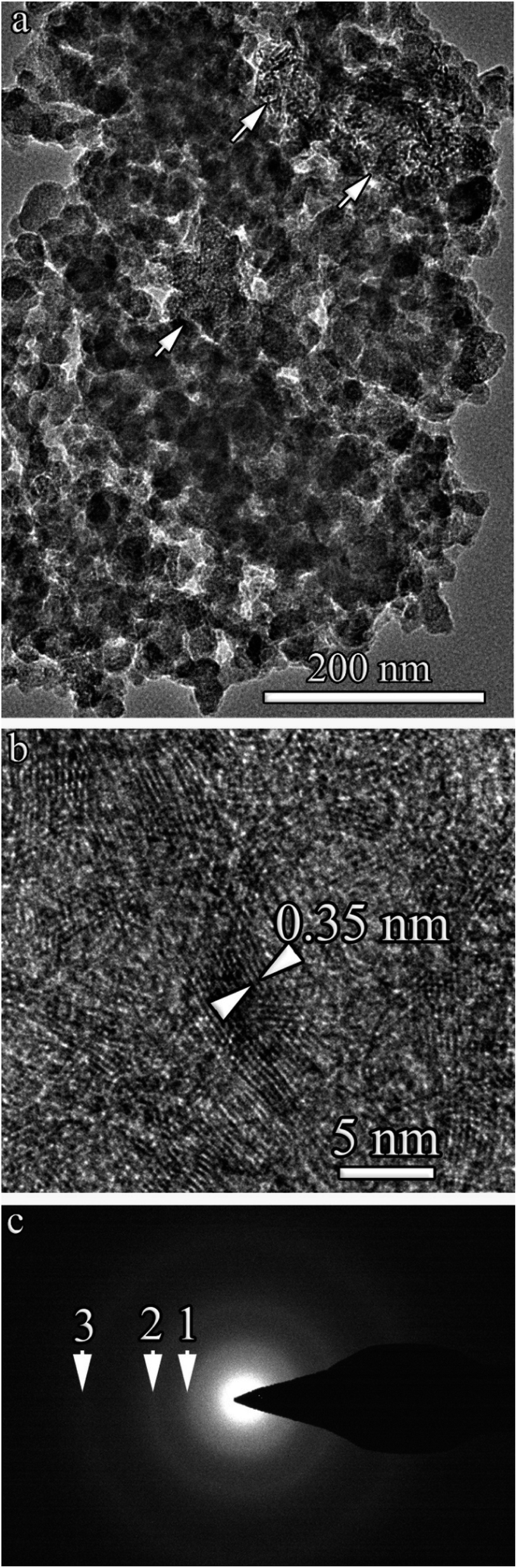
With a capacitance of 90 μF, the destruction of benzene induced by low-voltage discharges led to the formation of two types of carbon materials (Fig. 4). The first type (Fig. 4a) consists of a variety of carbon structures shown in the bright-field (BF) TEM images in Fig. 5 and 6a; the second type is onion-like spheroids (Fig. 4b).
 | ||
| Fig. 4 BF TEM image of 90 μF specimen demonstrating different morphology. (a) – Graphite flakes, two- and three-layered graphene, hollow spheres and (b) onion-like spheroids. | ||
 | ||
| Fig. 5 BF TEM image of graphite flakes. | ||
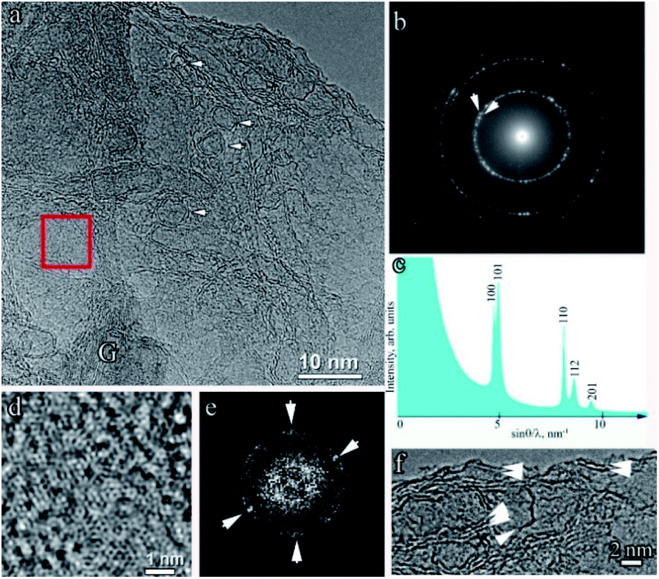 | ||
| Fig. 6 The first type microstructure in the sample 90 μF: (a) BF TEM image of the graphene layers with hollow spheres (arrowed) and the area with graphite (marked by G). (b) The selected area electron diffraction pattern from the area, shown in (a). (c) Histogram of rotationally averaged scattering intensity. (d) Fourier filtered image of the area marked by a red square in (a). (e) Fast Fourier transform pattern from the red square (a) area. (f) The enlarged BF TEM image of the edge of the specimen, shown in (a). The embedded edges of graphene layers are marked by arrows. | ||
The typical structure of the resulting graphite fibers (flakes) is shown in Fig. 5. The length of such fibers in the direction parallel to the (0001) planes can reach 0.15 μm, and the thickness (perpendicular to these planes) is 10–20 nm. The interplanar spacing determined from the HR-TEM images (Fig. 5) was slightly larger than that of hexagonal graphite and was 0.345 nm. It can be assumed that an increase in the interplanar spacing is associated with the high defect structure of the graphene planes in the graphite fibers (flakes). In addition to graphite fibers, in part of the first type sample, two- and three-layer graphene sheets, two- and three-layer spherical hollow structures (hollow spheres) were found (Fig. 6a, f and 7).
 | ||
| Fig. 7 BF TEM image of a CNHs. The double and triple graphene layers are marked by arrows. | ||
The selected area electron diffraction pattern of the sample shown in Fig. 6a is shown in Fig. 6b, and the radius-averaged histogram of scattered electron intensity is shown in Fig. 6c. The interplanar distances correspond to hexagonal (2H) graphite with a space group P63/mmc with unit cell parameters a = 0.2460(2) nm, c = 0.6704(5) nm.47 It can be seen that the most intense peak corresponding to the 002 reflection with a characteristic distance of 0.3352 nm is absent in the electron diffraction pattern. This is due to the high texture of the sample, in which the graphene planes are perpendicular to [001]. The texture also appears in the form of arcs appearing on reflection 101, as indicated by the arrows in Fig. 6b. Reflections 101 appear as a result of diffraction on curved graphene planes, examples of which are shown by arrows in Fig. 6f. The results of filtering the HR-TEM images are shown in Fig. 6d. This image (Fig. 6d) and the two-dimensional Fourier spectrum (Fig. 6f), obtained from the area bounded by the red square (Fig. 6a), unambiguously indicates the high imperfection of the graphene layers. In the Fourier spectrum, there were no clearly pronounced maxima with a 6th-order symmetry. Only two pairs of maxima, indicated by arrows, can be reliably identified. At the edges of the sample area shown in Fig. 6a, the two edges of the graphene planes were clearly visible and were directed perpendicular to the image plane. Two, sometimes three, bent graphene layers are indicated by arrows in Fig. 6f. Interestingly, the shell of the hollow spherical structures was also two layers (Fig. 6a).
Part of the images (one of the examples is shown in Fig. 7) reveals structures that can be associated with CNHs. These are two- and three-layer ellipsoids and closed nanotubes, respectively.
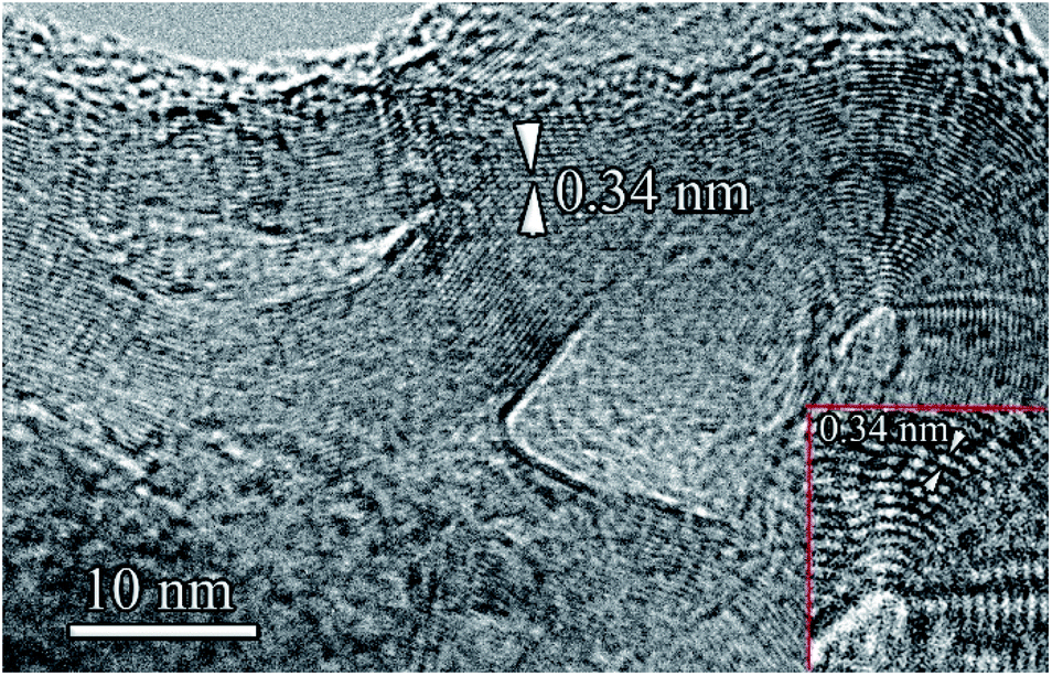
The microstructures of the second type, shown in Fig. 4b, are onion-like spheroids with diameters ranging from 10 to 100 nm. In contrast to classical onions, the resulting spheroids have a very high density of defects in the graphene planes. An enlarged bright-field TEM image is shown in Fig. 8a a. Rounded graphene planes with an interplanar spacing of 0.34 nm, determined from the electron diffraction pattern (Fig. 8b) and the corresponding histogram of the radially averaged intensity (Fig. 8c), are clearly visible. Evaluation of interplanar distances directly from HR TEM images showed that closer to the outer surface of the spheroids, the interplanar distance can increase to 0.37 nm. This may be because of the high defectiveness of the fibers. According to the studies by Borgardt et al.,48 an increase in the interplanar spacing in pyrolytic materials is associated with the depletion of the basal planes with carbon atoms.
 | ||
| Fig. 8 Results of studying the onion-like spheroids of the sample with a capacitance of 90 μF: (a) BF TEM image with an enlarged part of the edge of the spheroid, marked with a red rectangle in the inset. (b) Selected area electron diffraction pattern of the sample shown in a, arrows indicate rings indexed on (c). (c) Histogram of radially averaged intensity, indicated by peaks correspondent to the reflections of graphite. | ||
Typically, onion-like spheroids are stuck together to form hard-to-separate conglomerates. The form of the histogram of electron scattering intensity (Fig. 8c) with diffuse peaks 100/101, 004, and 110 and the absence of peaks 102, 103, and 104 correspond to the results of Kurdyumov and Pilyankevich,49 in which it is noted that this scattering pattern is characteristic of high-temperature pyrographite with a low degree of ordering.
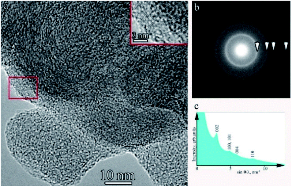
With a capacitor of 20090 μF, the destruction of benzene induced by low-voltage discharges, carbon microstructures are formed, for which the BF TEM image with a low magnification (overall BF TEM image) is shown in Fig. 9a. This sample also contained two types of microstructures. The first one is shown in Fig. 8a; onion-like spheroids, similar in morphology to the 90 μF found in the sample. The dimensions of the spheroids are on average smaller than in the sample of 90 μF and are in the range of 20–40 nm. The second type of microstructure is carbon fibers, which are indicated by arrows in Fig. 9a, and the HR TEM image is shown in Fig. 9b. The interplanar distances determined from HR TEM images were 0.35 ± 0.04 nm. The large scatter in the interplanar distances is most likely associated with the defectiveness of the graphene layers.
 | ||
| Fig. 9 (a) BF TEM image of the sample with a capacitor of 20090 μF. Arrows indicate areas containing graphite fibers. (b) An enlarged view of the fibers. (c) Selected area electron diffraction pattern of the sample. | ||
An electron diffraction pattern obtained from an area of the sample with a lateral dimension (diameter) of 200 nm is shown in Fig. 9c. It also indicates a high degree of disorder and small sizes of graphite fibers and onion-like spheroids. In the electron diffraction pattern, the arrows show diffuse rings, and the corresponding interplanar distances are close to 002, 100/101, and 110 2H hexagonal graphite. The rest of the reflections, as in the electron diffraction pattern shown in Fig. 8b, do not appear.
TEM of a sample of a carbon nanostructure obtained in the induced destruction of benzene with a capacitor of 40090 μF showed that the sample consisted exclusively of onion-like spheroids with a diameter of 20–40 nm, similar to those observed in the samples with a capacitor capacity of 20090 μF. The BF TEM image and corresponding electron diffraction patterns from the selected area are shown in Fig. 10.
 | ||
| Fig. 10 BF TEM image of the sample. The inset shows a selected area electron diffraction pattern of the sample. | ||
The electron diffraction pattern was almost identical to that obtained from the sample with a capacitor of 20090 μF. The arrows show the emerging diffuse rings and the corresponding interplanar distances, which are close to the 002, 100/101, and 110 2H hexagonal graphite. As in the sample obtained with a capacitor of 20090 μF, as well as in the electron diffraction pattern shown in Fig. 8b, the remaining reflexes are not manifested.
XRD patterns for three samples are shown in Fig. 11.
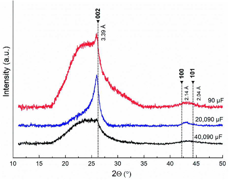 | ||
| Fig. 11 XRD patterns obtained from three benzole samples. | ||
The XRD patterns showed similar spectral characteristics and clear differences. In the three samples, a diffuse maximum from the X-ray amorphous component was found, starting from 17.5–18° with a plateau at 22–23°. At the end of the plateau near an angle of 26°, a relatively small peak corresponding to an interplanar spacing of 0.34 nm appears in the sample obtained with a capacitor of 90 μF. This peak is much more intense in the spectrum obtained from the sample with a capacitor of 20090 μF and is practically absent in the spectrum of the sample with a capacitor of 40090 μF. Close, but less pronounced peaks in the XRD patterns of the three samples appear in the range of 44–45°. The highest intensity of all peaks was observed in the XRD pattern of the sample with a capacitor of 20090 μF. These data are consistent with the results of the electron microscopy studies. The broad hump at 2θ = 17–26° was associated with a high concentration of nanosized X-ray amorphous structures. In particular, at 40090 μF, this can be caused by a large scatter of interplanar distances in onion-like spheroids. Disordered interlayers of carbon layers can form in the interlayer spaces of the carbon microstructures. At a capacitance of 20090 μF, the formation of a relatively high concentration of turbostratic graphite in sample causes the appearance of an intense peak near 26°, which corresponds to an interplanar distance of 0.34 nm, close to d(002) in 2H graphite. Defects in the graphene layers in the form of carbon vacancies lead to an increase in the interplanar spacing, which is noticeable in the XRD patterns. The 002 reflection near 26° was the weakest in the sample with a capacitance of 90 μF. The decrease in intensity can be associated with a lower concentration of turbostratic graphite relative to other carbon nanostructures.
From the obtained results of the induced transformation of benzene, it can be seen that low-temperature pulsed discharges in liquid media represent a new effective method for stimulating the synthesis of carbon nanostructures, including the processes of destruction and polycondensation (assembly of active particles) of benzene. The main products of benzene transformation are carbon nanostructures, the morphology of which is determined by the energy of low-voltage discharges. Gaseous products consist mainly of hydrogen and acetylene (Table 3). Thus, for the destruction of benzene induced by low-voltage discharges, a clear relationship between the discharge energy and the shape of the allotropic forms of carbon formed for the first time.
Consequently, in the direction of benzene transformation, the effect of low-voltage discharges on reagents in the liquid phase is fundamentally different from the effects of high temperature (pyrolysis at 900 °C)44 and thermal plasma33 on benzene. From the data given in Table 3, it can be seen that the yield of hydrogen during the destruction of benzene for all studied energies of pulsed discharges is very high (77.1–79.4 mol%).
The use of a capacitor with a low capacity of 90 μF for the synthesis of carbon structures (Table 2) leads to a low yield of the carbon phase (17.4 wt%) and high energy consumption (0.87 kW h per 1 g of carbon nanostructures), but a mixture of carbon structures is formed (Table 4) with a large specific surface of 277 m2 g−1.
| Capacity, μF | Shape of structures | Characteristics |
|---|---|---|
| 90 | Graphite fibers (flakes) | Length 150 nm |
| Thickness 10–20 nm | ||
| Interplanar distance 0.345 nm | ||
| Two- and three-layer graphene sheets | Interplanar distance 0.345 nm | |
| Two- and three-layer hollow spheres | ||
| CNHs | ||
| Onion-like spheroids | Diameter 10–100 nm | |
| Interplanar distance 0.34–0.37 nm | ||
| 20090 |
Onion-like spheroids | Diameter 20–40 nm |
| Turbostratic graphite carbon fibers | Interplanar distance 0.35 ± 0.04 nm | |
| 40090 |
Onion-like spheroids | Diameter 20–40 nm |
In,41 a benzyl radical was obtained (in situ) from iodobenzene by stimulating the process with an alkali metal. The resulting radicals induce the conversion of benzene to amorphous carbon. In accordance with these results, it can be assumed that under the action of low-voltage discharges, the process begins with the cleavage of the C–H bond in benzene with the formation of radicals and atomic hydrogen. Furthermore, the hydrogen radical splits off another hydrogen atom of the benzyl radical or the original benzene molecule. The result is molecular hydrogen and a new benzyl radical or second radical center in the benzene molecule. The resulting products of the induced transformation of benzene show that the formed benzyl radicals (in situ) are converted into reaction products in two ways: with the rupture of carbon–carbon bonds of the benzene ring and recombination of multicentre radicals. The first pathway is responsible for the formation of acetylene and other hydrocarbons in small quantities. As a result of the second method, several sequential processes are realized, leading to the formation of solid-phase products.
Within the framework of the generally accepted genetic relationship of allotropic forms of carbon, it is most likely that the initial polyradical cyclic fragments bind to each other due to the recombination of radicals into a system of the graphene type with sp2-hybrid carbons. Under the action of low-voltage pulsed discharges, three-layer graphene sheets were formed.
Further, graphene and three-layer graphene sheets are “rolled” into single-layer and three-layer nanotubes, as well as into two- and three-layer hollow spheres. It can be assumed that the formation of graphite fibers, CNHs, and onions also occurs through carbon structures such as graphene or graphene multilayer sheets.
4. Conclusions
The presented results show that the polycondensation of liquid benzene induced by low-voltage discharges leads to the formation of carbon nanostructures with various morphologies, as well as acetylene and hydrogen. Thus, the action of low-voltage pulsed discharges in liquid media is an effective method for stimulating the destructive transformation of hydrocarbons through the formation of nanostructures. The particles generated by the discharge were “quenched” by the liquid medium in the reactor. Further, in the stage of relaxation, the “assembly” of particles into carbon and hydrocarbon structures occurs in a controlled manner.This study is the first to show that a change in the energy of low-voltage pulsed discharges in liquid media causes a change in the morphology of the resulting carbon nanostructures. Thus, with a capacitor of 90 μF, the transformation of benzene induced by low-voltage discharges leads to the formation of two types of carbon nanostructures. These carbon structures have a specific surface area of 277 m2 g−1. The nanostructures of the first type are graphene fibers and two- and three-layer hollow spheres. Some BF TEM images also show microstructures in the form of CNHs, which are two- and three-layer ellipsoids and closed nanotubes.
Microstructures of the second type are spheroids, similar to onion-like spheroids with a diameter of 10 to 100 nm. In contrast to classical onions, the resulting spheroids have a high density of defects in the graphene planes. Onion-like spheroids were connected to each other. The observed electron scattering pattern of the obtained spheroids is characteristic of high-temperature pyrographite with a low degree of ordering.
An increase in the power of the electric discharge leads to an increase in the yield of carbon structures from 17.4 wt% to 30.3–34.8 wt%, but the surface area decreases to 102–133 m2 g−1.
The BF TEM image shows that the induced destruction of benzene at a capacitor of 20090 μF also led to the formation of two types of nanostructures: onion-like spheroids and carbon fibers. It follows from the BF TEM image that the transformation of benzene in the liquid phase induced by non-thermal plasma leads to the formation of onion-like spheroids with a diameter of 20–40 nm.
Conflicts of interest
There are no conflicts to declare.Acknowledgements
results of the research work were obtained with the support of a grant from the President of the Russian Federation for state support of young Russian scientists (MK-16.2020.8 agreement no. 075-15-2020-095).This work was supported by the Ministry of Science and Higher Education within the State assignment FSRC “Crystallography and Photonics” RAS in part of transmission electron microscopy and microanalysis and XRD measurements and data analysis. TEM and XRD was performed using the equipment of the Shared Research Center FSRC “Crystallography and photonics” RAS.Notes and references
- I. Levchenko, S. Xu, G. Teel, D. Mariotti, M. L. R. Walker and M. Keidar, Recent progress and perspectives of space electric propulsion systems based on smart nanomaterials, Nat. Commun., 2018, 9, 879, DOI:10.1038/s41467-017-022697.
- P. J. Bruggeman, M. J. Kushner, B. R. Locke, J. G. E. Gardeniers, W. G. Graham, D. B. Graves, R. C. H. M. Hofman-Caris, D. Maric, J. P. Reid, E. Ceriani, D. Fernandez Rivas, J. E. Foster, S. C. Garrick, Y. Gorbanev, S. Hamaguchi, F. Iza, H. Jablonowski, E. Klimova, J. Kolb, F. Krcma, P. Lukes, Z. Machala, I. Marinov, D. Mariotti, S. Mededovic Thagard, D. Minakata, E. C. Neyts, J. Pawlat, Z. Lj Petrovic, R. Pflieger, S. Reuter, D. C. Schram, S. Schröter, M. Shiraiwa, B. Tarabova, P. A. Tsai, J. R. R. Verlet, T. Von Woedtke, K. R. Wilson, K. Yasui and G. Zvereva, Plasma-liquid interactions: a review and roadmap, Plasma Sources Sci. Technol., 2016, 25(5), 053002, DOI:10.1088/0963-0252/25/5/053002.
- G. Saito and T. Akiyama, Nanomaterial synthesis using plasma generation in liquid, J. Nanomater., 2015, 2015, 123696, DOI:10.1155/2015/123696.
- S. Nomura, H. Toyota, M. Tawara, H. Yamashita and K. Matsumoto, Fuel gas production by microwave plasma in liquid, Appl. Phys. Lett., 2006, 88, 231502, DOI:10.1063/1.2210448.
- Y. A. Lebedev, Microwave discharges in liquid dielectrics, Plasma Phys. Rep., 2017, 43, 685–695, DOI:10.1134/S1063780X17060101.
- K. A. Averin, Y. A. Lebedev, A. N. Shchegolikhin and M. Y. Yablokov, Nanosize carbon products formed in microwave discharge in liquid alkanes, Plasma Process, Polym, 2017, 14(9), e201600227, DOI:10.1002/ppap.201600227.
- Y. Ando, X. Zhao, T. Sugai and M. Kumar, Growing carbon nanotube, Mater. Today, 2004, 7(10), 22–29, DOI:10.1016/S1369-7021(04)00446-8.
- A. H. Sari, A. Khazali and S. S. Parhizgar, Synthesis and characterization of long-CNTs by electrical arc discharge in deionized water and NaCl solution, Int. Nano Lett., 2018, 8(1), 19–23, DOI:10.1007/s40089-018-0227-5.
- A. A. Ashkarran, Metal and metal oxide nanostructures prepared by electrical arc discharge method in liquids, J. Cluster Sci., 2011, 22(2), 233–266, DOI:10.1007/s10876-011-0376-4.
- T. A. Kareem and A. A. Kaliani, I-V characteristics and the synthesis of ZnS nanoparticles by glow discharge at the metal–ionic liquid interface, J. Plasma Phys., 2012, 78(2), 189–197, DOI:10.1017/S0022377811000560.
- T. A. Kareem and A. A. Kaliani, Glow discharge plasma electrolysis for nanoparticles synthesis, Ionics, 2012, 18(3), 315–327, DOI:10.1007/s11581-011-0639-y.
- S. Nomura, A. E. E. Putra, S. Mukasa, H. Yamashita and H. Toyota, Plasma decomposition of clathrate hydrates by 2.45 GHz microwave irradiation at atmospheric pressure, Appl. Phys. Express, 2011, 4(6), 066201, DOI:10.1143/APEX.4.066201.
- D. Mariotti, J. Patel, V. Svrecek and P. Maguire, Plasma–liquid interactions at atmospheric pressure for nanomaterials synthesis and surface engineering, Plasma Processes Polym., 2012, 9(11–12), 1074–1085, DOI:10.1002/ppap.201200007.
- J. M. Li, Fabrication of a carbon nanotube drive shaft component, Nanotechnology, 2004, 15, 551–554, DOI:10.1088/0957-4484/15/5/025.
- J. M. Li, Realizing Single-Crystalline Vertically-Oriented and High-Density Electrospun Nanofibril Bundles by Controlled Postcalcination, CrystEngComm, 2017, 19(25), 3392–3397, 10.1039/C7CE00847C.
- J. M. Li, 4 nm ZnO nanocrystals fabrication through electron beam irradiation on the surface of a ZnO nanoneedle formed by thermal annealing, CrystEngComm, 2017, 19(1), 32–39, 10.1039/c6ce02187e.
- E. Shibata, R. Sergienko, H. Suwa and T. Nakamura, Synthesis of amorphous carbon particles by an electric arc in the ultrasonic cavitation field of liquid benzene, Carbon, 2004, 42(4), 885–888, DOI:10.1016/j.carbon.2004.01.047.
- R. Sergiienko, S. Kim, E. Shibata and T. Nakamura, Structure of Fe-Pt alloy included carbon nanocapsules synthesized by an electric plasma discharge in an ultrasonic cavitation field of liquid ethanol, J. Nanopart. Res., 2010, 12(2), 481–491, DOI:10.1007/s11051-009-9677-z.
- R. Sergiienko, E. Shibata, A. Zentaro, D. Shindo, T. Nakamura and G. Qin, Formation and characterization of graphite encapsulated cobalt nanoparticles synthesized by electric discharge in an ultrasonic cavitation field of liquid ethanol, Acta Mater., 2007, 55(11), 3671–3680, DOI:10.1016/j.actamat.2007.02.017.
- N. Sano, H. Wang, I. Alexandrou, M. Chhowalla, K. B. K. Teo, G. A. J. Amaratunga and K. Iimura, Properties of carbon onions produced by an arc discharge in water, J. Appl. Phys., 2002, 92, 2783–2788, DOI:10.1063/1.1498884.
- P. Muthakarn, N. Sano, T. Charinpanitkul, W. Tanthapanichakoon and T. Kanki, Characteristics of carbon nanoparticles synthesized by a submerged arc in alcohols, alkanes, and aromatics, J. Phys. Chem. B, 2006, 110(37), 18299–18306, DOI:10.1021/jp063443j.
- S. Bandow, F. Kokai, K. Takahashi, M. Yudasaka, L. C. Qin and S. Iijima, Interlayer spacing anomaly of single-wall carbon nanohorn aggregate, Chem. Phys. Lett., 2000, 321(5–6), 514–519, DOI:10.1016/S0009-2614(00)00353-5.
- E. Bekyarova, K. Murata, M. Yudasaka, D. Kasuya, S. Iijima, H. Tanaka, H. Kahoh and K. Kaneko, Single-wall nanostructured carbon for methane storage, J. Phys. Chem., 2003, 107(20), 4681–4684, DOI:10.1021/jp0278263.
- K. I. Baskakova, O. V. Sedelnikova, E. V. Lobiak, P. E. Plyusnin, L. G. Bulusheva and A. V. Okotrub, Modification of structure and conductivity of nanohorns by toluene addition in carbon arc, Fuller. Nanotube. Carbon Nanostructures, 2020, 28(4), 342–347, DOI:10.1080/1536383X.2019.1708737.
- N. Karousis, I. SuarezMartinez, C. P. Ewels and N. Tagmatarchis, Structure, properties, functionalization, and applications of carbon nanohorns, Chem. Rev., 2016, 116(8), 4850–4883, DOI:10.1021/acs.chemrev.5b00611.
- T. Sugai, H. Yoshida, T. Shimada, T. Okazaki, H. Shinohara and S. Bandow, New synthesis of high-quality double-walled carbon nanotubes by high-temperature pulsed arc discharge, Nano Lett., 2003, 3(6), 769–773, DOI:10.1021/nl034183+.
- R. B. Mathur, S. Seth, C. Lal, R. Rao, B. P. Singh, T. L. Dhami and A. M. Rao, Co-synthesis, purification and characterization of single- and multi-walled carbon nanotubes using the electric arc method, Carbon, 2007, 45(1), 132–140, DOI:10.1016/j.carbon.2006.07.027.
- T. Okada, T. Kaneko and R. Hatakeyama, Conversion of toluene into carbon nanotubes using arc discharge plasmas in solution, Thin Solid Films, 2007, 515(9), 4262–4265, DOI:10.1016/j.tsf.2006.02.067.
- B. Shen, J. Ding, X. Yan, W. Feng, J. Li and Q. Xue, Influence of different buffer gases on synthesis of few-layered graphene by arc discharge method, Appl. Surf. Sci., 2012, 258(10), 4523–4531, DOI:10.1016/j.apsusc.2012.01.019.
- Y. Wu, T. Zhang, F. Zhang, Y. Wang, Y. Ma, Y. Huang, Y. Liu and Y. Chen, In situ synthesis of graphene/single-walled carbon nanotube hybrid material by arc-discharge and its application in supercapacitors, Nano Energy, 2012, 1(6), 820–827, DOI:10.1016/j.nanoen.2012.07.001.
- L. E. Murr, D. K. Brown, E. V. Esquivel, T. D. Ponda, F. Martinez and A. Virgen, Carbon nanotubes and other fullerenes produced from tire powder injected into an electric arc, Mater. Charact., 2005, 55(4–5), 371–377, DOI:10.1016/j.matchar.2005.07.013.
- T. Sugai, H. Omote, S. Bandow, N. Tanaka and H. Shinohara, Production of fullerenes and single-wall carbon nanotubes by high-temperature pulsed arc discharge, J. Chem. Phys., 2000, 112(13), 6000, DOI:10.1063/1.481172.
- F. Cataldo, D. A. García-Hernández and A. Manchado, Toluene pyrolysis in an electric ARC: products analysis, Fuller. Nanotub. Carbon Nanostructures, 2019, 27(6), 469–477, DOI:10.1080/1536383X.2019.1576639.
- X. Ma, S. Li, R. Chaudhary, V. Hessel and F. Gallucci, Carbon Nanosheets Synthesis in a Gliding Arc Reactor: On the Reaction Routes and Process Parameters, Plasma Chem. Plasma Process., 2021, 41(2021), 191–209, DOI:10.1007/s11090-020-10120-z.
- P. Bruggeman and C. Leys, Non-thermal plasmas in and in contact with liquids, J. Phys. D: Appl. Phys., 2009, 42(5), 053001, DOI:10.1088/0022-3727/42/5/053001.
- I. V. Bodrikov, A. M. Kut'in, E. Y. Titov, D. Y. Titov, Y. A. Kurskii and R. R. Gazizzulin, Fragmentation of thiophene and 3-methyl-2-thiophenecarboxaldehyde by direct liquid phase low-voltage discharges, Plasma Process, Polym, 2018, 15, e1800094, DOI:10.1002/ppap.201800094.
- I. V. Bodrikov, E. Y. Titov, A. Y. Subbotin, I. I. Grinvald, D. Y. Titov and E. N. Razov, Condensation of chloromethanes and their binary systems with triphenylphosphine induced by low-voltage discharges, Plasma Process, Polym, 2020, 17(9), e1900247, DOI:10.1002/ppap.201900247.
- I. V. Bodrikov, E. Y. Titov, I. I. Grinvald, D. Y. Titov, Y. A. Kurskii and E. N. Razov, Doping effect of triphenylphosphine in the condensation of tetrachloromethane induced by low-voltage discharges, High Energy Chem., 2020, 54, 72–75, DOI:10.1134/S0018143920010026.
- I. Mochida, Y. Korai, C. H. Ku, F. Watanabe and Y. Sakai, Chemistry of synthesis, structure, preparation and application of aromatic-derived mesophase pitch, Carbon, 2000, 38(2), 305–328, DOI:10.1016/S0008-6223(99)00176-1.
- D. A. García-Hernández, A. Manchado, M. Gemmi, E. Mugnaioli, F. Fabbri, S. Pascale and F. Cataldo, Raman, FT-IR spectroscopy and morphology of carbon dust from carbon arc in liquid benzene, Fuller. Nanotub. Carbon Nanostructures, 2018, 26(10), 654–660, DOI:10.1080/1536383X.2018.1461623.
- G. P. Yong, X. R. Zhang, W. L. She and B. Zhang, Easy synthesis of hydrogenated amorphous carbon from benzene, Carbon, 2013, 55, 369–371, DOI:10.1016/j.carbon.2012.12.065.
- P. Serp, R. Feurer, Ph. Kalck, Y. Kihn, J. L. Faria and J. L. Figueiredo, A chemical vapor deposition process for the production of carbon nanospheres, Carbon, 2001, 39(4), 615–628, DOI:10.1016/S0008-6223(00)00324-9.
- H. S. Qian, F. M. Han, B. Zhang, Y. C. Guo, J. Yue and B. X. Peng, Noncatalytic CVD preparation of carbon spheres with a specific size, Carbon, 2004, 42(4), 761–766, DOI:10.1016/j.carbon.2004.01.004.
- L. Frusteri, C. Cannilla, K. Barbera, S. Perathoner, G. Centi and F. Frusteri, Carbon growth evidences as a result of benzene pyrolysis, Carbon, 2013, 59, 296–307, DOI:10.1016/j.carbon.2013.03.022.
- E. Y. Titov, D. Y. Titov, I. V. Bodrikov, A. M. Kutin, Y. A. Kurskii and R. R. Gazizzulin, A device for generation of low-voltage discharges in liquid dielectric media, High Energy Chem., 2019, 52, 512–513, DOI:10.1134/S0018143918060152.
- M. Bortolato, S. Dugaria, F. Agresti, S. Barison, L. Fedele, E. Sani and D. Del Col, Investigation of a single wall carbon nanohorn-based nanofluid in a full-scale direct absorption parabolic trough solar collector, Energy Convers. Manage., 2017, 150, 693–703, DOI:10.1016/j.enconman.2017.08.044.
- U. Hofmann and D. Wilm, Ueber die Kristallstruktur von Kohlenstoff, Z. Elektrochem., 1936, 42, 504–522 CAS.
- N. I. Borgardt, A. S. Prihodko and M. Seibt, The influence of the atomic structure of basal planes on interplanar distance in pyrolytic carbon materials, Tech. Phys. Lett., 2016, 42(12), 1137–1140, DOI:10.1134/S106378501612004X.
- A. V. Kurdyumov and A. N. Pilyankevich, Online intensities on X-ray patterns of graphite structures, Crystallography, 1968, 13(2), 311–315 CAS.
| This journal is © The Royal Society of Chemistry 2021 |