 Open Access Article
Creative Commons Attribution 3.0 Unported Licence
Modulation of the electronic structure and thermoelectric properties of orthorhombic and cubic SnSe by AgBiSe2 alloying†
Sushmita
Chandra
ad,
Raagya
Arora
bc,
Umesh V.
Waghmare
cd and
Kanishka
Biswas
 *ad
*ad
aNew Chemistry Unit, Jawaharlal Nehru Centre for Advanced Scientific Research (JNCASR), Jakkur P.O., Bangalore 560064, India. E-mail: kanishka@jncasr.ac.in
bChemistry and Physics of Materials Unit, Jawaharlal Nehru Centre for Advanced Scientific Research (JNCASR), Jakkur P.O., Bangalore 560064, India
cTheoretical Sciences Unit, Jawaharlal Nehru Centre for Advanced Scientific Research (JNCASR), Jakkur P.O., Bangalore 560064, India
dSchool of Advanced Materials and International Centre for Materials Science, Jawaharlal Nehru Centre for Advanced Scientific Research (JNCASR), Jakkur P.O., Bangalore 560064, India
First published on 31st August 2021
Abstract
Recently, single-crystals of tin selenide (SnSe) have drawn immense attention in the field of thermoelectrics due to their anisotropic layered crystal structure and ultra-low lattice thermal conductivity. Layered SnSe has an orthorhombic crystal structure (Pnma) at ambient conditions. However, the cubic rock-salt phase (Fm![[3 with combining macron]](https://www.rsc.org/images/entities/char_0033_0304.gif) m) of SnSe can only be stabilized at very high pressure and thus, the experimental realization of the cubic phase remains elusive. Herein, we have successfully stabilized the high-pressure cubic rock-salt phase of SnSe by alloying with AgBiSe2 (0.30 ≤ x ≤ 0.80) at ambient temperature and pressure. The orthorhombic polycrystalline phase is stable in (SnSe)1−x(AgBiSe2)x in the composition range of 0.00 ≤ x < 0.28, which corresponds to narrow band gap semiconductors, whereas the band gap closes upon increasing the concentration of AgBiSe2 (0.30 ≤ x < 0.70) leading to the cubic rock-salt structure. We confirmed the stabilization of the cubic structure at x = 0.30 and associated changes in the electronic structure using first-principles theoretical calculations. The pristine cubic SnSe exhibited the topological crystalline insulator (TCI) quantum phase, but the cubic (SnSe)1−x(AgBiSe2)x (x = 0.33) showed a semi-metallic electronic structure with overlapping conduction and valence bands. The cubic polycrystalline (SnSe)1−x(AgBiSe2)x (x = 0.30) sample showed n-type conduction at room temperature, while the orthorhombic (SnSe)1−x(AgBiSe2)x (0.00 ≤ x < 0.28) samples retained p-type character. Thus, by optimizing the electronic structure and the thermoelectric properties of polycrystalline SnSe, a high zT of 1.3 at 823 K has been achieved in (SnSe)0.78(AgBiSe2)0.22.
m) of SnSe can only be stabilized at very high pressure and thus, the experimental realization of the cubic phase remains elusive. Herein, we have successfully stabilized the high-pressure cubic rock-salt phase of SnSe by alloying with AgBiSe2 (0.30 ≤ x ≤ 0.80) at ambient temperature and pressure. The orthorhombic polycrystalline phase is stable in (SnSe)1−x(AgBiSe2)x in the composition range of 0.00 ≤ x < 0.28, which corresponds to narrow band gap semiconductors, whereas the band gap closes upon increasing the concentration of AgBiSe2 (0.30 ≤ x < 0.70) leading to the cubic rock-salt structure. We confirmed the stabilization of the cubic structure at x = 0.30 and associated changes in the electronic structure using first-principles theoretical calculations. The pristine cubic SnSe exhibited the topological crystalline insulator (TCI) quantum phase, but the cubic (SnSe)1−x(AgBiSe2)x (x = 0.33) showed a semi-metallic electronic structure with overlapping conduction and valence bands. The cubic polycrystalline (SnSe)1−x(AgBiSe2)x (x = 0.30) sample showed n-type conduction at room temperature, while the orthorhombic (SnSe)1−x(AgBiSe2)x (0.00 ≤ x < 0.28) samples retained p-type character. Thus, by optimizing the electronic structure and the thermoelectric properties of polycrystalline SnSe, a high zT of 1.3 at 823 K has been achieved in (SnSe)0.78(AgBiSe2)0.22.
Introduction
Thermoelectric materials can perform the conversion of waste heat into electricity and are believed to be the key to future energy management. In general, the performance of a thermoelectric material is determined by the dimensionless figure of merit, zT, which is given by zT = S2σ/κ, where σ, S, κ and T are the electrical conductivity, Seebeck coefficient, total thermal conductivity and absolute temperature, respectively.1–3 The total thermal conductivity is the sum of electrical thermal conductivity (κele) and lattice thermal conductivity (κlat). In a typical degenerate semiconductor, all the above-mentioned parameters, except κlat, are intertwined with each other in a trade-off fashion.1 Reduction in the κlat can be acquired by introducing crystal defects, alloying and nanostructuring,4–9 or by intrinsic phenomena.10,11 Amplification of the power factor (S2σ) is generally achieved by the improvement of the Seebeck coefficient through band convergence12,13 and resonance level formation.14 In addition, an enhancement of the electrical conductivity can be achieved through optimization of the carrier concentration by suitable doping.12–15 However, it remains a key challenge to optimally consolidate all these interdependent parameters in a single material to achieve high thermoelectric performance.The persistent search for efficient thermoelectric materials in the last few years has been intense, systematic, and multipronged, leading to the discovery of new two-dimensional (2D) layered materials with significantly high thermoelectric performances.16–18 However, the extraordinary discovery of layered tin selenide (SnSe) from the group IV–VI metal chalcogenide family has stimulated huge excitement in the thermoelectric community.19–30 Single-crystals of p-type SnSe showed an unprecedented zT of 2.6 at 923 K along the crystallographic b-axis,19 whereas, n-type SnSe single crystals exhibited a record-high zT of 2.8 at 773 K along the a-axis.21 The superior thermoelectric performance of SnSe single crystals arises from its intrinsically ultralow lattice thermal conductivity (0.20 W m−1 K−1) that primarily originates from the presence of high anharmonicity and anisotropy in its crystal structure.19,23
SnSe crystalizes in three different structures: the stable orthorhombic (Pnma) phase at ambient temperature and pressure,19,20 the metastable orthorhombic (Cmcm) phase at high temperature,23 and the unstable rock-salt cubic (Fm![[3 with combining macron]](https://www.rsc.org/images/entities/char_0033_0304.gif) m) phase at high pressure.31–33 SnSe undergoes a displacive phase transition from the low-symmetry Pnma phase to the high-symmetry Cmcm phase at ∼800 K.23 This phase transition at elevated temperature results in extended defects and enhancement in the lattice strain, which degrade the mechanical properties of SnSe and limit its long-term power generation applications at high temperature.34 Furthermore, it has been reported that the high-symmetry cubic phase can only be stabilized at very high pressure or by inducing strain.31–33,35 However, the formation energy calculated from the density functional theory (DFT) for the orthorhombic Pnma and cubic Fm
m) phase at high pressure.31–33 SnSe undergoes a displacive phase transition from the low-symmetry Pnma phase to the high-symmetry Cmcm phase at ∼800 K.23 This phase transition at elevated temperature results in extended defects and enhancement in the lattice strain, which degrade the mechanical properties of SnSe and limit its long-term power generation applications at high temperature.34 Furthermore, it has been reported that the high-symmetry cubic phase can only be stabilized at very high pressure or by inducing strain.31–33,35 However, the formation energy calculated from the density functional theory (DFT) for the orthorhombic Pnma and cubic Fm![[3 with combining macron]](https://www.rsc.org/images/entities/char_0033_0304.gif) m states are thermodynamically comparable.31,36 The cubic SnSe has been theoretically predicted to have large anharmonicity, high Seebeck coefficient and intrinsically low lattice thermal conductivity.32,36 Previously, cubic rock-salt SnSe was obtained in thin films grown on a Bi2Se3 substrate using molecular beam epitaxy;37 however, since it is a resource-consuming physical preparation process, an alternative method to prepare the cubic SnSe in bulk form is desired. Therefore, in this work, a chemical approach has been explored to stabilize the cubic rock-salt structure of SnSe and study the crystal and electronic structural evolution. Hitherto, the stabilization of cubic rock-salt polycrystalline SnSe has only been achieved via alloying with cubic rock salt AgSbSe2 and AgSbTe2.34,36,38 On the other hand, hexagonal AgBiSe2 has been successfully used to tune the carrier concentration and reduce the lattice thermal conductivity in the cubic phase of GeTe and GeSe systems.39,40 Hence, AgBiSe2 can be chosen as a suitable alloying material to tune the crystal structure, electrical and thermal properties of SnSe since it is isostructural to GeSe.
m states are thermodynamically comparable.31,36 The cubic SnSe has been theoretically predicted to have large anharmonicity, high Seebeck coefficient and intrinsically low lattice thermal conductivity.32,36 Previously, cubic rock-salt SnSe was obtained in thin films grown on a Bi2Se3 substrate using molecular beam epitaxy;37 however, since it is a resource-consuming physical preparation process, an alternative method to prepare the cubic SnSe in bulk form is desired. Therefore, in this work, a chemical approach has been explored to stabilize the cubic rock-salt structure of SnSe and study the crystal and electronic structural evolution. Hitherto, the stabilization of cubic rock-salt polycrystalline SnSe has only been achieved via alloying with cubic rock salt AgSbSe2 and AgSbTe2.34,36,38 On the other hand, hexagonal AgBiSe2 has been successfully used to tune the carrier concentration and reduce the lattice thermal conductivity in the cubic phase of GeTe and GeSe systems.39,40 Hence, AgBiSe2 can be chosen as a suitable alloying material to tune the crystal structure, electrical and thermal properties of SnSe since it is isostructural to GeSe.
Herein, we have successfully stabilized the high-pressure cubic rock-salt phase of SnSe by alloying with AgBiSe2 (0.30 ≤ x ≤ 0.80) at ambient temperature and pressure. The solid solution mixing of AgBiSe2 with SnSe increases the configurational entropy by introducing atomic disorder into the system and consequently stabilizes the cubic phase under ambient conditions. The orthorhombic polycrystalline phase is stable in (SnSe)1−x(AgBiSe2)x in the composition range of 0.00 ≤ x < 0.28, which corresponds to narrow band gap semiconductors. The band gap closes upon increasing the concentration of AgBiSe2 (0.30 ≤ x < 0.70) leading to the cubic rock-salt phase, which is consistent with the electronic structure calculated by DFT with the inclusion of spin orbit coupling. Interestingly, pristine cubic SnSe exhibits a topological crystalline insulator (TCI) quantum phase where the metallic surface states are protected by mirror symmetry, but the cubic (SnSe)1−x(AgBiSe2)x (x = 0.33) possesses a semi-metallic electronic structure with overlapping conduction and valence bands. Cubic polycrystalline (SnSe)1−x(AgBiSe2)x (x = 0.30) sample show n-type conduction at room temperature but the orthorhombic (SnSe)1−x(AgBiSe2)x (0.00 ≤ x < 0.28) samples retain their p-type character. Orthorhombic (SnSe)0.78(AgBiSe2)0.22 exhibits superior electrical conductivity and power factors of ∼685 S cm−1 and ∼6.50 μW cm−1 K−2, respectively, at 823 K. As a result, a peak zT of 1.3 at 823 K has been obtained in the polycrystalline orthorhombic (SnSe)0.78(AgBiSe2)0.22 system. This study provides profound insight into the crystal and electric structural modulations and thermoelectric properties of polycrystalline (SnSe)1−x(AgBiSe2)x.
Results and discussion
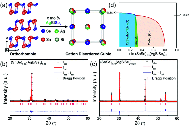
Polycrystalline (SnSe)1−x(AgBiSe2)x (0.00 ≤ x ≤ 1.00) samples were synthesized in a vacuum-sealed tube reaction followed by ball milling and spark plasma sintering (SPS). Orthorhombic SnSe (Pnma), when alloyed with AgBiSe2, gradually transformed from orthorhombic to the face-centered cubic structure under ambient conditions. With the addition of 30 mol% AgBiSe2 in SnSe, a disordered rock-salt (Fm![[3 with combining macron]](https://www.rsc.org/images/entities/char_0033_0304.gif) m) phase was stabilized (Fig. 1a), which realized up to 80 mol% AgBiSe2 addition in SnSe. The room-temperature powder X-ray diffraction (PXRD) patterns of bulk (SnSe)1−x(AgBiSe2)x samples can be indexed to the phase-pure orthorhombic phase when 0.00 ≤ x < 0.28, and to the face-centered cubic phase when 0.30 ≤ x ≤ 0.80 (Fig. S1, ESI†). On the contrary, the AgBiSe2-rich polycrystalline (SnSe)1−x(AgBiSe2)x (when x > 0.80) samples resemble the room temperature hexagonal crystal structure of AgBiSe2 (space group P
m) phase was stabilized (Fig. 1a), which realized up to 80 mol% AgBiSe2 addition in SnSe. The room-temperature powder X-ray diffraction (PXRD) patterns of bulk (SnSe)1−x(AgBiSe2)x samples can be indexed to the phase-pure orthorhombic phase when 0.00 ≤ x < 0.28, and to the face-centered cubic phase when 0.30 ≤ x ≤ 0.80 (Fig. S1, ESI†). On the contrary, the AgBiSe2-rich polycrystalline (SnSe)1−x(AgBiSe2)x (when x > 0.80) samples resemble the room temperature hexagonal crystal structure of AgBiSe2 (space group P![[3 with combining macron]](https://www.rsc.org/images/entities/char_0033_0304.gif) m1). The Rietveld refinement of the room temperature PXRD patterns of orthorhombic (SnSe)0.78(AgBiSe2)0.22 and cubic (SnSe)0.70(AgBiSe2)0.30 are shown in Fig. 1b and c, respectively, which indicate that when AgBiSe2 is added to the SnSe system, the Ag and Bi atoms preferentially occupy the Sn sites and induce disorder (Tables S1 and S2, ESI†). This leads to the enhancement of the configurational entropy and the consequent stabilization of the high symmetry cubic phase under ambient conditions. A similar phenomenon can also be observed in other alloys where, the addition of extra elements can boost the total entropy of the system, resulting in the stabilization of higher symmetric phases.39,41,42
m1). The Rietveld refinement of the room temperature PXRD patterns of orthorhombic (SnSe)0.78(AgBiSe2)0.22 and cubic (SnSe)0.70(AgBiSe2)0.30 are shown in Fig. 1b and c, respectively, which indicate that when AgBiSe2 is added to the SnSe system, the Ag and Bi atoms preferentially occupy the Sn sites and induce disorder (Tables S1 and S2, ESI†). This leads to the enhancement of the configurational entropy and the consequent stabilization of the high symmetry cubic phase under ambient conditions. A similar phenomenon can also be observed in other alloys where, the addition of extra elements can boost the total entropy of the system, resulting in the stabilization of higher symmetric phases.39,41,42
Field emission scanning electron microscopy (FESEM) in the backscattered electron mode (BSE) was performed on orthorhombic (SnSe)0.78(AgBiSe2)0.22 and cubic (SnSe)0.70(AgBiSe2)0.30 to check the purity of the polycrystals, which confirmed the absence of any secondary micro-precipitates (Fig. S2 and S3, ESI†) in both the samples. Energy dispersive X-ray (EDAX) elemental color mapping of Sn, Ag, Bi, and Se during FESEM for both the orthorhombic and cubic (SnSe)1−x(AgBiSe2)x (Fig. S4 and S5, ESI†) confirmed that all the elements were uniformly distributed in the samples, indicating the homogeneity of the polycrystals.
The schematic phase diagram of the SnSe–AgBiSe2 system, as inferred from PXRD, DSC, and TGA analysis, is shown in Fig. 1d; the phase boundaries are, however, relative to the position of the orthorhombic, and cubic phases with respect to the AgBiSe2 concentration. Nevertheless, this schematic phase diagram clearly shows that the increase in the AgBiSe2 concentration in SnSe causes a structural phase evolution from the orthorhombic to the rock-salt crystal structure.
The band gap of the pristine orthorhombic SnSe was measured to be about 0.90 eV (Fig. 2a), which is consistent with previous literature reports.19,20 However, when SnSe was alloyed with AgBiSe2, the band gap closed rapidly near to zero at x = 0.30 (Fig. 2a and b) owing to the increase in the chemical pressure originating from a decrease in the unit cell volume from 213 Å3 (orthorhombic) to 206 Å3 (cubic) as shown in Fig. 2c. The band-gap evolution plot is shown in Fig. 2b, which depicts that upon increasing the concentration of AgBiSe2 above x = 0.24, the band gap closes. The probable reason could be the structural phase transition induced contraction of the unit cell volume, which increased the chemical pressure and consequently reduced the band gap.
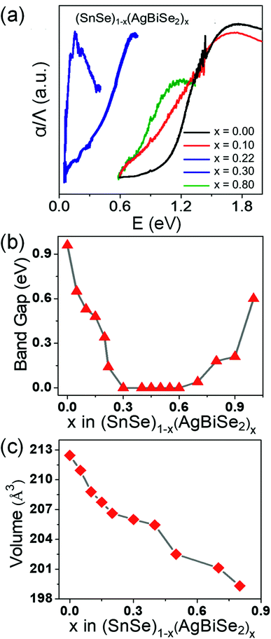 | ||
| Fig. 2 (a) Electronic absorption spectra, (b) band gap evolution and (c) unit cell volume of (SnSe)1−x(AgBiSe2)x (0.00 ≤ x ≤ 0.80) as a function of AgBiSe2 concentration. | ||
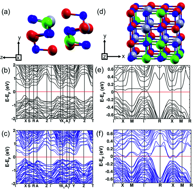
To study the evolution of the band gap with respect to alloying concentration, we used first-principles DFT calculations to determine the electronic band structure at three concentrations: pure SnSe (orthorhombic and cubic), (SnSe)0.80(AgBiSe2)0.20 (orthorhombic) and (SnSe)0.67(AgBiSe2)0.33 (cubic). The theoretical band gap of SnSe in the orthorhombic structure is 0.71 eV, with the inclusion of the spin–orbit coupling in calculations (Fig. S6, ESI†). Such underestimation of the band gap relative to the experimental band gap of 0.90 eV is typical of DFT calculations. We found that the theoretical band gap of SnSe decreased with AgBiSe2 alloying, consistent with the trend observed in experimental measurements using diffuse reflectance spectroscopy. The modelled structure of the orthorhombic (SnSe)0.80(AgBiSe2)0.20 generated using the special quasi-random structures (SQS) algorithm is shown in Fig. 3a. Our estimations of the band gap of (SnSe)0.80(AgBiSe2)0.20 are ∼0.51 eV and ∼0.24 eV without and with the inclusion of the spin–orbit coupling, respectively, as shown in Fig. 3b and c. The band gap obtained from calculation with spin orbit coupling is smaller than the experimentally observed value of ∼0.34 eV, as expected.
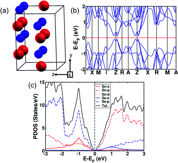
(SnSe)1−x(AgBiSe2)x with x = 0.33 exists in the cubic phase (Fm![[3 with combining macron]](https://www.rsc.org/images/entities/char_0033_0304.gif) m). The electronic structure of pure cubic SnSe exhibited a band gap of 0.12 eV estimated with the inclusion of the spin–orbit coupling in calculations as shown in Fig. 4. Examination of the projected density of states (PDOS) (Fig. 4c) revealed that its valence band (VB) was contributed mostly by p orbitals of Se, and weakly by s and p orbitals of Sn. The conduction band (CB) was contributed primarily by the p orbitals of Sn. We determined the mirror Chern number (nM)31,43 and the Z2 topological invariant of pure cubic SnSe. Z2 characterizes the topological insulators (TI) (Z2 = 0 trivial insulator and Z2 = 1 nontrivial insulator) and the mirror Chern number is the topological invariant describing a topological crystalline insulator (TCI). In topological crystalline insulators (TCI),43,44 the gapless surface states are protected by mirror symmetry, in contrast to topological insulators where the time-reversal symmetry protects the surface states. The presence of mirror symmetry in the crystal structure of a material results in the presence of planes in the BZ giving rise to mirror symmetry-protected Dirac cones in the surface electronic structure. A TCI supports an even number of Dirac cones and band inversions in sharp contrast to a TI characterized by odd numbers of band inversions. TCIs are characterized by a non-zero mirror Chern number. The individual Chern numbers C+i and C−i are defined on a mirror-invariant plane for TCI. The mirror Chern number43 defined as nM = (C+i − C−i)/2 can be used as a topological invariant for TCI. The strong Z2 topological invariant (ν0) of the cubic SnSe is 0 (normal insulator) confirming its trivial electronic topology with respect to time reversal symmetry, while its nM = 2 establishes its non-trivial band topology with respect to crystalline symmetry. Therefore, the cubic phase of SnSe is a TCI.
m). The electronic structure of pure cubic SnSe exhibited a band gap of 0.12 eV estimated with the inclusion of the spin–orbit coupling in calculations as shown in Fig. 4. Examination of the projected density of states (PDOS) (Fig. 4c) revealed that its valence band (VB) was contributed mostly by p orbitals of Se, and weakly by s and p orbitals of Sn. The conduction band (CB) was contributed primarily by the p orbitals of Sn. We determined the mirror Chern number (nM)31,43 and the Z2 topological invariant of pure cubic SnSe. Z2 characterizes the topological insulators (TI) (Z2 = 0 trivial insulator and Z2 = 1 nontrivial insulator) and the mirror Chern number is the topological invariant describing a topological crystalline insulator (TCI). In topological crystalline insulators (TCI),43,44 the gapless surface states are protected by mirror symmetry, in contrast to topological insulators where the time-reversal symmetry protects the surface states. The presence of mirror symmetry in the crystal structure of a material results in the presence of planes in the BZ giving rise to mirror symmetry-protected Dirac cones in the surface electronic structure. A TCI supports an even number of Dirac cones and band inversions in sharp contrast to a TI characterized by odd numbers of band inversions. TCIs are characterized by a non-zero mirror Chern number. The individual Chern numbers C+i and C−i are defined on a mirror-invariant plane for TCI. The mirror Chern number43 defined as nM = (C+i − C−i)/2 can be used as a topological invariant for TCI. The strong Z2 topological invariant (ν0) of the cubic SnSe is 0 (normal insulator) confirming its trivial electronic topology with respect to time reversal symmetry, while its nM = 2 establishes its non-trivial band topology with respect to crystalline symmetry. Therefore, the cubic phase of SnSe is a TCI.
We have examined the electronic structure of cubic (SnSe)1−x(AgBiSe2)x in two disordered configurations at x = 0.33 (Fig. S7a and S8a, ESI†) simulated with the model √2 × √2 × 1 supercell of the conventional cell of the Fm![[3 with combining macron]](https://www.rsc.org/images/entities/char_0033_0304.gif) m structure. The lower-symmetric disordered structure (Fig. S8a, ESI†) was simulated by interchanging a pair of Sn and Ag atoms in the first disordered structure (Fig. S7a, ESI†). The electronic structures in both cases showed a vanishing band gap with overlapping valence and conduction bands at the Fermi level, consistent with the trend observed in our experiments. In cubic SnSe (Fig. 4a), Sn occupies 4a (0.0, 0.0, 0.0) Wyckoff positions and Se occupies 4b (0.5, 0.5, 0.5) positions in the Fm
m structure. The lower-symmetric disordered structure (Fig. S8a, ESI†) was simulated by interchanging a pair of Sn and Ag atoms in the first disordered structure (Fig. S7a, ESI†). The electronic structures in both cases showed a vanishing band gap with overlapping valence and conduction bands at the Fermi level, consistent with the trend observed in our experiments. In cubic SnSe (Fig. 4a), Sn occupies 4a (0.0, 0.0, 0.0) Wyckoff positions and Se occupies 4b (0.5, 0.5, 0.5) positions in the Fm![[3 with combining macron]](https://www.rsc.org/images/entities/char_0033_0304.gif) m space group. In the cubic phase of SnSe alloyed with 33 mol% AgBiSe2, the Ag and Bi atoms occupy any of the 4a (0, 0, 0) sites randomly; therefore, to take into account the effect of realistic chemical disorder we generated a model structure using the SQS algorithm. In the 2 × 2 × 2 supercell having 16 Sn, 8 Ag, 8 Bi and 32 Se atoms, 4b Wyckoff sites are occupied by Se atoms while Ag, Bi and Sn atoms randomly occupy 4a sites (Fig. 3d). Our estimation of the band gap of cubic (SnSe)0.67(AgBiSe2)0.33 calculated without spin–orbit coupling (Fig. 3e) is ∼0.07 eV, whereas the inclusion of the spin–orbit coupling closes this small gap and confirms its semi-metallic nature (Fig. 3f). For a deeper understanding of the electronic properties, we examined the projected density of states (PDOS) of the cubic phase of (SnSe)0.67(AgBiSe2)0.33 (Fig. S7c, ESI†). The valence band is dominated by the contribution from the p-orbitals of Se, similar to pure cubic SnSe, while the CB is contributed majorly by the p orbitals of Sn and along with additional new contributions from p-orbitals of Bi.
m space group. In the cubic phase of SnSe alloyed with 33 mol% AgBiSe2, the Ag and Bi atoms occupy any of the 4a (0, 0, 0) sites randomly; therefore, to take into account the effect of realistic chemical disorder we generated a model structure using the SQS algorithm. In the 2 × 2 × 2 supercell having 16 Sn, 8 Ag, 8 Bi and 32 Se atoms, 4b Wyckoff sites are occupied by Se atoms while Ag, Bi and Sn atoms randomly occupy 4a sites (Fig. 3d). Our estimation of the band gap of cubic (SnSe)0.67(AgBiSe2)0.33 calculated without spin–orbit coupling (Fig. 3e) is ∼0.07 eV, whereas the inclusion of the spin–orbit coupling closes this small gap and confirms its semi-metallic nature (Fig. 3f). For a deeper understanding of the electronic properties, we examined the projected density of states (PDOS) of the cubic phase of (SnSe)0.67(AgBiSe2)0.33 (Fig. S7c, ESI†). The valence band is dominated by the contribution from the p-orbitals of Se, similar to pure cubic SnSe, while the CB is contributed majorly by the p orbitals of Sn and along with additional new contributions from p-orbitals of Bi.
We calculated the relative stabilities of the orthorhombic and cubic phases of (SnSe)1−x(AgBiSe2)x with varied x (where x = 0, 0.20, 0.33) to confirm the transformation of the orthorhombic SnSe (Pnma) into the face-centered cubic structure with AgBiSe2 alloying. Here, we used the same SQS supercell in the calculation of cubic and orthorhombic structures at each value of x by deforming and distorting the cubic structure to the orthorhombic structure and relaxing it further. For pristine SnSe, the orthorhombic phase is lower in energy with respect to its cubic phase by 2 meV f.u.−1 confirming its greater stability as seen in the experimental results. At 20% AgBiSe2 alloying, the orthorhombic phase remains lower in energy by ∼46 meV f.u.−1 with respect to its cubic phase, consistent with the experimentally observed orthorhombic structure of (SnSe)0.80(AgBiSe2)0.20. Our estimation of the energy difference between the orthorhombic and cubic (SnSe)0.67(AgBiSe2)0.33 was 1620 meV f.u.−1, stabilizing the cubic phase over its orthorhombic phase, confirming that the rock-salt (Fm![[3 with combining macron]](https://www.rsc.org/images/entities/char_0033_0304.gif) m) phase is stabilized with the addition of 30 mol% AgBiSe2 in SnSe.
m) phase is stabilized with the addition of 30 mol% AgBiSe2 in SnSe.
Thermoelectric properties were measured for the ball-milled and SPS-processed anisotropic orthorhombic and isotropic cubic polycrystalline (SnSe)1−x(AgBiSe2)x (0.00 ≤ x ≤ 0.30) samples. The cubic polycrystalline (SnSe)0.70(AgBiSe2)0.30 sample showed lower thermoelectric performance as compared to the orthorhombic (SnSe)0.78(AgBiSe2)0.22. On the other hand, improved thermoelectric performance was observed in the anisotropic orthorhombic phase when measurements were carried out parallel to the SPS pressing direction (Fig. S9, ESI†).
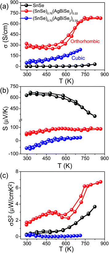
Fig. 5 presents the thermoelectric properties of (SnSe)1−x(AgBiSe2)x (0.00 ≤ x ≤ 0.30) measured parallel to the SPS pressing direction. Fig. 5a depicts the temperature-dependent electrical conductivity of the pristine orthorhombic SnSe, orthorhombic (SnSe)0.78(AgBiSe2)0.22 and cubic (SnSe)0.70(AgBiSe2)0.30. The σ of the pristine orthorhombic SnSe was 1.18 S cm−1 at 300 K, which increased to about 270 S cm−1 upon 22 mol% AgBiSe2 alloying at room temperature. For all the (SnSe)1−x(AgBiSe2)x (0.00 ≤ x < 0.28) samples, electrical conductivity increased with increasing temperature, which indicated the semiconducting transport (Fig. 5a). The sharp increase in electrical conductivity at 610 K for orthorhombic (SnSe)0.78(AgBiSe2)0.22 is an indication of the phase transition from lower symmetric Pnma to the higher symmetric Cmcm phase.24,45 The solid-solution mixing of AgBiSe2 with SnSe significantly increased σ due to the enhancement in the carrier concentration from 8.9 × 1017 cm−3 for pristine SnSe to 8.2 × 1019 cm−3 in (SnSe)0.78(AgBiSe2)0.22. A positive value of the Hall coefficient indicated that holes are the majority carriers in orthorhombic (SnSe)1−x(AgBiSe2)x (0.00 ≤ x < 0.28) making it a p-type semiconductor (Table S3, ESI†). Further, on addition of 30 mol% AgBiSe2, the sample became n-type in nature as confirmed from the negative sign of the Hall coefficient and the room temperature carrier concentration was 6.17 × 1018 cm−3 for the cubic (SnSe)0.70(AgBiSe2)0.30.
The measured value of the Seebeck coefficient of the pristine orthorhombic SnSe was 631 μV K−1 at 300 K (Fig. 5b), which decreased to 46 μV K−1 for orthorhombic (SnSe)0.78(AgBiSe2)0.22 and with a further increase in the AgBiSe2 concentration, the sample showed n-type conduction with an S value of −57 μV K−1 for (SnSe)0.70(AgBiSe2)0.30. The lower value of the Seebeck coefficient was consistent with the high carrier concentration in these samples. However, the cubic (SnSe)0.70(AgBiSe2)0.30 showed an anomalous trend in the S values arising mainly due to the onset of bipolar conduction. Due to the optimization in carrier concentration and electrical conductivity, a moderate power factor of ∼6.52 μW cm−1 K−2 was achieved in the (SnSe)0.78(AgBiSe2)0.22 sample at 873 K (Fig. 5c).
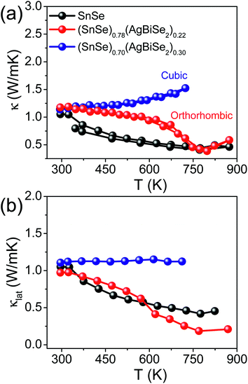
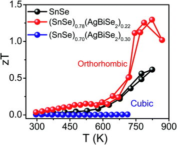
The total thermal conductivity of the pristine orthorhombic SnSe, orthorhombic (SnSe)0.78(AgBiSe2)0.22 and cubic (SnSe)0.70(AgBiSe2)0.30 measured parallel to the SPS pressing direction are presented in Fig. 6a. However, the room temperature total thermal conductivity is higher for the (SnSe)1−x(AgBiSe2)x (x = 0.22 and 0.30) samples as compared to the pristine SnSe, which arises mainly due to the greater contributions from the electrical thermal conductivity (Fig. S10, ESI†). Ball-milled and SPS-processed pristine SnSe exhibited a lattice thermal conductivity (κlat) of 1.08 W m−1 K−1 at 300 K, which decreased to 0.43 W m−1 K−1 at 773 K (Fig. 6b). When SnSe was alloyed with AgBiSe2, κlat in the cubic (SnSe)0.70(AgBiSe2)0.30 increased significantly to ∼1.13 W m−1 K−1 at 300 K (Fig. 6b). The low lattice thermal conductivity in orthorhombic SnSe was mainly caused by the damping phonon vibrations due to the presence of significant lattice anharmonicity.19,20 However, in the as-prepared cubic (SnSe)0.70(AgBiSe2)0.30, the higher lattice thermal conductivity can be attributed to the destruction of the layered orthorhombic crystal structure of SnSe. The orthorhombic (SnSe)0.78(AgBiSe2)0.22 sample showed an ultralow lattice thermal conductivity of ∼0.19 W m−1 K−1 at 773 K due to the enhanced phonon scattering induced by the point defects due to the entropy-driven solid solution in the SnSe–AgBiSe2 system in addition to lattice anharmonicity. The ultra-low κlat of (SnSe)0.78(AgBiSe2)0.22 at high temperature is comparable to that of the other high-performance SnSe-based polycrystalline samples (Table S5, ESI†). Thus, as a collective result of improved carrier concentration, elevated power factor and low thermal conductivity, a high zT of 1.3 has been achieved in the polycrystalline orthorhombic (SnSe)0.78(AgBiSe2)0.22 sample at 823 K (Fig. 7) when measured parallel to the SPS pressing direction, which is reversible and reproducible for different batches of samples, as well as for heating–cooling cycles (Fig. S11, ESI†).
Conclusions
The electronic and crystal structures of SnSe have been tailored with the addition of AgBiSe2. The layered orthorhombic phase is stable in (SnSe)1−x(AgBiSe2)x in the composition range of 0.00 ≤ x < 0.28, which corresponds to narrow band gap semiconductors. The high-pressure cubic rock-salt phase of SnSe has been stabilized under ambient conditions with increasing AgBiSe2 concentration to 0.30 ≤ x ≤ 0.80. Solid solution mixing of AgBiSe2 with SnSe increased the configurational entropy by introducing atomic disorder into the system and consequently stabilized the cubic phase under ambient conditions. The anomalous closing of the band gap of SnSe with increasing AgBiSe2 concentration was caused by the influence of the increase in chemical pressure. Electronic structures of the orthorhombic and cubic phases of (SnSe)1−x(AgBiSe2)x showed the emergence of the band gap at higher AgBiSe2 concentrations in SnSe. The pristine cubic SnSe exhibited a topological crystalline insulator (TCI) phase but the cubic (SnSe)1−x(AgBiSe2) (x = 0.33) showed a semi-metallic electronic structure with overlapping conduction and valence bands. While the cubic (SnSe)0.70(AgBiSe2)0.30 sample showed n-type conduction, the orthorhombic (SnSe)0.78(AgBiSe2)0.22 retained the p-type nature at room temperature. We have achieved a high zT of 1.3 in the p-type polycrystalline orthorhombic (SnSe)0.78(AgBiSe2)0.22 at 823 K via the optimization of the carrier concentration and electronic properties.Data availability
All data are available in the manuscript or in the ESI.†Author contributions
K. B. conceived the idea and designed the study. S. C. and K. B. carried out the synthesis, characterizations, thermoelectric experiments and analysis of data. R. A. and U. V. W. carried out the theoretical calculations. All authors contributed to writing the manuscript.Conflicts of interest
The authors declare no competing financial interest.Acknowledgements
We acknowledge funding support from SERB (CRG/2019/001306). KB acknowledges the funding support from Swarna-Jayanti Fellowship, DST (DST/SJF/CSA-02/2018-19) and Sheikh Saqr Fellowship. SC and RA acknowledge JNCASR, India for the fellowship.References
- G. Tan, L. D. Zhao and M. G. Kanatzidis, Chem. Rev., 2016, 116, 12123–12149 CrossRef CAS PubMed.
- X.-L. Shi, J. Zou and Z. G. Chen, Chem. Rev., 2020, 120, 7399–7515 CrossRef CAS PubMed.
- Y. Xiao and L. D. Zhao, Science, 2020, 367, 1196–1197 CrossRef CAS PubMed.
- S. Roychowdhury, T. Ghosh, R. Arora, M. Samanta, L. Xie, N. K. Singh, A. Soni, J. He, U. V. Waghmare and K. Biswas, Science, 2021, 371, 722–727 CrossRef CAS.
- K. Biswas, J. He, I. D. Blum, C.-I. Wu, T. P. Hogan, D. N. Seidman, V. P. Dravid and M. G. Kanatzidis, Nature, 2012, 489, 414–418 CrossRef CAS PubMed.
- K. Biswas, J. He, Q. Zhang, G. Wang, C. Uher, V. P. Dravid and M. G. Kanatzidis, Nat. Chem., 2011, 3, 160–166 CrossRef CAS PubMed.
- B. Poudel, Q. Hao, Y. Ma, Y. Lan, A. Minnich, B. Yu, X. Yan, D. Wang, A. Muto, D. Vashaee, X. Chen, J. Liu, M. S. Dresselhaus, G. Chen and Z. Ren, Science, 2008, 320, 634–638 CrossRef CAS PubMed.
- H. J. Wu, L. D. Zhao, F. S. Zheng, D. Wu, Y. L. Pei, X. Tong, M. G. Kanatzidis and J. Q. He, Nat. Commun., 2014, 5, 4515 CrossRef CAS PubMed.
- B. Jiang, Y. Yu, J. Cui, X. Liu, L. Xie, J. Liao, Q. Zhang, Y. Huang, S. Ning, B. Jia, B. Zhu, S. Bai, L. Chen, S. J. Pennycook and J. He, Science, 2021, 371, 830–834 CrossRef CAS PubMed.
- M. K. Jana and K. Biswas, ACS Energy Lett., 2018, 3, 1315–1324 CrossRef CAS.
- M. Dutta, D. Sarkar and K. Biswas, Chem. Commun., 2021, 57, 4751–4767 RSC.
- Y. Pei, X. Shi, A. LaLonde, H. Wang, L. Chen and G. J. Snyder, Nature, 2011, 473, 66–69 CrossRef CAS PubMed.
- M. Dutta, T. Ghosh and K. Biswas, APL Mater., 2020, 8, 040910 CrossRef CAS.
- J. P. Heremans, V. Jovovic, E. S. Toberer, A. Saramat, K. Kurosaki, A. Charoenphakdee, S. Yamanaka and G. J. Snyder, Science, 2008, 321, 554–557 CrossRef CAS PubMed.
- L. D. Zhao, V. P. Dravid and M. G. Kanatzidis, Energy Environ. Sci., 2014, 7, 251–268 RSC.
- Y. Zhou and L. D. Zhao, Adv. Mater., 2017, 29, 1702676 CrossRef.
- J. Wu, Y. Chen, J. Wu and K. Hippalgaonkar, Adv. Electron. Mater., 2018, 4, 1800248 CrossRef.
- M. Samanta, T. Ghosh, S. Chandra and K. Biswas, J. Mater. Chem. A, 2020, 8, 12226–12261 RSC.
- L. D. Zhao, S.-H. Lo, Y. Zhang, H. Sun, G. Tan, C. Uher, C. Wolverton, V. P. Dravid and M. G. Kanatzidis, Nature, 2014, 508, 373–377 CrossRef CAS.
- L. D. Zhao, G. Tan, S. Hao, J. He, Y. Pei, H. Chi, H. Wang, S. Gong, H. Xu, V. P. Dravid, C. Uher, G. J. Snyder, C. Wolverton and M. G. Kanatzidis, Science, 2016, 351, 141–144 CrossRef CAS.
- C. Chang, M. Wu, D. He, Y. Pei, C.-F. Wu, X. Wu, H. Yu, F. Zhu, K. Wang, Y. Chen, L. Huang, J.-F. Li, J. He and L. D. Zhao, Science, 2018, 360, 778–783 CrossRef CAS.
- A. T. Duong, V. Q. Nguyen, G. Duvjir, V. T. Duong, S. Kwon, J. Y. Song, J. K. Lee, J. E. Lee, S. Park, T. Min, J. Lee, J. Kim and S. Cho, Nat. Commun., 2016, 7, 13713 CrossRef CAS PubMed.
- L. D. Zhao, C. Chang, G. Tan and M. G. Kanatzidis, Energy Environ. Sci., 2016, 9, 3044–3060 RSC.
- S. Chandra and K. Biswas, J. Am. Chem. Soc., 2019, 141, 6141–6145 CrossRef CAS PubMed.
- W. Wei, C. Chang, T. Yang, J. Liu, H. Tang, J. Zhang, Y. Li, F. Xu, Z. Zhang, J. F. Li and G. Tang, J. Am. Chem. Soc., 2018, 140, 499–505 CrossRef CAS PubMed.
- J. Liu, P. Wang, M. Wang, R. Xu, J. Zhang, J. Liu, D. Li, N. Liang, Y. Du, G. Chen and G. Tang, Nano Energy, 2018, 53, 683–689 CrossRef CAS.
- G. Tang, W. Wei, J. Zhang, Y. Li, X. Wang, G. Xu, C. Chang, Z. Wang, Y. Du and L. D. Zhao, J. Am. Chem. Soc., 2016, 138, 13647–13654 CrossRef CAS PubMed.
- Y. K. Lee, Z. Luo, S. P. Cho, M. G. Kanatzidis and I. Chung, Joule, 2019, 3, 719–731 CrossRef CAS.
- X. Lou, S. Li, X. Chen, Q. Zhang, H. Deng, J. Zhang, D. Li, X. Zhang, Y. Zhang, H. Zeng and G. Tang, ACS Nano, 2021, 15, 8204–8215 CrossRef CAS.
- G. Tang, Q. Wen, T. Yang, Y. Cao, W. Wei, Z. Wang, Z. Zhang and Y. Li, RSC Adv., 2017, 7, 8258–8263 RSC.
- Y. Sun, Z. Zhong, T. Shirakawa, C. Franchini, D. Li, Y. Li, S. Yunoki and X.-Q. Chen, Phys. Rev. B: Condens. Matter Mater. Phys., 2013, 88, 235122 CrossRef.
- D. Wang, W. He, C. Chang, G. Wang, J. Wang and L. D. Zhao, J. Mater. Chem. C, 2018, 6, 12016–12022 RSC.
- S. ur Rehman, F. K. Butt, Z. Tariq, F. Hayat, R. Gilani and F. Aleem, J. Alloys Compd., 2017, 695, 194–201 CrossRef CAS.
- Y. Luo, S. Hao, S. Cai, T. J. Slade, Z. Z. Luo, V. P. Dravid, C. Wolverton, Q. Yan and M. G. Kanatzidis, J. Am. Chem. Soc., 2020, 142, 15187–15198 CrossRef CAS.
- Z. Wang, J. Wang, Y. Zang, Q. Zhang, J.-A. Shi, T. Jiang, Y. Gong, C.-L. Song, S.-H. Ji, L.-L. Wang, L. Gu, K. He, W. Duan, X. Ma, X. Chen and Q.-K. Xue, Adv. Mater., 2015, 27, 4150–4154 CrossRef CAS.
- H. Wang, H. Hu, N. Man, C. Xiong, Y. Xiao, X. Tan, G. Liu and J. Jiang, Mater. Today Phys., 2021, 16, 100298 CrossRef CAS.
- W. Jin, S. Vishwanath, J. Liu, L. Kong, R. Lou, Z. Dai, J. T. Sadowski, X. Liu, H. H. Lien, A. Chaney, Y. Han, M. Cao, J. Ma, T. Qian, J. I. Dadap, S. Wang, M. Dobrowolska, J. Furdyna, D. A. Muller, K. Pohl, H. Ding, H. G. Xing and R. M. Osgood, Phys. Rev. X, 2017, 7, 041020 Search PubMed.
- H. X. Wang, L. S. Mao, X. J. Tan, G. Q. Liu, J. T. Xu, H. Z. Shao, H. Y. Hu and J. Jiang, Nano Energy, 2018, 51, 649–655 CrossRef CAS.
- S. Roychowdhury, T. Ghosh, R. Arora, U. V. Waghmare and K. Biswas, Angew. Chem., Int. Ed., 2018, 57, 15167–15171 CrossRef CAS PubMed.
- M. Samanta, T. Ghosh, R. Arora, U. V. Waghmare and K. Biswas, J. Am. Chem. Soc., 2019, 141, 19505–19512 CrossRef CAS PubMed.
- D. Sarkar, T. Ghosh, S. Roychowdhury, R. Arora, S. Sajan, G. Sheet, U. V. Waghmare and K. Biswas, J. Am. Chem. Soc., 2020, 142, 12237–12244 CrossRef CAS.
- D. Sarkar, S. Roychowdhury, R. Arora, T. Ghosh, A. Vasdev, B. Joseph, G. Sheet, U. V. Waghmare and K. Biswas, Angew. Chem., Int. Ed., 2021, 60, 10350–10358 CrossRef CAS.
- J. C. Y. Teo, L. Fu and C. L. Kane, Phys. Rev. B: Condens. Matter Mater. Phys., 2008, 78, 045426 CrossRef.
- L. Fu, Phys. Rev. Lett., 2011, 106, 106802 CrossRef PubMed.
- S. Chandra, P. Dutta and K. Biswas, ACS Appl. Energy Mater., 2020, 3, 9051–9057 CrossRef CAS.
Footnote |
| † Electronic supplementary information (ESI) available. See DOI: 10.1039/d1sc03696c |
| This journal is © The Royal Society of Chemistry 2021 |

