Impact of changes in bond structure on ovonic threshold switching behaviour in GeSe2†
Received
27th August 2020
, Accepted 17th November 2020
First published on 19th November 2020
Abstract
Raman spectroscopy measurements are performed on sputtered GexSe1−x thin films to identify bond presence. A large amount of homopolar bonds are found, including Ge–Ge bonds that can be attributed to Ge clustering. A time-resolved approach to Raman spectroscopy is explored to observe the effect of the high power-density laser on the sample material. Several methods are then used to tailor the structural bond homogeneity (homopolar–heteropolar bonds): annealing, varying sputter deposition pressure and the addition of dopants. In particular doping can reduce homopolar bond presence and increase heteropolar bonds presence. The impact of each dopant is supported by calculations of bond enthalpies according to Pauling equation using the approach of Lankhorst/Bicerano–Ovshinsky. Finally, in order to correlate the structural bond presence to the Ovonic Threshold Switching behaviour of (doped) GexSe1−x thin films, both DC and pulsed (AC) measurement are performed on metal–insulator–metal (MIM) type test structures. It is found that minimizing homopolar bond presence is beneficial for the leakage current and electrical stability of the material.
1 Introduction
It is estimated that by 2025 the size of the Global Datasphere will exceed 175 zetabytes.1 This represents a more than five-fold increase in data storage over a timespan of 7 years. To accommodate the ever increasing demand for more storage, new types of memory technologies are being explored to provide alternatives to traditional storage devices that are faster, have a good scalability and a lower power consumption. Storage Class Memory (SCM) in particular is a class of memory that is gaining interest, providing a balance between long term storage capacity, density and fast read and write speeds. A promising candidate is non-volatile memory based on phase-changing materials2 which has all the above requirements and the additional benefit that it may be easily incorporated in 3D structured cross-bar architectures. These architectures effectively allow the stacking of multiple layers of memory cells on top of each other which greatly increases the memory density.3 However, they require every cell to be fitted with an additional acces device to eliminate unwanted sneak currents.4 Such an acces device is called a selector and needs to be compatible with the accompanying memory cell. As such, the tunability of the material used to make these devices is highly important. Chalcogenides are promising materials for two-terminal selectors based on Ovonic Threshold Switching (OTS).5 In this work, we investigate the impact of composition, deposition conditions and the addition of dopants on the chemical bond formation in Ge–Se based materials. An in-depth Raman analysis is carried out to understand the bond presence of the different films which is then combined with electrical measurements to correlate the occurrence of specific bonds with OTS performance. Understanding the impact of certain bonds on the electrical performance allows for more targeted engineering of selector materials.
2 Experimental
Using RF sputtering 50 nm thin films were deposited onto silicon and SiO2 substrates for Raman analysis and X-ray diffraction (XRD). GexSe1−x thin films with x ranging from 35% to 60% were deposited by co-sputtering from either a GeSe2 or a Ge2Se3 target in combination with a Ge target. As reference a 25 nm Ge layer was deposited as well. Standard deposition was performed in Ar at 5 × 10⁻³ mbar and the pressure was varied for a specific set of GeSe2 depositions between 3.8–50 × 10−3 mbar. Doping with Sb (14 to 26 at%) was achieved by sputtering from an Sb target and doping with N (3 to 10.6 at%) by reactive sputtering in a partial N2 atmosphere. Compositions were determined using a combination of Elastic Recoil Detection (ERD) and Rutherford Backscattering Spectrometry (RBS) measurements. Raman analysis was performed using a Horiba Jobin–Yvon LabRAM HR and a 9 mW 532 nm laser focused to a 1 μm spot size with ND transmission filters varying between 10% to 100%. Moreover, time-resolved results were obtained by taking spectra over short intervals in rapid succession over a total time scale of up to 2 minutes. For several samples, measurements were performed on two different locations on the sample to check for sample inhomogeneity. Differences in spectra between locations were negligible, indicating good sample homogeneity on the scale of the Raman measurement.
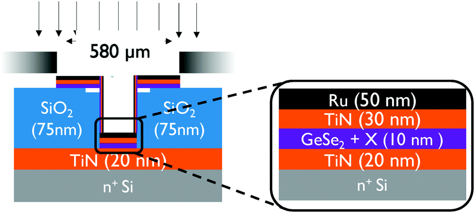
For electrical characterization experiments, separate samples were prepared with 10 nm thin films deposited in MIM type test structures where the bottom electrode is scaled to 5 μm. A schematic of the test structures can be found in Fig. 1. A patterned substrate is used consisting of a 75 nm SiO2 insulating layer on top of a 20 nm TiN bottom electrode layer. Then 5 μm diameter vias are patterned and etched in the SiO2 down to the bottom TiN. The switching and top electrode layers are sputtered through a 580 μm shadow mask aligned with the bottom electrode vias in the substrate. This results in large top electrode for easy contacting but an effective switching area diameter of only 5 μm.
 |
| | Fig. 1 Schematic of the test structures used for electrical characterisation. Layers are sputtered through a shadow mask onto a patterned substrate consisting of a 75 nm SiO2 layer with 5 μm vias on top of a 20 nm TiN bottom electrode layer. The final layer stack can be seen in the inset. | |
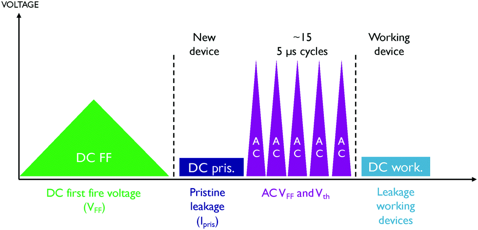
During the measurements, a positive voltage is applied to the top electrode while the backside of the sample is grounded. Using a Keithley 2601 SMU, a slow voltage ramp is performed to obtain the switching voltage when applying a normal DC voltage. This procedure will often result in a leaky cell and therefore is not used for detailed threshold voltage analysis but to select a lower voltage at which to determine the leakage current (Ipris) of the cell, prior to switching. Leakage current measurements are also done using DC conditions. To characterize the threshold switching behaviour, first the leakage current of a set of on average 10 pristine devices is measured at 2 V. Using a Keysight 81150A pulse generator in combination with a MSOX3104T mixed oscilloscope, short triangular voltage pulses with a rise and fall time of 2.5 μs are then used to obtain values for the first fire and threshold voltage (AC VFF and AC Vth). The short duration of the pulses ensures that the switching remains volatile. One channel of the oscilloscope measures the voltage drop across the sample while the second channel is used to measure the voltage drop over the 50 Ω input impedance to determine the current flowing through the cell. Switching parameters obtained using this method are prefixed by the letters AC to distinguish them from the DC switching voltages. Finally, on a set of working cells (cell that are not leaky after at least 15 cycles), a final DC measurement is done to measure the leakage current after operation. This measurement approach is graphically represented in Fig. 2.
 |
| | Fig. 2 Graphical representation of the sequence of electrical measurements used to characterize devices. | |
3 Results and discussion
3.1 Identifying bonds in GeSe2 with Raman spectroscopy
In order to study the relation between bond presence and electrical behaviour as well as the impact of certain (post)-deposition processes on both the structural and functional properties, first a thorough Raman study of the base material was performed. To accurately identify the bond structure, several compositions of GexSe1−x were measured with Raman spectroscopy ranging from a 35% Ge content up to 60% Ge content. Varying composition makes peak identification easier as certain peaks become more or less pronounced at different compositions. The Raman spectra of all compositions can be found in the supplementary material. For the purpose of this paper, only the 35% Ge was focussed on. This composition was sputtered from a single GeSe2 target to limit as much as possible fluctuations in the base material. For the remainder of this paper we will refer to this composition as a GeSe2 layer. Peak identification was done by comparing the measured spectra to results found in literature, both on chalcogenide thin films as well as bulk glasses. The expected peak positions for several relevant vibrational modes can be found in Table 1. A notable feature in PVD deposited thin film spectra is the presence of more homopolar bonds at the same composition as compared to bulk glasses. Additionally, peak widths tend to be broader in thin film spectra6,7 which indicates a larger degree of disorder (variations in bond length and angle).
Table 1 Raman vibrational modes in GeSex
| Label |
Bond |
Structure |
Expected Raman shift (cm−1) |
| I |
Ge–Ge |
Ge2Se3(ETH) |
170,8 175,9–11 180![[thin space (1/6-em)]](https://www.rsc.org/images/entities/char_2009.gif) 12,13 12,13 |
| II |
Ge–Se |
GeSe4 (CS) |
197–198,9–11 2008,13,14 |
| III |
Ge–Se |
GeSe4 (ES) |
213,9–11 214–2158,14 |
| IV |
Se–Se |
Se chains |
235,8 240–270,15 250–3009 |
| V |
Ge–Ge |
Amorph. Ge |
270,16 28017 |
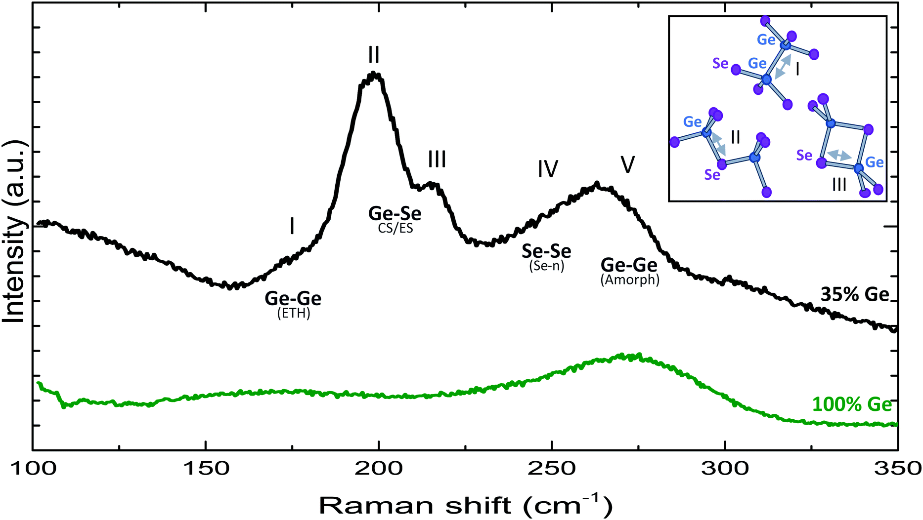
In Fig. 3 the Raman spectrum of the 35% Ge layer can be found as well as an amorphous 100% Ge reference layer. The shoulder peak I, around 175 cm−1, can be attributed to Ge–Ge modes in ethane-like Ge2(Se1/2)6 structural units as illustrated in the molecular representation. Peaks II and III, centred around 197 cm−1 and 217 cm−1 are related to GeSe4 tetrahedra that are connected by sharing Se atoms. Peak II corresponds to the symmetric stretching of Ge–Se–Ge linkages that are corner-shared (CS) whilst peak III corresponds to the breathing mode of a pair of Se atoms that are edge-shared (ES). Peak IV, centred around 250 cm−1 corresponds to the modes of a third structural unit that is rarely present in Ge rich layers but becomes more prominent as the Ge concentration approaches or drops below 33%. This broad peak, that overlaps partially with peak V, corresponds to stretching of Se–Se chains. Finally, peak V indicates a broad band stretching from 225–325 cm−1 that can be easily observed in the spectra of the Ge richer compositions (see ESI†) but is less distinguishable for the as-deposited 35% Ge layer as it overlaps partially with that of Se–Se modes. Specifically, this peak is also present in a pure Ge layer and is not dependent on the substrate material. The fact this peak is present in all examined GexSe1−x layers may suggest the presence of Ge clusters across all compositions supporting earlier hypotheses on the band gap and leakage current of GeSex.18 In the work by Valeri et al. it was observed that a direct band gap as determined by photoconductivity measurements remained constant for a GexSe1−x layer with varying Ge content while the leakage current showed a dramatic difference. This can be understood by the presence of Ge clusters whose distribution becomes denser as Ge content increases, resulting in higher leakage while not having a large impact on the material band gap.
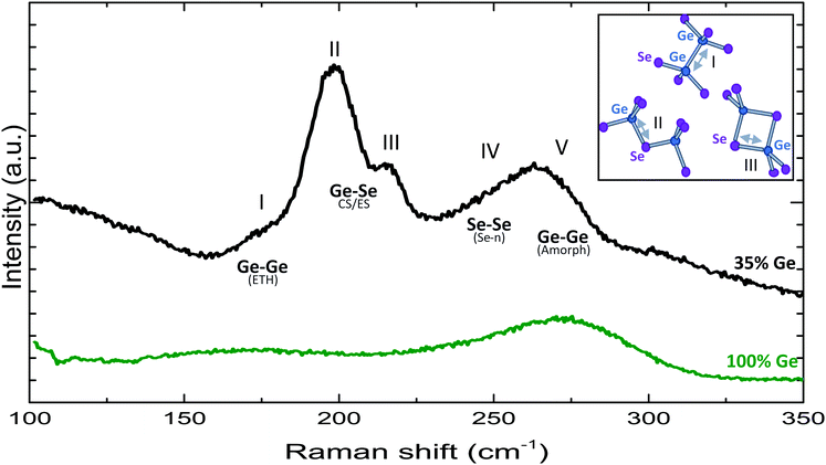 |
| | Fig. 3 Raman spectra of a 35% Ge layer with resolved peaks I–V. The inset shows a molecular representation of the configuration modes corresponding to peaks I–III. The spectrum of a pure Ge reference layer is also shown. | |
For a 35% Ge composition, peaks II and III are the most intense. This is expected as this composition is close to the 1–2 ratio of Ge to Se that make up the structural units that are responsible for these peaks. Furthermore there are other peaks noticeable. In particular, the shoulder peak I indicates that some structural units contain an excess of Ge bonds, likewise the high intensity in region IV denotes the presence of pure Se chains. From this it can be deduced that the glass is not in perfect chemical equilibrium. These “wrong bonds” may be a consequence of the PVD deposition process as the sputtered material that is deposited on the cold substrate does not have the time or temperature needed to reach equilibrium.
3.1.1 Time-resolved Raman approach.
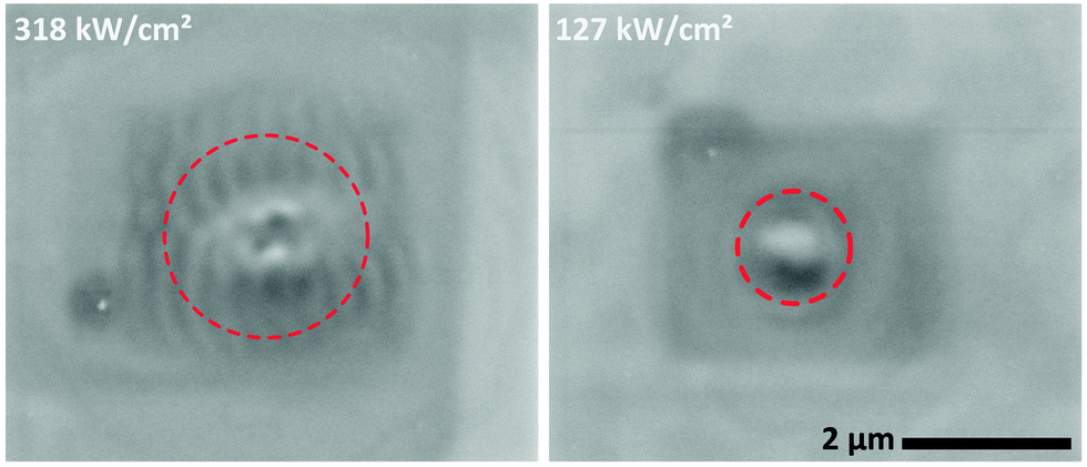
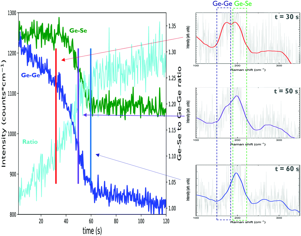
During the above experiments, a secondary effect was discovered when performing micro Raman analysis on thin film chalcogenides. Depending on the exposure times and laser power density, the laser can have a localised effect on the material itself. This can be seen from the scanning electron microscopy images in Fig. 4. Two images were taken of probed locations on the sample where a Raman measurement had occurred, at different power densities. During all the measurements shown so far, a spot size of 1 μm and a laser power of 1 mW was used (this equates to a theoretical power density of 127 kW cm−2). The exposure times of the spots in the image are also larger than those of a regular measurement. In order to determine the impact of the observed local modification on the Raman analysis, an alternative way of measuring was explored. Instead of a single data collection during a 100 s of exposure, short snapshots were collected in rapid succession under continuous laser illumination. To compensate for the decrease in signal-to-noise ratio, the laser power density was increased to 250% to gain more signal. It is also more instructive to look at the integrated intensity in certain regions of interest. This was tested for a 42% Ge layer and the results can been seen in Fig. 5. Two regions were compared: the region surrounding the 175 cm−1 peak related to the Ge–Ge bond vibrations of Ge2Se3 structural units and the region containing the 195 cm−1 and 217 cm−1 peaks related to Ge–Se bond vibrations of neighbouring GeSe4 tetrahedra. It can be seen from the analysis that the Ge–Ge bond modes rapidly decrease in intensity at the start of the measurement while the Ge–Se bond modes are stable for a longer time and start to decrease in intensity after roughly 40 seconds of continuous exposure. As such, the ratio of Ge–Se to Ge–Ge bonds increases overtime. Although at a different timescale, Clima et al.19 observed qualitatively the same picture from first principles simulations: the amount of Ge–Ge bonds decrease in time. This observation is in-line with their lower exothermicity if compared to Ge–Se bonds. The observed transition of high to low intensity is similar to that observed for an annealed layer that will be discussed in the next section which may suggest that the observed behaviour is thermal in nature. It is expected that the high laser power density, combined with the low thermal conductivity20,21 of the probed material results in localized heating of the layer.
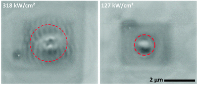 |
| | Fig. 4 High contrast SEM images of the measurement location probed by the laser during Raman measurement of a 42% Ge layer at two configurations of laser power and lens. The theoretical power density of the laser at the measurement spot is shown in the image, as well as the probed area. | |
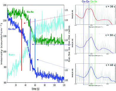 |
| | Fig. 5 Time-resolved Raman analysis of Ge42Se58. The left plot shows the integrated intensity of two regions in the Raman spectra as well as their ratio. The right images show 200 ms snapshot spectra at three total exposure times. The coloured lines are smoothed versions of the noisy spectra. It should be noted that the total laser power density during this measurement was 250% of that of a regular measurement. | |
A comparable study into the photostability of 600 nm Ge-rich (>33 at% Ge) chalcogenide layers9 reports a similar shift in bond presence, though on timescale of minutes to hours and using lower laser power density. Because of these conditions it can be expected that the achieved temperatures are lower. The transition in intensity is associated to an inherent difference in bond enthalpy of the Ge–Ge bonds compared to the Ge–Se bonds, causing instability of the bond structure under the laser illumination. Contributions other than thermal heating may also need consideration. A different study22 investigates photobleaching of Ge–Se layers and finds, for Ge2Se3 layers, that photobleaching under prolonged 660 nm laser irradiation only occurs in ambient air, but not in vacuum, suggesting a photo-oxidation which primarily attacks the Ge–Ge bonds. The photo-oxidation hypothesis is in agreement with a more recent study which is still ongoing that seems to indicate that a capping layer may prevent changes in the spectra during Raman analysis. Structural changes can be avoided by using a proper laser power density and a sufficiently short total measurement time. Care should also be taken the material is not exposed to the laser before the measurement is started. Taking this into account it is possible to obtain reliable Raman spectra of thin film chalcogenides. To determine the optimal settings, a time-resolved measurement can be done alongside regular measurements. As such, modest laser power densities and exposure times can be used to probe as-deposited film structure while higher laser powers and longer exposures may give insight into film stability. For the purpose of this paper, the same lower power and exposure time settings were chosen for all samples, based on the results for the base material, with verification time-resolved measurements performed on every sample. At these settings, no significant time-resolved effect could be observed for any sample.
3.2 Electrical characterization of GeSe2
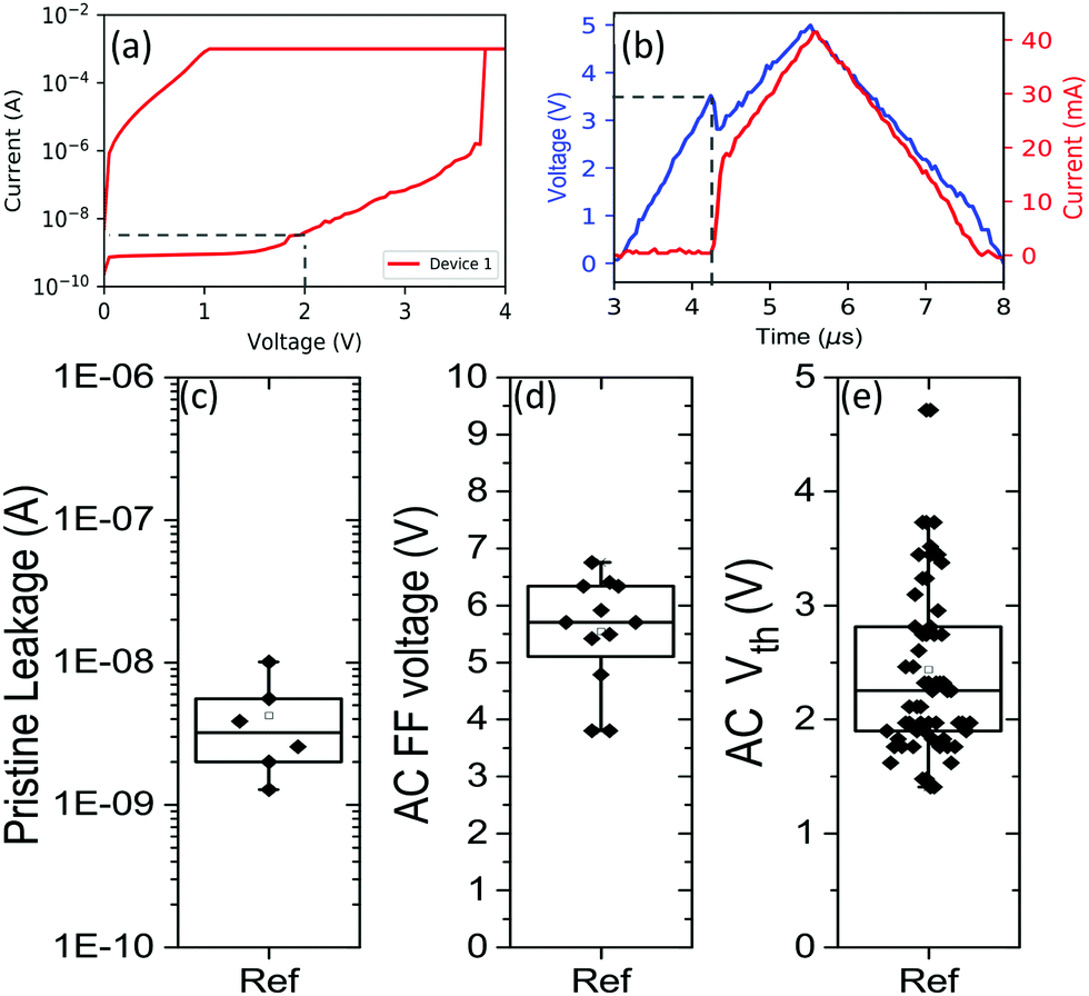
The electrical parameters for a 10 nm GeSe2 layer are summarized using a box plot representation in Fig. 6. Examples of typical measurements are also shown. Fig. 6a shows a typical DC IV sweep of a single cell. The point at which the pristine leakage current is determined is taken at 2 V, well below the DC first fire voltage of 3.8 V. Fig. 6b shows an example of a pulsed measurement. The blue curve represents the applied voltage while the red curve represent the current through the device. A python script was used to automatically determine the time at which the current displays a sharp increase and this timestamp is then used to determine the threshold voltage. As a base material GeSe2 has a relatively low off-state leakage current which is vitally important for OTS selectors. The first fire voltage VFF indicates the voltage at which the pristine material switches during the first cycle from a high-resistive state to a low resistive state. It acts as a measure of how difficult the material is to switch. The threshold voltage Vth is recorded from all the subsequent cycles and it is systematically lower than the first fire voltage, indicating the material goes through a certain conditioning step during the first fire.
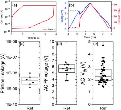 |
| | Fig. 6 IV data for 35% Ge as-deposited GeSe2. (a) DC voltage sweep, the dashed lines indicate the point at which pristine leakage is determined. (b) Pulsed AC voltage sweep, the dashed lines indicate the determined threshold voltage. (c) Pristine leakage of 7 cells. (d) pulsed first-fire voltage of 14 cells. (e) Threshold voltage of ±15 cycles of 4 working cells. | |
3.3 Annealing below TC
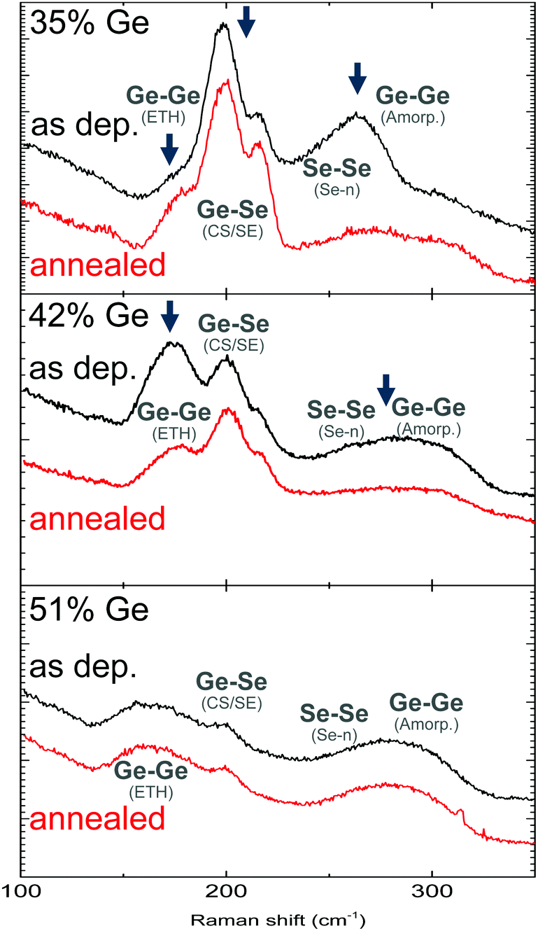
A first method that was investigated to tune bond structure concerns a post-deposition anneal of the material. Caution must be taken here that the crystallisation temperature is not exceeded as OTS is only observed in amorphous chalcogenides. Three different composition layers were annealed up to 250 °C and the amorphicity verified using XRD. The Raman spectra of the as deposited and annealed layers are shown in Fig. 7.
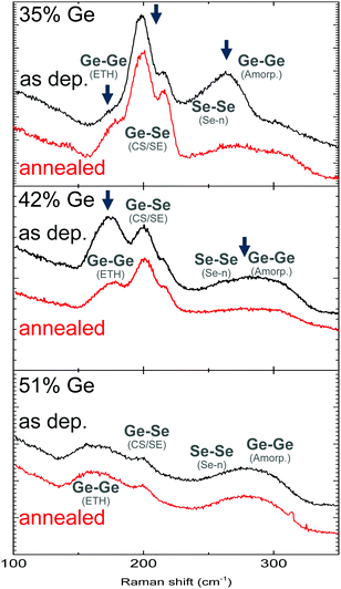 |
| | Fig. 7 Raman data of as deposited and annealed GexSe1−x layers. The arrows indicate peaks that are changing post anneal. | |
The exact impact of the anneal on the material is dependent on the composition. For a 35% Ge layer the intensity of the peaks relating to Se–Se chains and amorphous Ge clusters decreases, while an increase is observed in the intensity of the peaks relating to Ge–Se structural units. The largest increase is observed at 217 cm−1, which is related to edge-shared GeSe4 tetrahedra. A slight increase is also observed in the intensity of Ge–Ge modes relating to ethane-like Ge2Se3 complexes. These results mirror those reported by Pan et al.10 on PLD deposited GeSe2 films. The conversion of Se–Se and pure Ge–Ge homopolar bonds to form Ge–Se bonds can be understood by looking at their respective bond enthalpies (see Table 2). The appearance of slightly more Ge–Ge modes relating to ethane-like Ge2Se3 structural units may be an indirect result of a higher amount of Ge–Se bonds in general or where inside the material most of the conversion is taking place, for instance Ge–Se bonds forming in the direct vicinity of Ge clusters may result in more Ge rich structural units. For a 42% Ge there is a notable decrease in the intensity of Ge–Ge modes, both of Ge2Se3 complexes and pure Ge. Finally, for a 51% Ge layer, no change is observed in the Raman spectrum after anneal.
Table 2 Bond enthalpies in kJ mol−1 according to the Pauling equation27,28,30
| Ge–Se |
Ge–Ge |
Se–Se |
Ge–N |
Se–N |
Ge–Sb |
Se–Sb |
Sb–Sb |
Sb–N |
| 235 |
186 |
227 |
354 |
296 |
181 |
225 |
175 |
341 |
To study the impact on the electrical characteristics, a reference sample consisting of a 35% Ge switching layer was annealed and measured. The results are summarized in Fig. 8. Compared to the reference, the annealed devices were found to have a lower pristine leakage and a proportionally higher first fire voltage. This can be explained by the decreased amount of pure Ge clustering that is observed in this material. This is similar to the effect observed by doping with N that will be discussed later, which also targets homopolar Ge bonds. However, after first fire all cells were found to be leaky. This may be in part attributed to the higher first fire voltage since it results in a greater energy dissipation in the first fire event which in turn can cause local crystallisation or other effects which can lead to leaky cell, high first fire voltage also indicates that switching the material is more difficult in general. This could indicate that some amount of homopolar bonds and the associated defects are necessary to facilitate switching.
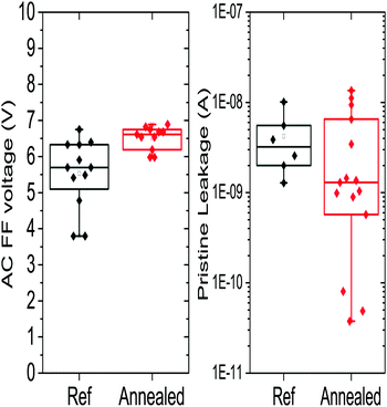 |
| | Fig. 8 IV data of the 35% Ge sample as-deposited and after anneal at 200 °C. No Vth data is shown as all devices of the annealed sample were found to be leaky after first fire. Data collected from at least 11 cells. | |
3.4 Varying deposition pressure
It may also be possible to tune bonds structure during the RF sputter deposition process. The effect of sputter gas pressure on the composition of chalcogenide films has been explored for GeSeSb films by Verget et al.23 They report that at a pressure of 5 × 10⁻³ mbar an increased amount of Ge–Ge bonds are present, compared to higher deposition pressure.
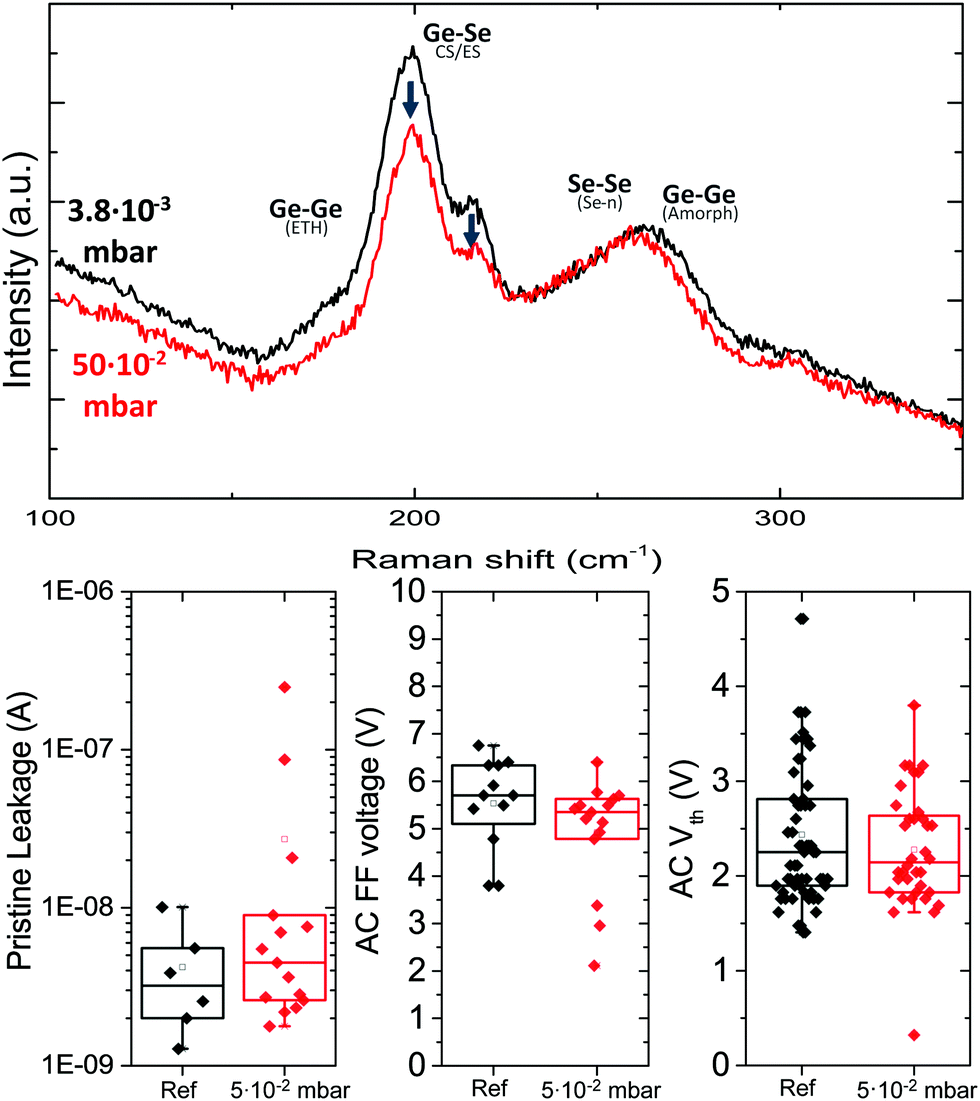
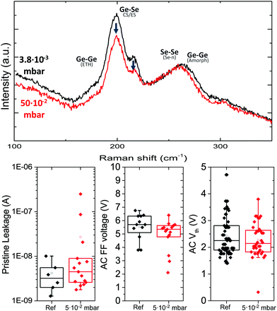
To allow for comparison with the doping in the next section, thin films were sputtered from a single GeSe2 target at pressures ranging from 3.8 × 10⁻³ mbar to 5 × 10⁻² mbar. The Raman and electrical results of the highest and lowest pressure are summarized in Fig. 9. It can be seen from the Raman analysis that despite an order of magnitude difference in the deposition pressure, no significant differences are observed in the Raman spectra of the two layers. When increasing the pressure to 5 × 10⁻² mbar the height of the peaks relating to Ge–Se modes is slightly lower in comparison to the height of the peak relating to Se chains and amorphous Ge modes, indicating the latter may be more present. An additional finding concerned a slight variation in composition with changing deposition pressures. Though all films are sputtered from a GeSe2 target, the film composition was found to be slightly richer in Ge, corresponding to about 35% Ge at the default pressure of 5 × 10⁻³ mbar. It was found that the maximum pressure, the Ge composition was 34.3% Ge while at the lowest pressure the composition was found to be 36.3% Ge. This indicates that at higher deposition pressures the film composition more closely reflects that of the target material while at lower pressures a Ge excess is observed. A similar observation was also reported by Verger et al.23 One might expect that this composition variation can be attributed to a difference in the transport of sputtered species. Indeed, different transport modes from ballistic to diffuse gas phase transport are observed during magnetron sputtering.24 However, in this case it would be expected that the lighter Ge would be more affected and scattered more compared to heavier Se, resulting in Se-richer films at intermediate pressures. This however, is not observed so an alternative explanation may be found in resputtering effects or sticking coefficients of sputtered species. A detailed study thereof is outside the scope of this paper. In regards to the IV measurement only minor differences are observed when the pressure is increased. The leakage current for the 5 × 10⁻² mbar film is slightly higher, with a corresponding lower AC FF voltage. There is no clear impact on the threshold voltage. It can be concluded thus that despite a factor 10 difference in the deposition pressure, and despite composition change, no significant differences are observed in the Raman spectra of the two layers nor electrical characteristics.
 |
| | Fig. 9 Raman and IV data of GeSe2 sputtered films at the lowest and highest deposition pressure. For the IV data, that of the reference layer, used in the previous paragraph is shown as the pressure used for this deposition is sufficiently close to that of the lowest deposition pressure. | |
3.5 Doping with Sb and N
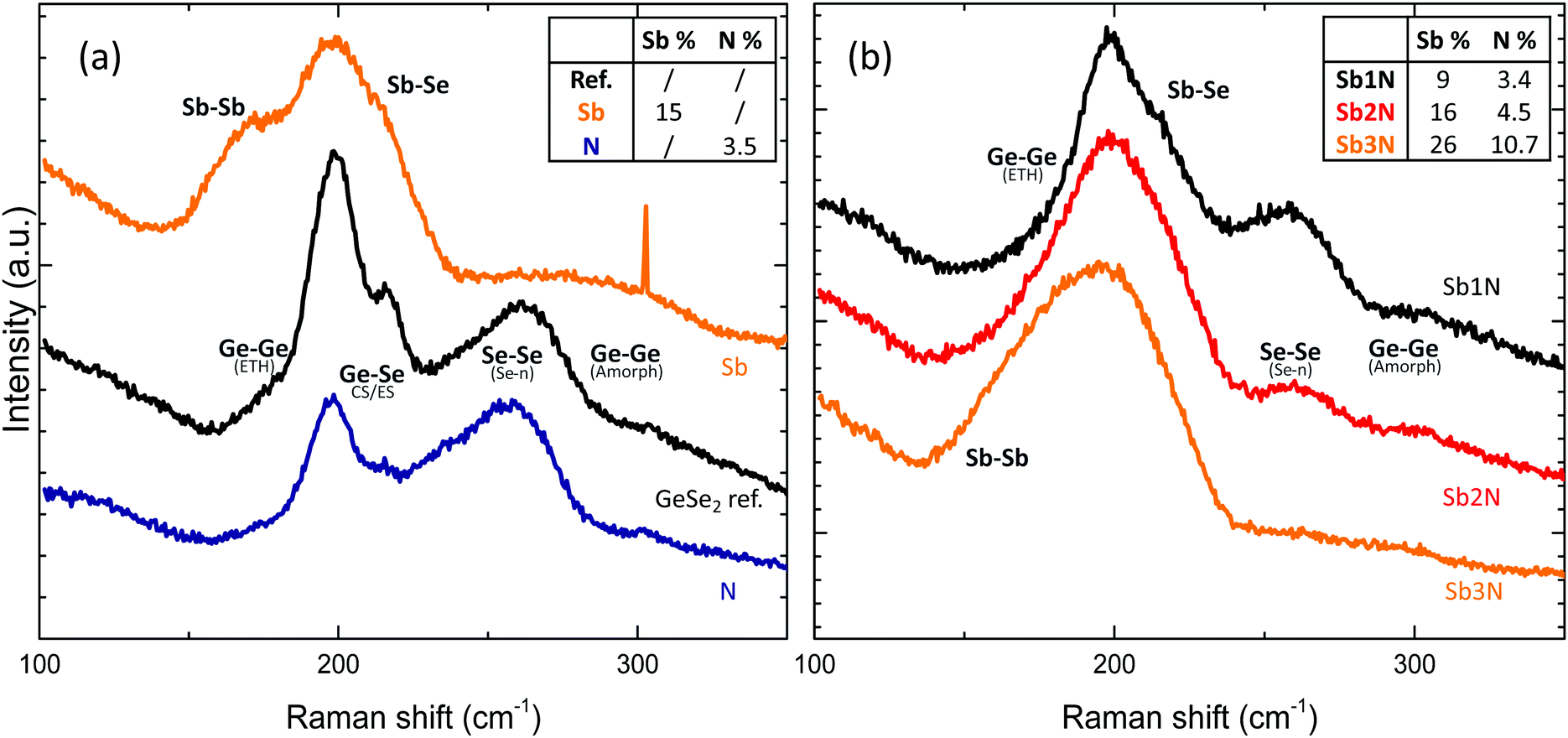
Finally, the impact of doping on bond presence was explored. Two dopants were examined, Sb and N, based on previous work on Se rich Ge–Se materials25,26 as well as theoretical calculations of the bond enthalpy using Pauling's equation27 according to the work of Lankhorst et al.28 which can be found in Table 2. These suggest N has a strong tendency to bond to Ge, while Sb is more attracted to Se thus allowing for a targeted tuning of Ge–Ge and Se–Se bonds. The concentrations of N and Sb are listed in table in the legend of Fig. 10.
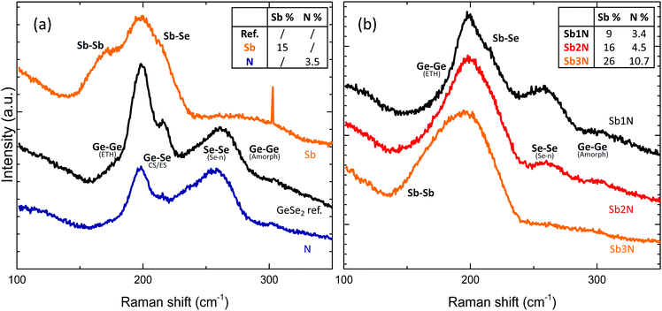 |
| | Fig. 10 Raman spectra of doped GeSe2 layers. (a) Separate doping of Sb and N (b) co-doping of Sb and N. Areas of interest are indicated with the main bonds mode expected in the region.25 | |
The structural units that make up the undoped reference material consist of Ge–Ge, Ge–Se and Se–Se bonds. When adding a medium amount of Sb, the pure Se modes disappear as Se chains are broken and replaced with Sb–Se bonds. These bonds show up in the Raman spectrum at around 220 cm−1 but overlap partially with ES Ge–Se modes. There is also an excess Sb–Sb bonds at 160 cm−1. Notable as well is the appearance of a low intensity broad band which can be attributed to elemental Ge, in agreement with observation of pure Ge and Ge-rich samples. In contrast, addition of N mostly targets the Ge–Ge bonds related to ethane-like Ge2Se3 structural units as Ge will prefer to bond with N rather than itself. Since the Ge–N bond strength is higher than that of Ge–Se bonds as well, some of the Ge–Se bonds are also broken, leading to the formation of more Se–Se bonds in addition to Ge–N bonds. The same was observed from first-principles simulated atomic models of N-doped amorphous GeSe samples.29 This can also be clearly observed from the spectrum as the peaks related to Ge–Se bonds are diminished in favour of the now more intense Se–Se peak. The modes relating to Ge–N16 are expected around 600 cm−1 which was out of the detection range of the setup used. When adding both Sb and N simultaneously, as can be seen in Fig. 10b, a balancing act occurs. The calculated Ge–N bond enthalpy is comparable to that of Sb–N so excess Sb and N will tend to bind with each other. As a result, Ge–Se bonds are kept intact and fewer Sb–Sb bonds are formed. By tuning the amount of Sb, a composition can be obtained which has a minimum of homopolar Sb, Se and Ge bonds. This corresponds to composition labelled Sb2N. Interesting to note is that a further increase of Sb not only increases the Sb–Sb mode intensity but also the concentration of N in the sample. This indicates that a higher Sb content results in a more efficient incorporation of N, further suggesting the Sb attracts N to itself.
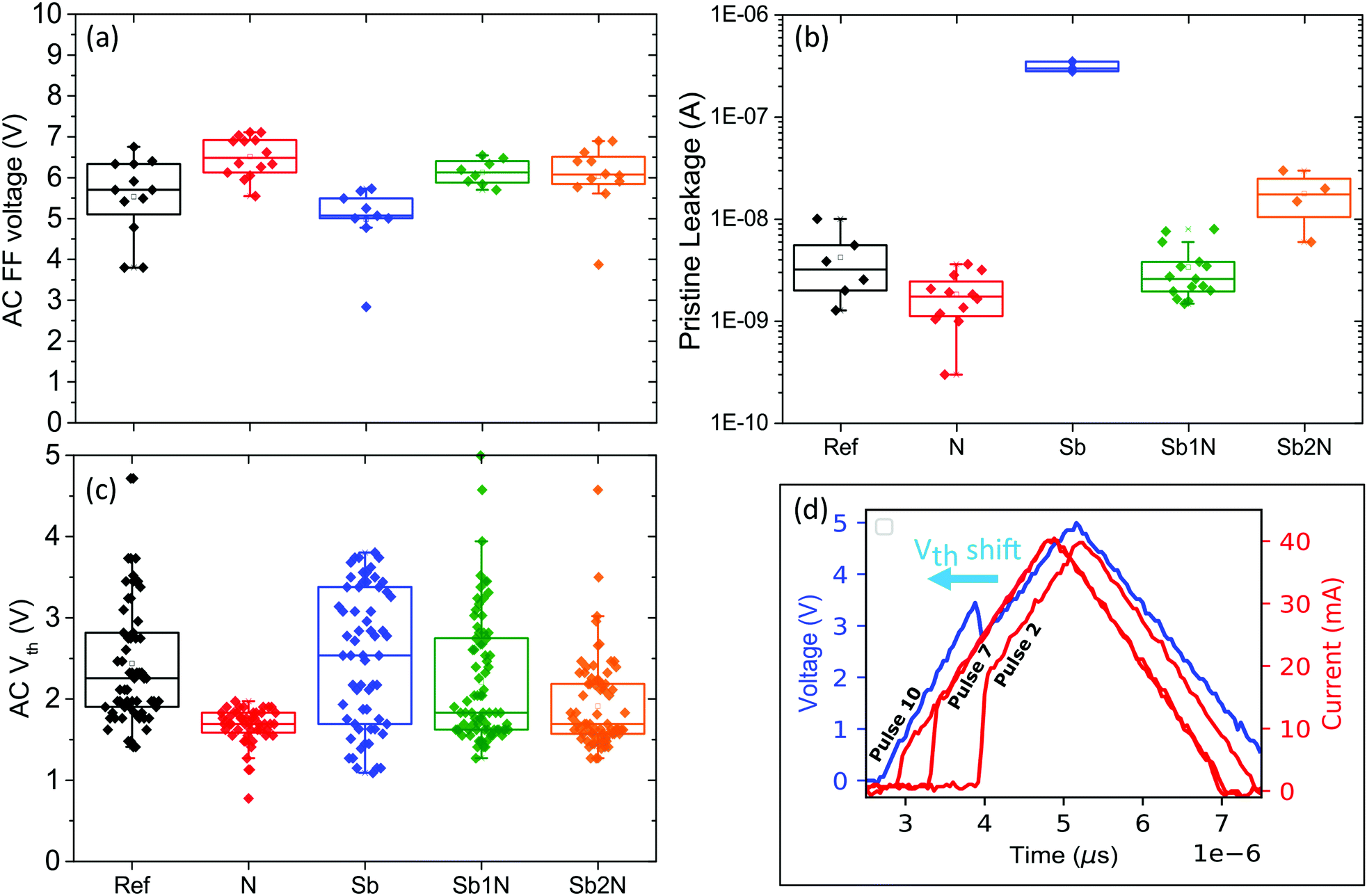
Fig. 11 summarizes the result of the electrical characterization. Compared to the reference, the addition of N increases the VFF. Conversely, the addition of Sb lowers the VFF. For the samples where N and Sb were added together we see a similar balancing act as observed in the Raman spectra. When looking at the pristine leakage the effects are reversed. The addition of N lowers the leakage of GeSe2. From the Raman analysis we can understand this as a larger fraction of the material consists of pure Se–Se bonds and an elimination of Ge–Ge bonds. The addition of a medium amount of Sb greatly increases the pristine leakage. This correlates to the appearance of Sb homopolar bonds as well as Sb–Se bonds, possibly indicating Sb clustering and Sb–Se phases25 which give rise to increased conductivity. The low leakage current can be recovered by adding N. As was also observed in the Raman analysis this prevents the formation of Sb homopolar bonds. When the Sb content is sufficiently low, the presence of N can completely prevent the formation of Sb homopolar bonds and no increase of leakage current is observed. When adding more Sb the leakage current increases slightly but comparing samples Sb to Sb2N which hold nearly the same amount of Sb, the addition of N still greatly limits the leakage current increase. Previous studies have already observed that higher optical band gap OTS materials tend to exhibit higher threshold voltages and lower leakage currents.31,32 The relationship however is not always simple as the density of localized states plays an important role33 as well as the method through which a band gap value is obtained.18 The (optical) band gap was not determined in this paper but previous studies have reported a band gap for GeSe2 thin films in the range of 2.02–2.2 eV.31,34,35 Sb doping has been shown to lower this bandgap value to 1.75–1.4 eV31,35,36 for comparative doping levels. The effects of N doping are dependent on the material composition. For Ge rich materials (50% Ge), N has been shown to increase the band gap33 but can also slightly lower the bandgap for Ge-poor compositions (under 33%).31 The electrical results reported in this paper are thus in agreement with this overall trend, as the composition of the layers is slightly rich in Ge (35%).
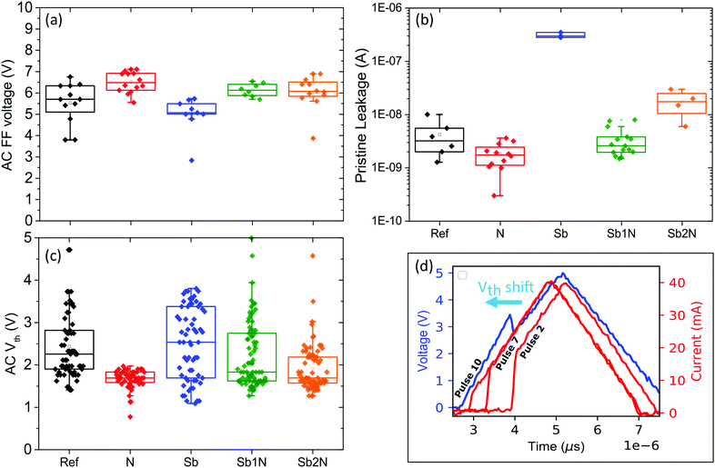 |
| | Fig. 11 (a) First-fire voltage using a 2.5 μs rise and fall time triangular pulse of at least 8 cells (b) Pristine leakage at 2 V prior to first fire (c) Threshold voltage determined from 15 successive 1 μs rise and fall time triangular pulses for 3 to 5 working cells (d) example of Vth shift for Sb1N. | |
The AC threshold voltage Vth was obtained by cycling several cells 15 times and measuring the voltage at which the measured current undergoes a sharp transition. Compared to the first fire voltage it can be observed that for the nitrogen doped sample, the Vth is now the lowest. The Vth was determined as the voltage at which the current undergoes the greatest change. This analysis however does not impose a minimum on the sharpness of the transition. For the N doped sample it was observed that the cells were fairly leaky after first fire, with the conductivity increasing more or less gradually as the applied voltage increases. For these cells, the Vth indicates the point where the rate of change was highest, yet no true threshold switching was observed. This points to some amount of Ge–Ge bonds in these materials being required to create a minimum amount of mobility gap localized states in order to facilitate OTS switching, a result which is supported by ab initio calculations.19,29 For the other samples, sharp threshold switches were observed. For the pure Sb doping the Vth shows a large degree of spread, which is the result of cycle-to-cycle variation with no clear trend. This may the explained by local structural variations of the Sb clusters found in this material which may be reorganizing during cycling. For the Sb and N co-doped samples the spread is reduced. In addition, there is a clear trend in the cycle to cycle variation as demonstrated in Fig. 11d. This plot shows several pulsed IV measurement cycles on the same cell. As the material is cycled, the Vth shifts to lower voltages. For composition Sb2N the shift is smallest and the material quickly approaches a stable Vth of 1.6 V. In addition to being the most electrically stable composition, the materials also has the lowest leakage current after cycling as can be seen in Table 3.
Table 3 Median leakage current at 2 V after 15 cycles
| Ref. |
N |
Sb |
Sb1N |
Sb2N |
| 50 μA |
200 μA |
150 μA |
15 μA |
10 μA |
This indicates that the presence of homopolar bonds may result in decreased electrical stability as the composition with the lowest amount of homopolar bonds, Sb2N, is the most stable. This can be understood as hetero polar bonds are on average stronger as well as more energetically favourable. As a result homopolar bonds are most affected by repeated cycling and will tend to reorganise which induces drift.
4 Conclusions
In this paper we have combined Raman spectroscopic data with electrical characterization to successfully gain a deeper understanding of the relation between bond presence and threshold switching characteristics. A thorough analysis of the base material reveals that sputtered Ge1−xSex films have a high degree of disorder and contain an excess amount of homopolar bonds. Certain Ge–Ge modes were observed that are also present in pure Ge, indicating Ge clustering occurs inside the layer. The impact of annealing, deposition conditions and doping on the bond formation and threshold switching is presented and summarized in Table 4. A correlation can be observed between the presence of Ge–Ge homopolar bonds, particularly those associated with elemental Ge, and increased leakage current. The same holds for Sb–Sb homopolar bond presence. It can also be seen that both excess Se–Se and Ge–Ge homopolar bonds (and Sb in the case of excess Sb doping) can have a negative impact on the electrical stability of the material. Thus, minimizing homopolar bond presence is beneficial to improve the electrical stability of the material. The results regarding N doping and annealing, however, indicate that a certain minimum amount of Ge–Ge bonds is still required to facilitate OTS switching. It is possible to affect the bond structure after deposition. Amongst the methods explored, doping is most effective for this purpose. It is possible to tune bond presence in a targetted fashion by co-doping with Sb and N. A doping level of 15% Sb and 4.5% N can effectively eliminate the majority of Se–Se bonds without increasing the Ge–Ge bond presence or inducing too many additional Sb homopolar bonds. This composition shows low leakage current, the lowest threshold voltage and the highest electrical stability.
Table 4 Summary of the impact of several (post)deposition processes on the bond presence and electrical parameters compared to as-deposited 35% Ge GeSe2. Arrows indicate a increased or decreased presence of bonds
| Process |
Impact on bonds |
Impact on electrical parameters |
| Annealing |
Pure Ge–Ge & Se–Se↓ |
Lower Ipris and higher VFF |
| Ge–Se↑ |
Leaky after FF |
| Increasing pressure |
ETH Ge–Ge↑ |
Higher Ipris and lower VFF |
| Ge–Se↓ |
Minimal impact on Vth |
| Adding Sb |
Se–Se↑ |
Higher Ipris and lower VFF |
| Se–Sb & Sb–Sb↑ |
Large variability |
| Adding N |
Ge–Ge & Ge–Se↓ |
Lower Ipris and higher VFF |
| Se–Se↑ |
Leaky after FF |
| Co–doping Sb + N |
Ge–Ge & Se–Se↓ |
Similar Ipris and lower Vth |
| Sb–N↑ |
Better stability |
Conflicts of interest
There are no conflicts to declare.
Acknowledgements
This research was made possible with the financial support of the BOF-UGent GOA-01G01019 project.
Notes and references
-
D. Reinsel, J. Gantz and J. Rydning, IDC White Paper, 2018 Search PubMed.
- G. W. Burr, M. J. Brightsky, A. Sebastian, H. Cheng, J. Wu, S. Kim, N. E. Sosa, N. Papandreou, H. Lung, H. Pozidis, E. Eleftheriou and C. H. Lam, IEEE Journal on Emerging and Selected Topics in Circuits and Systems, 2016, 6, 146–162 Search PubMed.
-
D. C. Kau, S. Tang, I. V. Karpov, R. Dodge, B. Klehn, J. A. Kalb, J. Strand, A. Diaz, N. Leung, J. Wu, Sean Lee, T. Langtry, Kuo-wei Chang, C. Papagianni, Jinwook Lee, J. Hirst, S. Erra, E. Flores, N. Righos, H. Castro and G. Spadini, 2009 IEEE International Electron Devices Meeting (IEDM), A stackable cross point Phase Change Memory, 2009, pp. 1–4 Search PubMed.
- G. W. Burr, R. S. Shenoy, K. Virwani, P. Narayanan, A. Padilla, B. Kurdi and H. Hwang, J. Vac. Sci. Technol., B: Nanotechnol. Microelectron.: Mater., Process., Meas., Phenom., 2014, 32, 040802 Search PubMed.
- B. Govoreanu, G. L. Donadio, K. Opsomer, W. Devulder, V. V. Afanas'ev, T. Witters, S. Clima, N. S. Avasarala, A. Redolfi, S. Kundu, O. Richard, D. Tsvetanova, G. Pourtois, C. Detavemier, L. Goux and G. S. Kar, Thermally stable integrated Se-based OTS selectors with >20 MA cm−2 current drive, >3.103 half-bias nonlinearity, tunable threshold voltage and excellent endurance, Symposium on VLSI Technology, 2017, 92–T9392 Search PubMed.
- P. Němec, S. Zhang, V. Nazabal, K. Fedus, G. Boudebs, A. Moréac, M. Cathelinaud and X.-H. Zhang, Opt. Express, 2010, 18, 22944–22957 CrossRef.
- M. Olivier, P. Němec, G. Boudebs, R. Boidin, C. Focsa and V. Nazabal, Opt. Mater. Express, 2015, 5, 781–793 CrossRef.
- E. Baudet, C. Cardinaud, A. Girard, E. Rinnert, K. Michel, B. Bureau and V. Nazabal, J. Non-Cryst. Solids, 2016, 444, 64–72 CrossRef CAS.
- R. Zhang, J. Ren, H. Jain, Y. Liu, Z. Xing and G. Chen, J. Am. Ceram. Soc., 2014, 97, 1421–1424 CrossRef CAS.
- R. Pan, H. Tao, H. Zang, X. Zhao and T. Zhang, J. Alloys Compd., 2009, 484, 645–648 CrossRef CAS.
- T. Ikari, T. Tanaka, K. Ura, K. Maeda, K. Futagami and S. Shigetomi, Phys. Rev. B: Condens. Matter Mater. Phys., 1993, 47, 4984 CrossRef CAS.
- T. Edwards and S. Sen, J. Phys. Chem. B, 2011, 115, 4307–4314 CrossRef CAS.
- P. Boolchand and W. Bresser, Philos. Mag. B, 2000, 80, 1757–1772 CrossRef CAS.
-
Y.-L. Gan and L. Wang, Ninth International Symposium on Precision Engineering Measurement and Instrumentation, Analysis of Raman spectra of GeAsSe glass using different peak-fitting method, 2015, p. 94461V Search PubMed.
- K. Jackson, A. Briley, S. Grossman, D. V. Porezag and M. R. Pederson, Phys. Rev. B: Condens. Matter Mater. Phys., 1999, 60, R14985 CrossRef CAS.
- I. Chambouleyron and A. Zanatta, J. Appl. Phys., 1998, 84, 1–30 CrossRef CAS.
- M. Wihl, M. Cardona and J. Tauc, J. Non-Cryst. Solids, 1972, 8, 172–178 CrossRef.
-
N. S. A. Valery Afanasev, L. Goux, G. S. Kar, M. Houssa and A. Stesmans1, 49th IEEE Semiconductor Interface Specialists Conference, Electron States in Ovonic Switching GexSe1−x(0.4 < x < 0.72) Films, 2018 Search PubMed.
- S. Clima, D. Garbin, K. Opsomer, N. S. Avasarala, W. Devulder, I. Shlyakhov, J. Keukelier, G. L. Donadio, T. Witters, S. Kundu, B. Govoreanu, L. Goux, C. Detavernier, V. Afanas'ev, G. S. Kar and G. Pourtois, Phys. Status Solidi RRL, 2020, 14, 1900672 CrossRef CAS.
- R. Flasck and H. K. Rockstad, J. Non-Cryst. Solids, 1973, 12, 353–356 CrossRef CAS.
- S. Roychowdhury, M. Samanta, S. Perumal and K. Biswas, Chem. Mater., 2018, 30, 5799–5813 CrossRef CAS.
- Q. Yan, H. Jain, J. Ren, D. Zhao and G. Chen, J. Phys. Chem. C, 2011, 115, 21390–21395 CrossRef CAS.
- F. Verger, V. Nazabal, F. Colas, P. Němec, C. Cardinaud, E. Baudet, R. Chahal, E. Rinnert, K. Boukerma and I. Péron,
et al.
, Opt. Mater. Express, 2013, 3, 2112–2131 CrossRef.
- S. Rossnagel, I. Yang and J. Cuomo, Thin Solid Films, 1991, 199, 59–69 CrossRef CAS.
-
A. Verdy, G. Navarro, V. Sousa, P. Noe, M. Bernard, F. Fillot, G. Bourgeois, J. Garrione and L. Perniola, IEEE International Memory Workshop (IMW), 2017, pp. 1–4 Search PubMed.
-
N. S. Avasarala, B. Govoreanu, K. Opsomer, W. Devulder, S. Clima, C. Detavernier, M. van der Veen, J. Van Houdt, M. Henys, L. Goux and G. S. Kar, 47th European Solid-State Device Research Conference (ESSDERC), Doped {GeSe} materials for selector applications, 2017, pp. 168–171 Search PubMed.
-
L. Pauling, The Nature of the Chemical Bond…, Cornell university press, Ithaca, NY, 1960, vol. 260 Search PubMed.
- M. Lankhorst, J. Non-Cryst. Solids, 2002, 297, 210–219 CrossRef CAS.
-
S. Clima, B. Govoreanu, K. Opsomer, A. Velea, N. S. Avasarala, W. Devulder, I. Shlyakhov, G. L. Donadio, T. Witters, S. Kundu, L. Goux, V. Afanasiev, G. S. Kar and G. Pourtois, IEEE International Electron Devices Meeting (IEDM), 2017, pp. 4.1.1–4.1.4.
- J. R. Chelikowsky and J. Phillips, Phys. Rev. B: Solid State, 1978, 17, 2453 CrossRef CAS.
- P. Noe, A. Verdy, F. DAcapito, J.-B. Dory, M. Bernard, G. Navarro, J.-B. Jager, J. Gaudin and J.-Y. Raty, Sci. Adv., 2020, 6, eaay2830 CrossRef CAS.
- Y. Koo and H. Hwang, Sci. Rep., 2018, 8, 1–7 CrossRef.
- H.-W. Ahn, D. Seok Jeong, B.-K. Cheong, H. Lee, H. Lee, S.-D. Kim, S.-Y. Shin, D. Kim and S. Lee, Appl. Phys. Lett., 2013, 103, 042908 CrossRef.
- Z. Černošek, E. Černošková, M. Hejdová, J. Holubová and R. Todorov, J. Non-Cryst. Solids, 2017, 460, 169–177 CrossRef.
- T. Halenkovič, J. Gutwirth, P. Němec, E. Baudet, M. Specht, Y. Gueguen, J.-C. Sangleboeuf and V. Nazabal, J. Am. Ceram. Soc., 2018, 101, 2877–2887 CrossRef.
- Z. Zhen-Ying, C. Fen, L. Shun-Bin, W. Yong-Hui, S. Xiang, D. Shi-Xun and N. Qiu-Hua, Chin. Phys. B, 2015, 24, 066801 CrossRef.
Footnote |
| † Electronic supplementary information (ESI) available. See DOI: 10.1039/d0tc04086j |
|
| This journal is © The Royal Society of Chemistry 2021 |
Click here to see how this site uses Cookies. View our privacy policy here. 
 a,
Karl
Opsomer
b,
Thomas
Nuytten
b,
Stefanie
Sergeant
b,
Wouter
Devulder
b,
Sergiu
Clima
b,
Ludovic
Goux
b,
Gouri Sankar
Kar
b and
Christophe
Detavernier
*a
a,
Karl
Opsomer
b,
Thomas
Nuytten
b,
Stefanie
Sergeant
b,
Wouter
Devulder
b,
Sergiu
Clima
b,
Ludovic
Goux
b,
Gouri Sankar
Kar
b and
Christophe
Detavernier
*a