Formation and properties of iodine- and acetonitrile-functionalized two-dimensional Si materials: a Density Functional Theory study†
Dimitrios
Kaltsas
 ,
Panagiotis
Pappas
 and
Leonidas
Tsetseris
 *
*
Department of Physics, National Technical University of Athens, Heroon Polytechniou 9 Zographou Campus, 15780, Athens, Greece. E-mail: leont@mail.ntua.gr
First published on 7th December 2021
Abstract
Topotactic transformations of suitable layered three-dimensional precursors are among the most robust methods to prepare two-dimensional (2D) materials based on silicon or germanium. Here we use Density Functional Theory calculations to probe the mechanisms underlying the formation of 2D-Si sheets functionalized with iodine atoms (SiI) or acetonitrile molecules [Si(MeCN)] starting from a layered CaSi2 precursor. We identify the sequence of exothermic surface reactions that enable the adsorption of, not only iodine atoms, but, surprisingly, also of solvent acetonitrile molecules on both sides of the top layer of a Si-terminated CaSi2 surface and its ensuing exfoliation as a standalone 2D sheet. In the acetonitrile case, the as-formed 2D material exhibits intriguing structural and electronic properties with an unusual quasi-one-dimensional substructure of silicon chains and a Dirac-like cone in the energy band diagram. The results elucidate the atomic-scale details of the established experimental technique of topotactic synthesis of functionalized silicene and identify new structural motifs for 2D materials.
Introduction
Following the isolation of graphene,1 a major task has been to synthesize 2D materials compatible with the current semiconductor industry where silicon has the leading role. Suitable candidates are group-IV elements, namely Si, Ge and Sn with their respective 2D forms known as silicene, germanene and stanene.2–4 In their pure forms (i.e. without chemical functionalization) freestanding silicene and germanene films are predicted by theory to form slightly buckled structures with a mixture of sp2 and sp3 hybridization.5,6 Experimentally, however, both silicene and germanene have only been realized on top of suitable substrates (e.g. Ag, Au, Ir).2,7While unmodified Si freestanding monolayer sheets are highly reactive, chemical modification can lead to the formation of stable 2D films as the unsaturated bonds become passivated. Functionalized Si films can be synthesized via a top-down approach that involves processing of calcium disilicide (CaSi2), a suitable 3D layered precursor wherein Ca atoms are intercalated between 2D buckled silicene layers.8 Deintercalation of Ca atoms can be achieved via topochemical reactions with HCl (the so called Wöhler synthesis)9 leading to the formation of layered Si crystals known as siloxene [SiH6(OH)3]10–14 or polysilane (Si6H6).12,13,15 Several Density Functional Theory (DFT) studies have investigated the structural and electronic properties of various types of 2D Si sheets functionalized with, e.g., hydrogen,14,16–19 halogens,18–21 and alkali metals,22,23 or with larger moieties such as hydroxyl,19 methyl,18,19 naphthyl/anthracyl,24 phenyl,25,26 hydrocarbon27 groups and others.2,28 In all these DFT studies, the 2D Si-based films were predicted to be semiconductors with band gaps covering a wide range of values from 0.26 eV to 2.5 eV. Based on these values, silicene derivatives are, in principle, suitable for applications such as photovoltaics, photodetectors, light-emitting diodes, and lasers.2 Recent experimental studies29–33 have also highlighted their potential as anodes for lithium-ion batteries29 and as biocompatible and biodegradable materials in cancer phototherapy.30,31 Intriguingly, these recent studies have suggested that freestanding silicene sheets without chemical modification can be synthesized via topochemical reactions of CaSi2 in a mixture of I2 and acetonitrile (CH3CN), also known as methyl cyanide (MeCN), at room temperature.29–33
In this work, we employed extensive DFT calculations to probe the atomic scale mechanisms that underlie the topochemical synthesis of functionalized silicene sheets starting from a CaSi2 precursor, with a focus on reactions in the presence of iodine and acetonitrile molecules. By doing that we have for the first time, to our knowledge, unravelled the series of exothermic reactions that give as exfoliated products Si-monolayers fully functionalized with iodine (in the following we use the symbol SiI for this 2D material) and 2D sheets of calcium diiodide (CaI2). By the same token, we have found that full functionalization of silicene can occur also with acetonitrile molecules, even though the latter are typically regarded as relatively inert solvent species. The most stable structure of 2D sheets with acetonitrile functionalization [hereafter, we denote them as Si(MeCN)] comprises one-dimensional chains of Si atoms which are linked through pairs of acetonitrile anchors. The configuration is interesting not only because of this uncommon structural 2D arrangement, but also in terms of its electronic properties associated with the presence of small gaps and Dirac-like cones in the corresponding energy band diagram.
Methodology
Calculations for structural relaxations and electronic properties were performed with the Vienna Ab initio Simulation Package (VASP) software34 and an energy cutoff of 400 eV for the plane wave basis. The interactions between valence electrons and ionic cores were described with projector augmented waves (PAW),35 while exchange and correlation effects were accounted for through the Perdew–Burke–Ernzerhof (PBE) generalized-gradient approximation (GGA) functional, unless stated otherwise.36 Sampling of reciprocal space in total energy calculations was performed with the Monkhorst–Pack37 method, whereas the tetrahedron method38 was employed for summations in k-space to obtain the electronic densities of states (DOS). The sizes of the k-point grids were 12 × 12 × 1 (4 × 4 × 1) for the primitive cell (supercell) calculations, 8 × 6 × 1 for the fully functionalized Si(MeCN) sheets and 2 × 1 × 1 for the CaSi2 slab supercell. van der Waals interactions were included through the DFT-D3 method.39 For calculations on 2D materials and slabs, a vacuum of at least 20 Å was added in the z-direction to essentially eliminate interactions between periodic images. Ab initio molecular dynamics (AIMD) simulations were performed in a 2 × 2 × 1 supercell of the most stable Si(MeCN) polymorph using a Nosé–Hoover thermostat in the canonical ensemble (NVT).Results
In this work we used DFT calculations to study the interactions between freestanding silicene monolayers or CaSi2 crystals with iodine and acetonitrile molecules. The following two subsections present the results for the freestanding films and CaSi2 surfaces, respectively.Iodine and acetonitrile adsorption on silicene
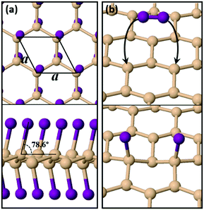
Pure silicene is a 2D allotrope of Si with a lattice parameter of 3.86 Å, a slightly buckled configuration of 0.45 Å (height difference between the two inequivalent atoms in the primitive cell) and a Si–Si bond length of 2.28 Å. Our results on the structural details of silicene are in excellent agreement with previous pertinent theoretical studies.5,6 Previous theoretical work has shown that functionalization of silicene with iodine (or other halogens) leads to the formation of stable 2D sheets with different possible geometries,20,21 the most stable of which is the so-called chair conformation shown in Fig. 1(a). Compared to pure silicene, SiI shows larger buckling at 0.68 Å, larger Si–Si bond lengths of 2.45 Å and a lattice parameter of 4.06 Å. The vertical distance between two I atoms of opposing sides is 5.53 Å, which is very close to the experimentally measured thickness (6.00 Å) of monolayer films synthesized from CaSi2 crystals in the presence of I2 in acetonitrile.29 A notable feature of the structure is that the I atoms are not situated directly above or below the respective Si atoms to which they are bonded. As can be observed in the side view of Fig. 1(a), each I atom tilts at an angle of 76.8° relative to the horizontal plane of the film. We have found that it is this tilt which enhances the dynamic stability of the system by rendering all frequencies real in the corresponding phonon band diagram of Fig. S1 (ESI†). The material is stable also under strain with a well-defined and unique energy minimum, as shown in Fig. S2 (ESI†).In terms of the electronic properties, Fig. S3 (ESI†) shows the electronic band structure of SiI for different strain levels along two vertical directions in the sheet, including the pristine case of the unstrained material. SiI is predicted to be a narrow-gap semiconductor with a direct band gap of 0.87 eV at the Γ point of the Brillouin zone. Calculations with the hybrid HSE06 exchange–correlation functional45 widen the gap to 1.58 eV, while calculations based on the PBE046 xc-functional find a gap of 2.21 eV. By applying strain, the electronic properties of the material can be tuned further, as is demonstrated by the respective band structure diagrams of Fig. S3 (ESI†). A wide range of gap values can be achieved, ranging from 0.41 eV to 0.95 eV, while the direct/indirect nature of the band gap changes when strain is applied along the a axis.
For freestanding silicene to become fully functionalized as shown in Fig. 1(a), it must react exothermically with I2 molecules. We modelled the interaction of an isolated I2 molecule on an orthogonal 15.45 Å × 13.38 Å silicene supercell. We found that the molecule dissociates spontaneously (i.e. with no energy barrier) and its iodine atoms become adatoms on Si sites which are second neighbors as shown in Fig. 1(b). The absence of a reaction barrier and the strong energy gain of 1.81 eV shows that the functionalization of silicene with I species is a very efficient process.
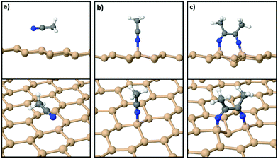
On the other hand, the interaction of various organic molecules with silicene has been studied in previous theoretical works24,40–44 in relation to band gap engineering, molecule detection, energy storage and energy conversion. With respect to acetonitrile, however, to the best of our knowledge, there is only one DFT study40 which probed just the physisorption of MeCN on silicene. Using the orthogonal 15.45 Å × 13.38 Å silicene supercell we confirmed40 that the most stable geometry of an isolated acetonitrile molecule is a physisorbed configuration wherein it lies parallel to the silicene sheet as shown in Fig. 2(a). The adsorption energy for the physisorbed state is 0.27 eV per MeCN molecule within the DFT-D3 approximation. On the other hand, the chemisorbed configuration of Fig. 2(b) for a molecule anchored to silicene through a N–Si bond has a lower adsorption energy of 0.16 eV, confirming that an isolated MeCN molecule is relatively inert.
However, when a second acetonitrile molecule is added to the system the situation changes drastically with the energy preference flipping in favor of a chemisorbed state. Fig. 2(c) shows the relaxed structure with two MeCN molecules bonded to the freestanding film. The N ends of each of the two molecules bind to two second-nearest Si neighbors on silicene, and a C–C bond (1.52 Å) is formed between them. The CH3 groups of the protruding MeCN molecules point away from each other and form angles of about 120.0°, as expected for an sp2 hybridization scheme. Through this reaction, the system gains an overall energy of 0.42 eV per MeCN with respect to a geometry where both MeCN molecules are physisorbed as in Fig. 2(a).
In contrast to SiI wherein each I atom binds to a single Si atom, we found that the N atom of a MeCN molecule can form either one or two bonds to Si atoms. This in turn leads to different extended geometries with full functionalization. In the most stable configuration (Type 1) depicted in Fig. 3, all N atoms are three-fold coordinated and all Si atoms are four-fold coordinated. The a and b lattice parameters are 4.25 Å and 11.44 Å, respectively. In this structure, the hexagonal bonding network of the original silicene sheet is broken and Si atoms form buckled linear chains parallel to the a crystal axis. Adjacent Si chains are held together through N–Si bonds by the N atoms of the MeCN molecules. We stress that this type of quasi-one-dimensional substructure is uncommon for 2D materials derived so far through functionalization of honeycomb lattices. Acetonitrile dimers are aligned along the b axis, but they tilt away from the vertical position in an alternate fashion (Fig. 3). We define the tilt angle as the angle between the horizontal plane of the film and the plane that passes through N–C bonds of each dimer. AIMD simulations for a time interval of 2 ps at temperatures 300 K, 600 K, and 1000 K confirm that the Si(MeCN) polymorph of Fig. 3 remains intact even at high temperatures (i.e. 1000 K). The corresponding animation files can be found in the ESI† (Movies S1–S3).
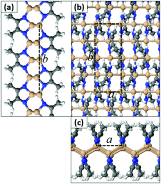 | ||
| Fig. 3 (a and c) Side views and (b) top view of the Type 1a Si(MeCN) 2D sheet. The dashed lines represent the primitive cell (Si: orange, N: blue, C: gray, H: white spheres). | ||
Interestingly, we have identified two such stable configurations (with real vibrational frequencies at the Γ point) whose tilt angles and energies differ, respectively, by only 5° and 0.5 meV per unit cell. Their band structure diagrams are shown in Fig. 4 (for the structure of Fig. 3, we term it Type 1a) and Fig. S4 (ESI†) (Type 1b). Both polymorphs have small direct band gaps (0.08 eV for 1a and 0.23 eV for 1b) at the Γ point with Dirac-like cones which are more prevalent for the Type 1a structure. The projected DOS plots (that of 1a is given in Fig. 5, the one for 1b is similar) show that the main contributions to the valence and conduction bands come from the s and p orbitals of Si and the p orbitals of N and C. Calculations with the hybrid HSE06 xc-functional of the eigenenergies at band edges give gaps of 0.06 eV and 0.29 eV for, respectively, Type 1a and 1b. When strain (up to 1%) is applied to 1a the gap is slightly modified between 0.07 eV and 0.14 eV, as is depicted in the corresponding band diagrams of Fig. S5 (ESI†). Moreover, as is shown in Fig. S6 (ESI†), Type 1 structures are stable under applied strains of up to 3%.
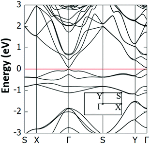 | ||
| Fig. 4 Electronic band structure of the Type 1a Si(MeCN) sheet. The valence band maximum is set to 0 eV and the inset shows the first Brillouin zone and corresponding high symmetry points. | ||
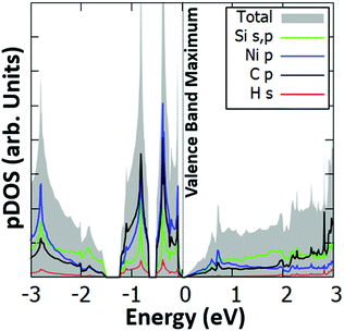 | ||
| Fig. 5 Projected electronic density of states (pDOS) for the s orbitals of Si and H, and the p orbitals of Si, N and C of the Type 1a Si(MeCN) sheet. The valence band maximum is set to 0 eV. | ||
Fig. S7(a) (ESI†) shows another polymorph (Type 2) which is less stable than Type 1 by 0.12 eV per Si atom. This structure is similar to Type 1 in terms of bonding, but differs in that its MeCN dimes do not tilt away from the upright position with respect to the horizontal backbone of the 2D sheet. Moreover, because of the alternate tilting pattern described above, the unit cell of Type 1 is twice the size of that of Type 2 along the b-axis. Fig. S7(b) and S8(a) (ESI†) show the next two most stable polymorphs (Type 3 and Type 4) whose energies are 0.37 eV per Si higher than those of Type 1. In Type 3, half of the N atoms are two-fold coordinated and the rest are three-fold coordinated, while all Si atoms have four bonds. We have also identified another three possible conformations (Types 5–7) shown in Fig. S8 and S9 (ESI†). The structure of Type 3 resembles the Type 1 geometry on one side (N atoms have three bonds), while the other side is akin to the Type 2 configuration with two-fold coordinated N atoms. In Types 5–7 all N atoms bind to a single Si atom on the hexagonal silicon sheet. They differ in how the C–C bonds in the MeCN dimers are oriented above and below the silicene-like network. Types 5–7 are significantly less stable by 0.65–0.74 eV per Si atom compared to Type 1. The relative stabilities and structural properties of all polymorphs are summarized in Table S1 (ESI†).
The electronic DOS for Types 2–7 are given in Fig. S10 (ESI†) and the corresponding band gap values are also summarized in Table S1 (ESI†). At the PBE-GGA level, Types 3 and 7 are metallic, Type 2 is a semiconductor with a very small gap of 0.07 eV and Types 4–6 are also semiconductors but with slightly large band gaps in the range 0.30–0.62 eV. Calculations with the HSE06 functional45 widen the gaps to 0.54–1.31 eV.
In terms of the energies for the synthesis of fully functionalized SiI or Si(MeCN) with respect to freestanding silicene and free I2 or MeCN molecules, the reactions can be described by the equation:
 | (1) |
Topochemical reactions of CaSi2 with iodine or acetonitrile
In order to assess the possibility of synthesizing SiI and Si(MeCN), we studied how a CaSi2 crystal reacts with I2 and acetonitrile molecules. CaSi2 is a 3D layered crystal with a trigonal structure of group symmetry R![[3 with combining macron]](https://www.rsc.org/images/entities/char_0033_0304.gif) m.8 The calculated PBE-GGA values for the a and c lattice parameters (respectively, 3.84 Å and 15.84 Å) are in excellent agreement with the experimental values.8
m.8 The calculated PBE-GGA values for the a and c lattice parameters (respectively, 3.84 Å and 15.84 Å) are in excellent agreement with the experimental values.8
To model the Ca- and Si-terminated CaSi2 surfaces, we simulated slabs with at least 20 Å of vacuum in the z-direction using the theoretically predicted lattice parameters of bulk CaSi2. The supercell consisted of 6 atomic layers in total (3 Ca and 3 Si) and the atoms of the bottom layer were kept fixed during relaxation. The unit cells are highlighted with the dashed lines in Fig. 6. The most stable geometries for the Si-terminated surface are similar to the case of freestanding silicene, resembling the chair conformation for SiI and forming dimers in the case of MeCN molecules. The Ca-terminated surface passivated with iodine resembles the trigonal structure of CaI2, and in the case of acetonitrile the MeCN molecules form dimers through a C–C bond similar to the Si-terminated surface. In addition, we find that both Ca- and Si-terminated surfaces react exothermically with iodine and acetonitrile. To calculate the energy gained through these reactions we used the following equation:
 | (2) |
 is the total energy of a CaSi2 supercell with n adsorbed I atoms or MeCN molecules,
  is the total energy of the bare supercell (without I or MeCN) and Efreemol is ½ of the total energy of a free I2 molecule or the total energy of a free MeCN molecule respectively. The energy gain (per I atom or per MeCN molecule) for the Ca surface is 2.72 eV (1.89 eV) for I atoms (MeCN molecules), while for the Si surface the energy gain is calculated at 1.14 eV (1.12 eV) for I atoms (MeCN molecules) with all values suggesting that CaSi2 surfaces tend to react readily with both I2 and MeCN.
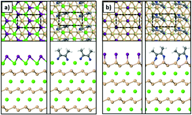 | ||
| Fig. 6 The (a) Ca-terminated and (b) Si-terminated surfaces of a CaSi2 crystal passivated with iodine or acetonitrile (Ca: green, Si: orange, I: purple, N: blue, C: gray, H: white spheres). | ||
Experimentally, during the chemical treatment of CaSi2 (e.g. with aqueous HCl11 or I2 in acetonitrile29) Ca atoms are gradually deintercalated from the material when the crystal is left long enough in the solution. In order to reach complete deintercalation and achieve the synthesis of the fully functionalized SiI or Si(MeCN) sheets, these processes must progress towards the bulk of the material from the exposed surfaces of the crystals, with I2 or MeCN molecules inserted between the Ca and Si layers. The results discussed in the previous paragraph showed that reactions of iodine or acetonitrile with the (001) surface of CaSi2 crystals are exothermic processes. Here, we look further into how these reactions progress within the material from an exposed CaSi2 side surface. To simulate the slab, we used an orthogonal supercell of dimensions 7.68 Å × 26.61 Å × 15.84 Å (along the x, y and z directions respectively) with six atomic layers (three Ca and three Si) and an added 20 Å of vacuum in the y and z axes as depicted in Fig. S11 (ESI†). The top surface was Si-terminated and the atoms of the bottom Ca layer were kept fixed during relaxations to simulate the bulk of the material. The total number of atoms in the bare supercell were 48 Ca and 96 Si atoms and the energy released during successive reactions was calculated according to eqn (2).
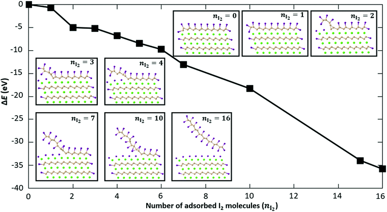
Fig. 7 shows the change in energy as more and more I2 molecules are adsorbed on the CaSi2 slab. The zero of energy is taken to be the total energy of the fully passivated slab as shown in the inset of Fig. 7 for nI2 = 0. Extra I2 molecules are gradually inserted from the side between the top Si layer and the Ca layer underneath. The relaxed structures for some representative cases are shown in the insets of Fig. 7. As more I2 molecules are added to the system, the top Si layer is gradually detached and iodine is adsorbed also on the bottom side of the Si sheet. Simultaneously, the exposed Ca layer gets passivated by iodine atoms that assume positions of the trigonal CaI2 crystal, similar to what is observed for the Ca-terminated surface [Fig. 6(a)]. All adsorption steps are found to be exothermic. In the final configuration (nI2 = 16) the top Si layer has been completely functionalized with iodine and becomes detached from the surface of the crystal. The fact that there is no energy penalty in our calculations serves as a theoretical proof of principle that CaSi2 crystals can react with iodine to produce fully functionalized Si. It is well known that similar topochemical reactions occur in the hydrogenation of silicene or germanene47–50 and in other materials as well,51,52 but, to our knowledge, this is the first time that the atomic details of these transformations are elucidated with first principles calculations. We should also note that we tested the effect a proximal solvent acetonitrile molecule may have on the exothermic insertion of iodine atoms and found it to be minimal. In particular, for the step that adds a second iodine pair in Fig. 7 the reaction energy is 4.32 eV. This is to be compared to the value of 4.20 eV obtained without this MeCN molecule. The fact that the two values are so close to each other suggests that the presence of solvent molecules does not alter significantly the energetics of I-functionalization we analyzed above.
After the removal of the top layer in the form of a functionalized Si sheet, the CaSi2 crystal is left with an exposed iodinated Ca-terminated surface. Using the orthogonal cell of the bare Ca-terminated surface depicted in Fig. 6(a), we show that successive reactions with iodine can also lead to the removal of the top Ca layer in the form of CaI2. The relaxed structures and total energy change ΔE per cell (eqn (2)) are given in Fig. S12 (ESI†). It turns out that it is favorable for iodine to react with Ca atoms and produce a CaI2 layer that is very weakly bound to the Si layer beneath it, both for the unpassivated [Fig. S12(c), ESI†] and the fully passivated case [Fig. S12(d), ESI†]. In this manner, the reaction cycle of Fig. 7 is reset and the process may progress to the next Si layer until the whole crystal is deintercalated leading to the synthesis of SiI. Notably, the same topotactic reaction leads to the formation of a second 2D material, namely CaI2 films53–56 as shown in Fig. S12(d) (ESI†). This is an important finding as it provides an alternative and straightforward route for the synthesis of two-dimensional CaI2.
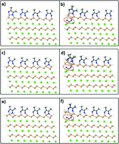
On the other hand, in order to synthesize Si sheets fully functionalized with acetonitrile, MeCN molecules should adsorb exothermically on both sides of the Si surface sheet. To investigate this reaction, we used a model of a CaSi2 slab where, in this case, Si atoms on the edges of the crystal are passivated with H atoms on the exposed sides as shown in Fig. 8(a). Fig. 8(b) shows the relaxed configuration of the same supercell with an extra MeCN molecule positioned between the top two layers. We compared the total energy of this final configuration to the sum of the total energy of Fig. 8(a) plus a free MeCN molecule (to conserve the total number of atoms) and it turns out that Fig. 8(b) is less stable by 0.97 eV. We also tested different levels of passivation for the CaSi2 crystals [Fig. 8(c–f)] with and without an inserted MeCN molecule and the respective energy differences are 1.97 eV and 2.33 eV. Because of this first endothermic step, the insertion of acetonitrile molecules in-between the layers of a CaSi2 crystal and, concomitantly, the complete topotactical synthesis of 2D-Si(MeCN) will require annealing at elevated temperatures, possibly in the range of 200–500 °C. The quantitative estimate of the activation energy and temperature requires, of course, a much more involved and large-scale simulation which goes beyond the scope of the present study.
Conclusions
Using DFT calculations we probed the atomic-scale details of the topochemical reactions of iodine and acetonitrile molecules with freestanding silicene and CaSi2 crystals. We demonstrated that I2 species react with the crystal surfaces to produce fully passivated SiI films and that all relevant reaction steps are exothermic. Furthermore, we identified novel 2D Si sheets functionalized with acetonitrile that include narrow-gap semiconductors and metals, adding new functional members in the family of 2D forms of silicon. Given the rich possibilities with respect to the choice of solvents and/or oxidants (e.g. I2, HCl) in the topochemical deintercalation of CaSi2, our results serve as a proof of principle that more complex structures of 2D Si can be synthesized by combining different molecules that form bonds not just with the Si sheet, but also with each other.Conflicts of interest
There are no conflicts to declare.Acknowledgements
This research was funded in the context of the project “Modern two-dimensional nanomaterials for state-of-the-art technological applications” (MIS 5049431) under the call for proposals “Researchers' support with an emphasis on young researchers- 2nd Cycle”. The project is co-financed by Greece and the European Union (European Social Fund – ESF) by the Operational Programme Human Resources Development, Education and Lifelong Learning 2014–2020. The work used computational resources of the Greek Research & Technology Network (GRNET) in the National HPC facility – ARIS – under project pr009016.Notes and references
- K. S. Novoselov, A. K. Geim, S. V. Morozov, D. Jiang, Y. Zhang, S. V. Dubonos, I. V. Grigorieva and A. A. Firsov, Science, 2004, 306, 666–669 CrossRef CAS PubMed.
- S. M. Spencer and T. Morishita, Silicene: Structure, Properties and Applications, Springer International Publishing, 1st edn, 2016 Search PubMed.
- J. C. Garcia, D. B. de Lima, L. V. C. Assali and J. F. Justo, J. Phys. Chem. C, 2011, 115, 13242–13246 CrossRef CAS.
- F.-f. Zhu, W.-j. Chen, Y. Xu, C.-l. Gao, D.-d. Guan, C.-h. Liu, D. Qian, S.-C. Zhang and J.-f. Jia, Nat. Mater., 2015, 14, 1020–1025 CrossRef CAS.
- K. Takeda and K. Shiraishi, Phys. Rev. B: Condens. Matter Mater. Phys., 1994, 50, 14916–14922 CrossRef CAS PubMed.
- D. Kaltsas and L. Tsetseris, Phys. Chem. Chem. Phys., 2013, 15, 9710–9715 RSC.
- M. E. Dávila and G. Le Lay, Sci. Rep., 2016, 6, 20714 CrossRef.
- S. Dick and G. Öhlinger, Z. Kristallogr. - New Cryst. Struct., 1998, 213, 246 Search PubMed.
- F. Wöhler, Justus Liebigs Ann. Chem., 1863, 127, 257–274 CrossRef.
- H. Kautsky, Z. Anorg. Allg. Chem., 1921, 117, 209–242 CrossRef.
- A. Weiss, G. Beil and H. Meyer, Z. Naturforsch., B: Anorg. Chem., Org. Chem., 1980, 35, 25–30 CrossRef.
- J. R. Dahn, B. M. Way, E. Fuller and J. S. Tse, Phys. Rev. B: Condens. Matter Mater. Phys., 1993, 48, 17872–17877 CrossRef CAS PubMed.
- U. Dettlaff-Weglikowska, W. Hönle, A. Molassioti-Dohms, S. Finkbeiner and J. Weber, Phys. Rev. B: Condens. Matter Mater. Phys., 1997, 56, 13132–13140 CrossRef CAS.
- A. Atsalakis and L. Tsetseris, J. Phys.: Condens. Matter, 2014, 26, 285301 CrossRef PubMed.
- S. Yamanaka, H. Matsu-ura and M. Ishikawa, Mater. Res. Bull., 1996, 31, 307–316 CrossRef CAS.
- M. Houssa, E. Scalise, K. Sankaran, G. Pourtois, V. V. Afanas’ev and A. Stesmans, Appl. Phys. Lett., 2011, 98, 223107 CrossRef.
- D. Kaltsas, T. Tsatsoulis, O. G. Ziogos and L. Tsetseris, J. Chem. Phys., 2013, 139, 124709 CrossRef CAS PubMed.
- E. Zaminpayma and P. Nayebi, Phys. E, 2016, 84, 555–563 CrossRef CAS.
- P. A. Denis, Phys. Chem. Chem. Phys., 2015, 17, 5393–5402 RSC.
- N. Gao, W. T. Zheng and Q. Jiang, Phys. Chem. Chem. Phys., 2012, 14, 257–261 RSC.
- W.-B. Zhang, Z.-B. Song and L.-M. Dou, J. Mater. Chem. C, 2015, 3, 3087–3094 RSC.
- T. H. Osborn and A. A. Farajian, J. Phys. Chem. C, 2012, 116, 22916–22920 CrossRef CAS.
- T. Hussain, S. Chakraborty, A. De Sarkar, B. Johansson and R. Ahuja, Appl. Phys. Lett., 2014, 105, 123903 CrossRef.
- M. D. Brennan, T. Morishita and M. J. S. Spencer, J. Chem. Phys., 2016, 144, 114704 CrossRef PubMed.
- R. Wang, X. Pi, Z. Ni, Y. Liu and D. Yang, RSC Adv., 2015, 5, 33831–33837 RSC.
- J. Dai and X. C. Zeng, Phys. Chem. Chem. Phys., 2015, 17, 17957–17961 RSC.
- P. Rubio-Pereda and N. Takeuchi, J. Chem. Phys., 2013, 138, 194702 CrossRef.
- A. Nayad, S. K. Hnawi, A. Hasnaoui, L. E. Firdoussi and M. A. Ali, Mater. Today: Proc., 2021, 39, 1103–1117 CAS.
- J. Liu, Y. Yang, P. Lyu, P. Nachtigall and Y. Xu, Adv. Mater., 2018, 30, 1800838 CrossRef PubMed.
- C. He, L. Yu, L. Ding, H. Yao, Y. Chen and Y. Hao, Biomaterials, 2020, 255, 120181 CrossRef CAS PubMed.
- H. Lin, W. Qiu, J. Liu, L. Yu, S. Gao, H. Yao, Y. Chen and J. Shi, Adv. Mater., 2019, 31, 1903013 CrossRef PubMed.
- F. Wang, H. Duan, R. Zhang, H. Guo, H. Lin and Y. Chen, Nanoscale, 2020, 12, 17931–17946 RSC.
- H. Duan, H. Guo, R. Zhang, F. Wang, Z. Liu, M. Ge, L. Yu, H. Lin and Y. Chen, Biomaterials, 2020, 256, 120206 CrossRef CAS PubMed.
- G. Kresse and J. Furthmüller, Phys. Rev. B: Condens. Matter Mater. Phys., 1996, 54, 11169–11186 CrossRef CAS.
- G. Kresse and D. Joubert, Phys. Rev. B: Condens. Matter Mater. Phys., 1999, 59, 1758–1775 CrossRef CAS.
- J. P. Perdew, K. Burke and M. Ernzerhof, Phys. Rev. Lett., 1996, 77, 3865–3868 CrossRef CAS PubMed.
- D. J. Chadi and M. L. Cohen, Phys. Rev. B: Solid State, 1973, 8, 5747–5753 CrossRef.
- P. E. Blöchl, O. Jepsen and O. K. Andersen, Phys. Rev. B: Condens. Matter Mater. Phys., 1994, 49, 16223–16233 CrossRef.
- S. Grimme, J. Antony, S. Ehrlich and H. Krieg, J. Chem. Phys., 2010, 132, 154104 CrossRef PubMed.
- T. P. Kaloni, G. Schreckenbach and M. S. Freund, J. Phys. Chem. C, 2014, 118, 23361–23367 CrossRef CAS.
- R. Stephan, M.-C. Hanf and P. Sonnet, J. Chem. Phys., 2015, 143, 154706 CrossRef PubMed.
- R. Stephan, M.-C. Hanf and P. Sonnet, Phys. Chem. Chem. Phys., 2015, 17, 14495–14501 RSC.
- N. Gao, G. Y. Lu, Z. Wen and Q. Jiang, J. Mater. Chem. C, 2017, 5, 627–633 RSC.
- V. O. Vo, T. L. Pham and V. A. Dinh, Mater. Trans., 2020, 61, 1449–1454 CrossRef CAS.
- A. V. Krukau, O. A. Vydrov, A. F. Izmaylov and G. E. Scuseria, J. Chem. Phys., 2006, 125, 224106 CrossRef PubMed.
- C. Adamo and V. Barone, J. Chem. Phys., 1999, 110, 6158 CrossRef CAS.
- H. Nakano, M. Ishii and H. Nakamura, Chem. Commun., 2005, 2945–2947 RSC.
- H. Nakano, Y. Sugiyama, T. Morishita, M. J. S. Spencer, I. K. Snook, Y. Kumai and H. Okamoto, J. Mater. Chem. A, 2014, 2, 7588–7592 RSC.
- H. Nakano, J. Ceram. Soc. Jpn., 2014, 122, 748–754 CrossRef.
- E. Bianco, S. Butler, S. Jiang, O. D. Restrepo, W. Windl and J. E. Goldberger, ACS Nano, 2013, 7, 4414–4421 CrossRef CAS PubMed.
- L. Tsetseris, Nanoscale, 2016, 8, 13558–13561 RSC.
- L. Tsetseris, FlatChem, 2017, 2, 49–53 CrossRef CAS.
- M. Baskurt, M. Yagmurcukardes, F. M. Peeters and H. Sahin, J. Chem. Phys., 2020, 152, 164116 CrossRef CAS PubMed.
- F. Lu, W. Wang, X. Luo, X. Xie, Y. Cheng, H. Dong, H. Liu and W.-H. Wang, Appl. Phys. Lett., 2016, 108, 132104 CrossRef.
- G. Bhattacharyya, P. Garg, P. Bhauriyal and B. Pathak, ACS Appl. Nano Mater., 2019, 2, 6152–6161 CrossRef CAS.
- X.-F. Chen, L. Wang, Z.-Y. Zeng, X.-R. Chen and Q.-F. Chen, Philos. Mag., 2020, 100, 1982–2000 CrossRef CAS.
Footnote |
| † Electronic supplementary information (ESI) available. See DOI: 10.1039/d1cp03442a |
| This journal is © the Owner Societies 2022 |

