
Strain-induced enhancement in the electronic and thermal transport properties of the tin sulphide bilayer†
Shagun
Nag
 a,
Ranber
Singh
b and
Ranjan
Kumar
*ca
a,
Ranber
Singh
b and
Ranjan
Kumar
*ca
aDepartment of Physics, Panjab University, Chandigarh, India. E-mail: ranjan@pu.ac.in
bDepartment of Physics, Sri Guru Gobind Singh College, Chandigarh, India
cPhysics Department, Faculty of Science, King Abdulaziz University, P. O. Box 80203, Jeddah 21589, Saudi Arabia
First published on 27th November 2021
Abstract
The enhancement in the thermoelectric figure of merit (ZT) of a material is limited by the interplay between the electronic transport coefficients. Here we report the greatly enhanced thermoelectric performance of the SnS bilayer with the application of isotropic strain, due to the simultaneous increase in the Seebeck coefficient and low lattice thermal conductivities. Based on first-principles calculations combined with Boltzmann transport theory, we predict that the band structure of the SnS bilayer can be effectively tuned using the strain, and the Seebeck coefficient is significantly improved for the tensile strain. The lattice thermal conductivities for the bilayer under the tensile strain are quite low (0.21–1.89 W m−1 K−1 at 300 K) due to the smaller frequencies of the acoustic phonon modes. Along the zigzag (armchair) direction, the room temperature peak ZT value of 4.96 (2.40) is obtained at a strain of 2% (4%), which is 5.3 (2.03) times higher than the peak ZT of the unstrained bilayer along the zigzag (armchair) direction. Thus the strain-tuned SnS bilayer is a good thermoelectric material with low lattice thermal conductivities and promising ZT values at room temperature.
1 Introduction
Despite the advancements in green energy generation techniques, approximately two-third of the energy generated across the globe is wasted as unwanted heat.1 Thermoelectric (TE) materials, which are capable of converting this unwanted heat directly into electrical energy based on the Seebeck effect,2 have been extensively investigated over the past few decades.3,4 The performance and efficiency of a TE material are expressed in terms of its dimensionless figure of merit,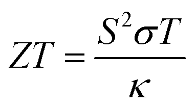 , where S is the Seebeck coefficient, σ is the electrical conductivity, T is the absolute temperature, and κ is the thermal conductivity which includes the electronic (κe) and lattice (κl) contributions. For a thermoelectric material to be used for practical applications, one would favour a high power factor (PF), which is defined as S2σ, and a low thermal conductivity (κ). However, the intrinsic correlation and coupling among the physical parameters (S, σ, and κe) makes it difficult to improve the ZT value of TE materials.5 For instance, an increase in the carrier concentration increases the σ, while it also lowers the Seebeck coefficient.6 In addition, an increase in σ leads to a comparable increase in κe since σ and κe are related by the Wiedmann–Franz law: κe = LσT, where L = 2.45 × 10⁻⁸ W Ω K−2 is the Lorentz number for free electrons.7
Many approaches have been proposed to tune the TE performance,8,9 such as nanostructuring,10 doping,11 band engineering,12 carrier concentration optimization,13 making superlattice structures,14 and so on. In particular, nanostructured low-dimensional materials show great potential in the TE conversion efficiency due to the simultaneous enhancement in the power factor and the reduction in the thermal conductivity (κ).15
Recently, remarkable progress has been made in the study of two-dimensional (2D) materials owing to the flexibility in tuning their electronic properties by changing the number of layers with respect to their bulk counterparts.16,17 2D monochalcogenides, including SnSe, SnS, GeSe and GeS, have also been explored greatly for thermoelectric applications.18–21 The interest in exploring their promising applications in the thermoelectrics field has been widely evoked since one of their bulk counterparts, the SnSe single crystal, is reported to have an ultralow lattice thermal conductivity, lower than 0.25 W m−1 K−1, at a temperature greater than 800 K and a high ZT of 2.6 ± 0.3 at 923 K.22,23 In addition, Sn-based chalcogenides are non-toxic, earth-abundant and eco-friendly in nature,24 which makes them better candidates for large-scale and commercial applications compared with lead-based chalcogenides,25 which are toxic in nature.
For the SnSe monolayer, a peak ZT value of 3.27 at 700 K has been predicted,18 which is 7 times the ZT value of the corresponding bulk phase. In the case of 2D SnS2, it has been found that σ and κ are negatively correlated and the ZT value can be enhanced by reducing the thickness of SnS2.26 Shafique et al. predicted high figures of merit for SnSe (ZT = 2.63, and 2.46), SnS (ZT = 1.75, and 1.88), GeSe (ZT = 1.99, and 1.73), and GeS (ZT = 1.85, and 1.29) at 700 K along the armchair and zigzag directions, respectively.27 The TE properties of 2D transition metal dichalcogenides such as MoS2, MoSe2, WS2 and WSe2 have also been found to be enhanced due to the near degeneracies of their conduction and valence band valleys.28,29 It is well known that a high valley degeneracy in the electron band structure leads to better thermoelectric properties since it simultaneously leads to a high Seebeck coefficient and a high σ value due to the enhanced density of states.30 This fact has stimulated attempts to engineer 2D thermoelectric materials to obtain the convergence of different valleys by doping or applying external strain.31–34 Strain-engineering has been proved as a facile and effective way of tuning the physical properties of 2D materials.35 Strain can be easily induced in practice via lattice mismatch between the substrate and the sheet deposited over it, or by distortion of the nanostructures.
Strain-engineering of 2D materials has resulted in the reduction of their lattice thermal conductivities, for example, the room-temperature κl value of monolayer PtSe2 can be decreased by about 60% under 4% biaxial tensile strain,31 and similar behaviour has also been shown in the ZrS232 and ZrSe236 monolayers. In addition, strain is also an effective way to improve the electrical transport properties, for example, in the case of phosphorene37 and puckered antimonene,38 where the application of in-plane strain enhances the mobilities of the charge carriers in a particular direction, which results in enhanced values of the power factors. Many studies about the effect of strain on the thermoelectric properties of monochalcogenides have been reported.39 However, due to the presence of van der Waals (vdW) interactions among the layers in chalcogenide materials, monochalcogenides tend to form bilayer structures. Moreover, compared with the monolayer structures, some 2D bilayer structures like phosphorene and MoS2 exhibit more striking properties due to their smaller band gaps than in the single-layer structures.40,41 This implies that 2D bilayer structures provide more opportunities for tuning the band gap via strain. These unique electronic properties in bilayer structures stimulated us to explore and tune the TE properties of bilayer SnS using strain engineering.
Here in this work, we systematically studied the strain effect on the electronic and transport properties of the SnS bilayer using first-principles density functional theory (DFT) and semi-classical Boltzmann transport theory. For the bilayer, our calculations reveal that the application of tensile strain enhances the Seebeck coefficient whereas the application of compressive strain reduces the Seebeck coefficient. The lattice thermal conductivities of the bilayer show lower values for the tensile strain compared with the compressive strain case. Consequently, the figure of merit shows higher values for the tensile strain compared with the compressive strain cases. The rest of the paper is organized as follows: in Section 2, we discuss the computational details; the results are discussed in detail in Section 3; and finally, the results are summarized in Section 4.
2 Computational details
The present calculations include three parts. First, the DFT and the plane-wave pseudopotential formulations42,43 as implemented in the Quantum ESPRESSO package44 are used to calculate the structural and electronic properties of the SnS bilayer material. A kinetic energy cutoff of 80 Ry is employed for the plane wave (PW) basis, and the exchange–correlation energy is described by the generalized gradient approximation (GGA) using the Perdew–Burke–Ernzerhof (PBE) functional.45 Considering the underestimation of the band gap from the PBE functional, we employed the Heyd–Scuseria–Ernzerhof (HSE06)46 functional with 25% Fock exchange to predict a more accurate band gap of the bilayer. A series of in-plane isotropic strains ranging from −10% to 10% are imposed to the SnS bilayer. The strains are defined as ε = (l − l0)/l0 × 100%, where l and l0 are the lattice constants with and without strain, respectively. The conjugate gradient (CG) algorithm is used for the geometrical optimization of the strained bilayers until the forces on the atoms are converged to 10−6 Ry Å−1 and the total energy is converged to 10−8 Ry using the Monkhorst–Pack47k-mesh of 16 × 15 × 1. The DFT Grimme-D2 vdW48 interactions have been explicitly included for optimization of the bilayer structures. The vacuum thickness of 15 Å is adopted to avoid interactions between the bilayer and its images perpendicular to the plane. The formation energies per formula unit cell (ΔEf) of the SnS bilayer under different strains are calculated using the expression49| ΔEf = [E(SnS)2Dbi − nE(Sn)atom − nE(S)atom]/2n, | (1) |
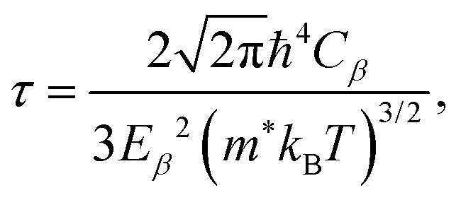
Second, based on the obtained electronic band structure, the electronic transport coefficients, i.e., the Seebeck coefficient S, the electrical conductivity with the relaxation time σ/τ, and the electron thermal conductivity with the relaxation time κe/τ, are calculated using the BoltzTraP code,50 which is based on the semi-classical Boltzmann transport theory under a constant relaxation time (τ) and with rigid band approximations. The relaxation time of the charge carriers is estimated using the deformation potential theory.51 Within this theory, the relaxation time of the charge carriers is defined as52,53
 | (2) |
 . Using the τ value computed using density functional theory, we calculated values of σ and κe at different temperatures.
Third, for the phonon dispersion calculations, we use the finite displacement method as implemented in the Phonopy package.55 For the calculation of 2nd order harmonic interatomic force constants (IFCs), we use a 5 × 5 × 1 supercell containing 200 atoms. The phonon thermal conductivity (κl) is calculated by solving the linearized phonon Boltzmann transport equation (LBTE) as implemented in the Phono3py package.56 The Phono3py package solves the LBTE under the single-mode-relaxation-time (SMRT) method. The LBTE method of calculating the κl value has been widely used in the literature for simple crystals like SnSe, GeSe, etc.27
In general, the κl value, when expressed in terms of the phonon velocity operator,57 has contributions from the populations and coherence distribution terms. The LBTE approach calculates contributions only from the population terms to the total κl value, whereas the unified theory includes contributions from both population and coherence terms to the total κl. In the case of simple crystals, the main contribution to κl is from the population terms, hence the calculated κl values using the LBTE approach are quite accurate.56,58,59 However, in the case of complex crystals, there is a major contribution from the coherence term to κl and hence the calculated κl values from the LBTE and unified theory show major differences.60 However, our SnS system is also a simple crystal like SnSe, GeSe, etc., and thus we expect that there will not be much difference between the calculated κl values using the LBTE approach and unified theory. So, we have used the LBTE approach for the calculation of κl in our work. Finally, using the calculated S, σ, κe and κl values, the thermoelectric performance of the SnS bilayer subjected to different isotropic strains is calculated in terms of the dimensionless figure of merit (ZT).
3 Results and discussion
Bulk SnS crystallizes in the layered orthorhombic structure with the crystallographic symmetry of D2h,16 which belongs to the no. 62 space group. Because of the presence of weak van der Waals interactions among the layers, it is possible to exfoliate a few layers from the bulk structure. In our work, we have taken a bilayer structure out from the optimized structure of the bulk SnS system. Fig. 1 shows the top and side view structures of the optimized SnS bilayer along the zigzag and armchair directions. The optimized lattice constants are a = 4.02 Å and b = 4.36 Å along the zigzag and armchair directions, which are in reasonable agreement with previous reports (a = 4.02 Å and b = 4.34 Å).16 To study the impact of weak van der Waals (vdW) interactions among the layers of the bilayer on its properties, we calculate the thickness of the bilayer with and without including the vdW interactions in our study. The thickness of the bilayer decreases from 8.52 Å (without vdW correction) to 8.38 Å (with vdW correction), which suggests that the weak interactions among the layers could have a significant effect on the properties of the bilayer. Furthermore, in order to apply the isotropic strain in the SnS bilayer system, the lattice constants along the zigzag and armchair directions are either stretched (or compressed) for studying the effect of tensile (or compressive) strain.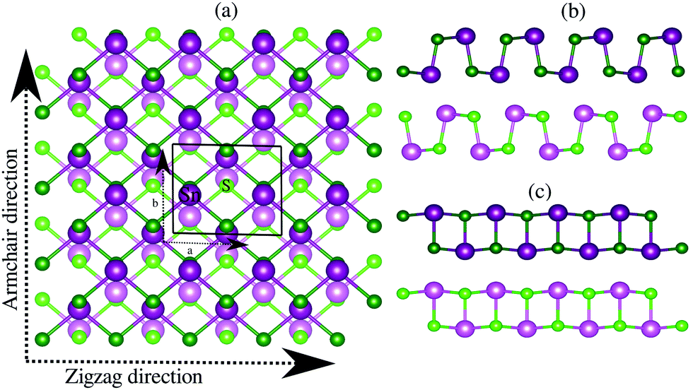 | ||
| Fig. 1 (a) Top view, (b) side view perpendicular to the zigzag direction and (c) side view perpendicular to the armchair direction of the optimized crystal structure of the SnS bilayer. To make the two layers differentiable in the top view, the atoms in the upper (lower) layer are represented with darker (lighter) colors. | ||
To confirm the chemical stability of the SnS bilayer under different strains, the formation energies per formula unit (ΔEf) were calculated and the results are listed in Table 1. The calculated formation energies are found to be negative, which accounts for the chemical stability of the SnS bilayer under different strains. The dynamic stability of the strained bilayer systems is confirmed by computing their phonon spectra as shown in Fig. 2. No imaginary frequency is found within the strain range of −4% to 8%, indicating the dynamic stability of the bilayer within this strain range. In the phonon spectra, 24 dispersion modes are demonstrated, including 21 optical modes and 3 acoustical modes (in-plane transverse TA, in-plane longitudinal LA and out-of-plane ZT). Furthermore, to demonstrate the thermal stability of the strained bilayer systems at room temperature, we performed ab initio molecular dynamics simulations using a 3 × 3 × 1 supercell (shown in Fig. S1 of the ESI†). The simulated results shows that the geometry of the strained bilayer systems remains invariant after heating for 10 picoseconds, which confirms the thermal stability of these systems.
| Strain (%) | ΔEf (eV) | Zigzag | Armchair | E g (eV) |
|---|---|---|---|---|
| C β (× 109 N m−2) | C β (× 109 N m−2) | |||
| −4 | −18.84 | 142.92 | 51.49 | 0.47 |
| −2 | −18.88 | 117.19 | 32.27 | 0.80 |
| 0 | −18.88 | 96.74 | 34.75 | 1.12 |
| 2 | −18.84 | 79.39 | 28.29 | 1.39 |
| 4 | −18.76 | 66.34 | 30.19 | 1.57 |
| 6 | −18.64 | 52.62 | 23.21 | 1.59 |
| 8 | −18.52 | 38.45 | 8.74 | 1.50 |
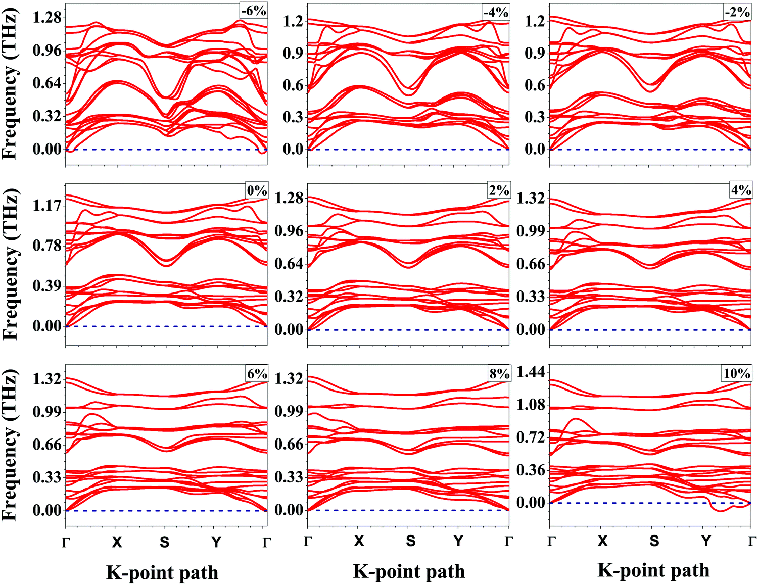 | ||
| Fig. 2 Phonon dispersion curves along the high symmetry k-point paths in the first Brillouin zone for the SnS bilayer under different isotropic strains. The positive phonon frequencies in the strain range of −4% to 8% confirm the dynamic stability of the bilayer within this range. | ||
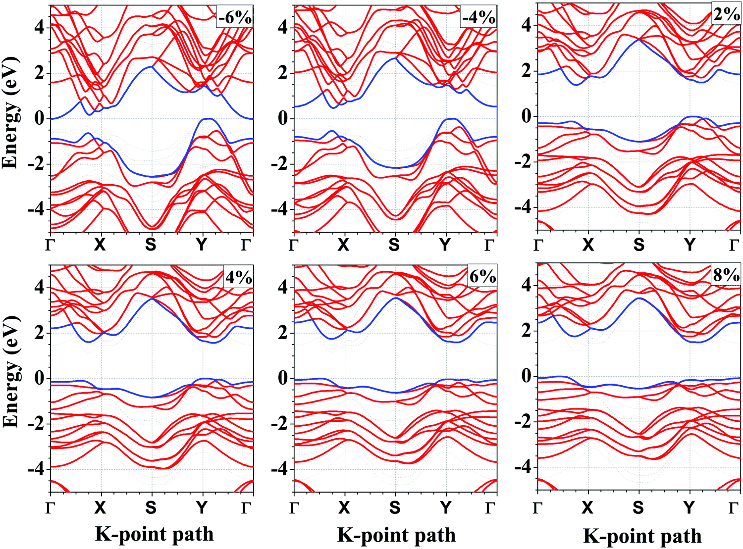
Next, we calculate the PBE band gap of the bilayer with and without considering the effect of vdW interactions. The band gap of the bilayer decreases from 1.19 eV (without vdW interactions) to 1.12 eV (with vdW interactions), which accords well with the result that the thickness of the bilayer decreases when we include the vdW corrections. Furthermore, the PBE band gap of 1.12 eV under the vdW interactions is in good agreement with the previously reported PBE band gap of 1.03 eV.61 Since, the PBE functional underestimates the band gap, we repeated the band structure calculations using the HSE06 functional (shown in Fig. 4(a)). The band gap of the unstrained bilayer under HSE06 correction is 1.63 eV, which is quite close to the previously reported band gap of 1.62 eV under HSE06 correction.16 The valence band maximum (VBM) is located at a k-point along the Y–Γ path and the conduction band minimum (CBM) is located at a k-point along the Γ–X path. Interestingly, the band structure exhibits a “pudding-mould” feature62,63 because the bands along the X–Y direction are flat, meaning large band effective mass values, and the bands along the Γ–X and Y–Γ directions are dispersive, meaning a low band effective mass. This type of band structure leads to a high Seebeck coefficient (S) and a high electrical conductivity (σ), which in turn will lead to a high power factor (S2σ). With the introduction of strain in the system, the band structures, as well as the energy gaps, are significantly affected. The application of compressive strain leads to a decrease in the band gap of the bilayer, and when the compressive strain is large enough, i.e., −6%, the semiconductor-to-metal transition occurs (Fig. 4). The reason for this transition is that with the increase in compressive strain, the interatomic repulsive forces increase and the electronic localization becomes weak, which leads to strengthening of the interatomic orbital interactions, making the valence and conduction bands more dispersive across the Fermi level.64 As a result, the band gap becomes small and the semiconductor-to-metal transition occurs at large compressive strains. Under tensile strain, the band gap increases linearly up to 6% strain and a turnover is presented above this strain value (Fig. 4).
With the electronic band structure of the unstrained bilayer as a reference (black lines), the band structure of the SnS bilayer at different strains (red colour) is plotted in Fig. 3 with the VBM shifted to 0 eV. Under tensile strain, the conduction band shifts up with respect to the valence band, and under compressive strain, the conduction band moves down with respect to the valence band. Furthermore, the band dispersion is also altered under the strain. The VBM and CBM could become sharper under compressive strain, which leads to a smaller effective mass and higher charge-carrier mobilities (Table 2). In the case of tensile strain, the VBM and CBM could become flat, which will lead to a large effective mass and hence smaller charge-carrier mobilities (Table 2). It is also important to note that the strain also induces band convergence in the electronic band structure. Convergent CBMs emerge when the bilayer is under a tensile strain of 2% and 4%, whereas convergent VBMs emerge when the bilayer is under a tensile strain of 6%. Such band convergences are beneficial for improving the performance of thermoelectric materials.65,66
 | ||
| Fig. 3 Electronic band structure of the SnS bilayer under different isotropic strains. The red colour represents the bands of the strained bilayer and the black colour represents the bands of the unstrained bilayer. The blue colour represents the valence band maximum (VBM) and conduction band minimum (CBM) of the strained bilayer systems. The VBM is shifted to 0 eV for reference. | ||
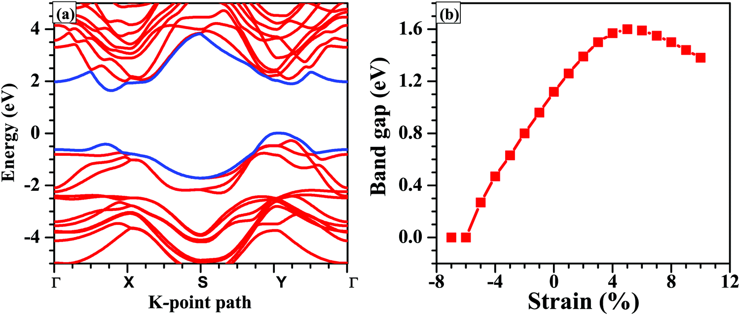 | ||
| Fig. 4 (a) Calculated electronic band structure of the unstrained bilayer including HSE06 correction, and (b) variation of the band gap (using PBE functional) of the SnS bilayer as a function of the applied isotropic strain. At the strain of −6%, the SnS bilayer tends to be a metal and the semiconductor-to-metal transition takes place. | ||
| Charge carrier (direction) | Strain (%) | E β (eV) | m* (m0) | τ (10−14 s) | μ (102 cm2 V−1 s−1) | ||||
|---|---|---|---|---|---|---|---|---|---|
| 300 K | 500 K | 700 K | 300 K | 500 K | 700 K | ||||
| Electron (zigzag) | −4 | 2.44 | 0.12 | 199.07 | 92.49 | 55.83 | 291.68 | 135.56 | 81.84 |
| −2 | 3.02 | 0.15 | 83.31 | 38.72 | 23.37 | 97.69 | 45.40 | 27.41 | |
| 0 | 3.14 | 0.18 | 331.39 | 154.02 | 92.98 | 323.81 | 150.49 | 90.85 | |
| 2 | 3.32 | 0.22 | 152.65 | 70.94 | 42.83 | 122.04 | 56.72 | 34.24 | |
| 4 | 10.58 | 0.26 | 11.37 | 5.28 | 3.19 | 7.69 | 3.57 | 2.16 | |
| 6 | 10.09 | 0.31 | 7.98 | 3.71 | 2.24 | 4.53 | 2.10 | 1.27 | |
| 8 | 9.34 | 0.36 | 0.41 | 0.19 | 0.12 | 0.20 | 0.09 | 0.06 | |
| Hole (zigzag) | −4 | 15.06 | 0.14 | 26.42 | 12.28 | 7.41 | 33.19 | 15.42 | 9.31 |
| −2 | 14.52 | 0.20 | 27.55 | 12.81 | 7.73 | 24.23 | 11.26 | 6.80 | |
| 0 | 13.46 | 0.28 | 7.92 | 3.68 | 2.22 | 4.97 | 2.31 | 1.40 | |
| 2 | 12.64 | 0.42 | 22.61 | 10.51 | 6.34 | 9.47 | 4.40 | 2.66 | |
| 4 | 11.54 | 0.70 | 6.14 | 2.85 | 1.72 | 1.54 | 0.72 | 0.43 | |
| 6 | 6.41 | 1.14 | 12.97 | 6.03 | 3.64 | 2.01 | 0.93 | 0.56 | |
| 8 | 6.08 | 1.08 | 1.91 | 0.89 | 0.53 | 0.31 | 0.14 | 0.09 | |
| Electron (armchair) | −4 | 8.25 | 2.61 | 6.27 | 2.91 | 1.76 | 0.42 | 0.20 | 0.12 |
| −2 | 7.31 | 2.93 | 3.91 | 1.82 | 1.10 | 0.23 | 0.11 | 0.06 | |
| 0 | 6.86 | 0.26 | 24.86 | 11.55 | 6.98 | 16.82 | 7.82 | 4.72 | |
| 2 | 6.49 | 0.41 | 14.19 | 6.60 | 3.98 | 6.09 | 2.83 | 1.71 | |
| 4 | 5.44 | 0.39 | 19.59 | 9.10 | 5.50 | 8.83 | 4.10 | 2.48 | |
| 6 | 5.30 | 0.44 | 12.74 | 5.92 | 3.58 | 5.09 | 2.37 | 1.43 | |
| 8 | 5.61 | 15.98 | 0.26 | 0.12 | 0.07 | 0.003 | 0.002 | 0.0008 | |
| Hole (armchair) | −4 | 10.36 | 0.25 | 20.14 | 9.36 | 5.65 | 14.17 | 6.59 | 3.98 |
| −2 | 10.00 | 0.14 | 16.01 | 7.44 | 4.49 | 20.11 | 9.35 | 5.64 | |
| 0 | 9.02 | 0.53 | 6.33 | 2.94 | 1.78 | 2.10 | 0.98 | 0.59 | |
| 2 | 8.35 | 0.08 | 18.46 | 8.58 | 5.18 | 40.58 | 18.86 | 11.39 | |
| 4 | 7.55 | 0.26 | 6.52 | 3.03 | 1.83 | 4.41 | 2.05 | 1.24 | |
| 6 | 3.45 | 0.21 | 19.71 | 9.16 | 5.53 | 16.51 | 7.67 | 4.63 | |
| 8 | 2.99 | 2.16 | 1.79 | 0.83 | 0.50 | 0.14 | 0.07 | 0.04 | |
The projected electronic density of states of the SnS bilayer at different strains is presented in Fig. 5. The VBM has a contribution mainly due to the p-orbitals of S-atoms, and the CBM has a contribution mainly due to the p-orbitals of Sn-atoms, and the same trend is followed at all strain values. Furthermore, with the increase in the applied tensile strain to the bilayer, there is a significant enhancement in the contribution of the s-orbitals of the Sn-atoms to the VBM of the bilayer.
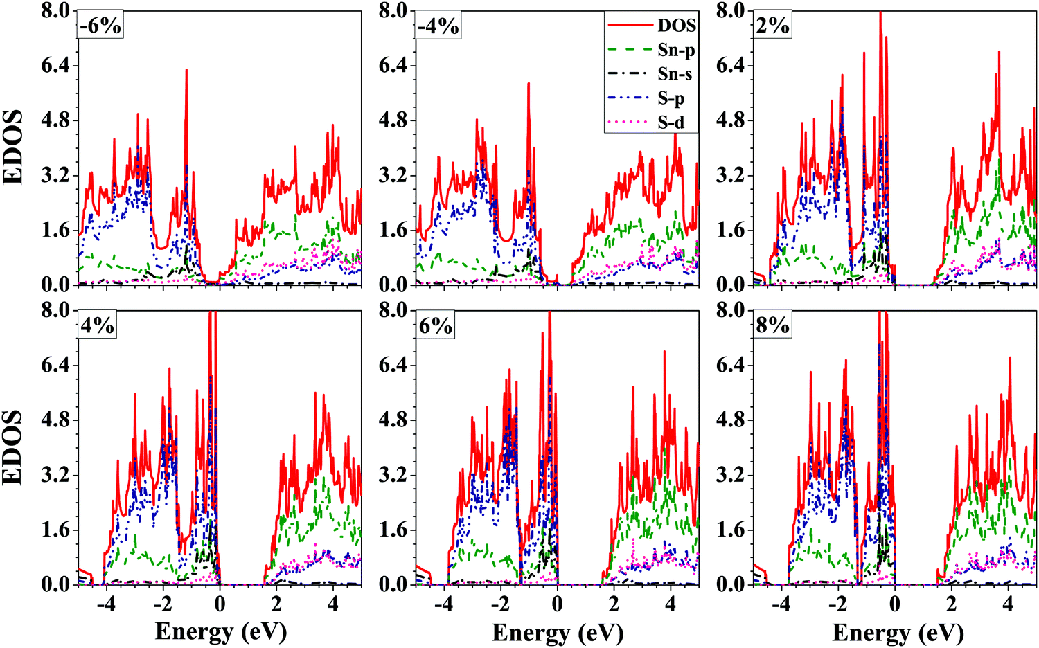 | ||
| Fig. 5 Electronic density of states (EDOS) of the SnS bilayer under different isotropic strains. The VBM has significant contributions due to the p-orbitals of the S-atoms, and the CBM has significant contributions due to the p-orbitals of the Sn-atoms. | ||
From the calculated band structures of the strained bilayer systems, we estimated the effective masses (m*) of the charge carriers, i.e., electrons and holes along the zigzag and armchair directions. The m* values of the electrons (holes) are calculated by fitting the CBM (VBM) to a polynomial function (shown in Fig. S2 of the ESI†). The estimated m* values for the SnS bilayer subjected to different amounts of strain are given in Table 2. Along the zigzag direction, the m* value of the charge carriers decreases with the application of compressive strain whereas it increases with the application of tensile strain to the bilayer. As a result, the mobilities (μ) of charge carriers show higher values for the case of compressive strain compared with the case of tensile strain (Table 2). The deformation potential constant (Eβ) of the charge carriers along the zigzag and armchair directions are calculated for the strained bilayer systems by fitting the change in energy of the CBM (VBM) vs. the uniaxial strain curve (shown in Fig. S3 of ESI†). The results are given in Table 2. Along the zigzag direction, the Eβ value of electrons increases whereas the Eβ of holes decreases with the increase in strain value from −4% to 8%. However, along the armchair direction, the Eβ value of both electrons and holes decreases with the increase in strain value. We further calculated the elastic constants (Cβ) of the strained bilayer systems along the zigzag and armchair directions by fitting the total energy change (E − E0) vs. the uniaxial strain curve to a quadratic polynomial (shown in Fig. S4 of the ESI†). The calculated Cβ values are given in Table 1. The Cβ of the SnS bilayer along the both zigzag and armchair directions decreases with the increase in strain value from −4% to 8% within the error limits.
From the calculated m*, Eβ, and Cβ values, we estimated the relaxation times (τ) of the charge carriers along the zigzag and armchair directions for the SnS bilayer subjected to different amounts of strain using the eqn (2). The calculated values of τ are given in Table 2. The calculated τ values of the charge carriers show anisotropy along the zigzag and armchair directions. Furthermore, from the calculated τ, we estimated the mobilities of the charge carriers using the expression 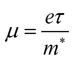 , and the results are given in Table 2. At room temperature, our predicted mobilities of charge carriers along the zigzag directions (154–32
![[thin space (1/6-em)]](https://www.rsc.org/images/entities/char_2009.gif) 381 cm2 V−1 s−1) for the strain range −4% to 2% are quite high compared with other two-dimensional materials like MoS2 (72–73.58 cm2 V−1 s−1)67 and phosphorene (286 cm2 V−1 s−1).68
381 cm2 V−1 s−1) for the strain range −4% to 2% are quite high compared with other two-dimensional materials like MoS2 (72–73.58 cm2 V−1 s−1)67 and phosphorene (286 cm2 V−1 s−1).68
Using the τ values computed above using deformation potential theory, we calculated the electronic transport coefficients (S, σ, and κe) for the strained bilayer systems. Since the SnS bilayer becomes a metal when the compressive strain is 6% or more, and metal is usually not a good thermoelectric material, we have only focussed on the thermoelectric properties of the strained bilayer within the strain range of −4% to 8%. Fig. 6 shows the calculated room-temperature σ values as a function of the carrier concentration (n) along the zigzag and armchair directions for the SnS bilayer subjected to the different amounts of strain. Negative values of n represent an n-type charge-carrier concentration and positive values of n represent a p-type charge-carrier concentration. From Fig. 6, it can be seen that σ is higher for the n-type SnS bilayer compared with the p-type SnS bilayer along the both zigzag and armchair directions. This is due to the higher electron mobilities compared with holes along the zigzag and armchair directions.
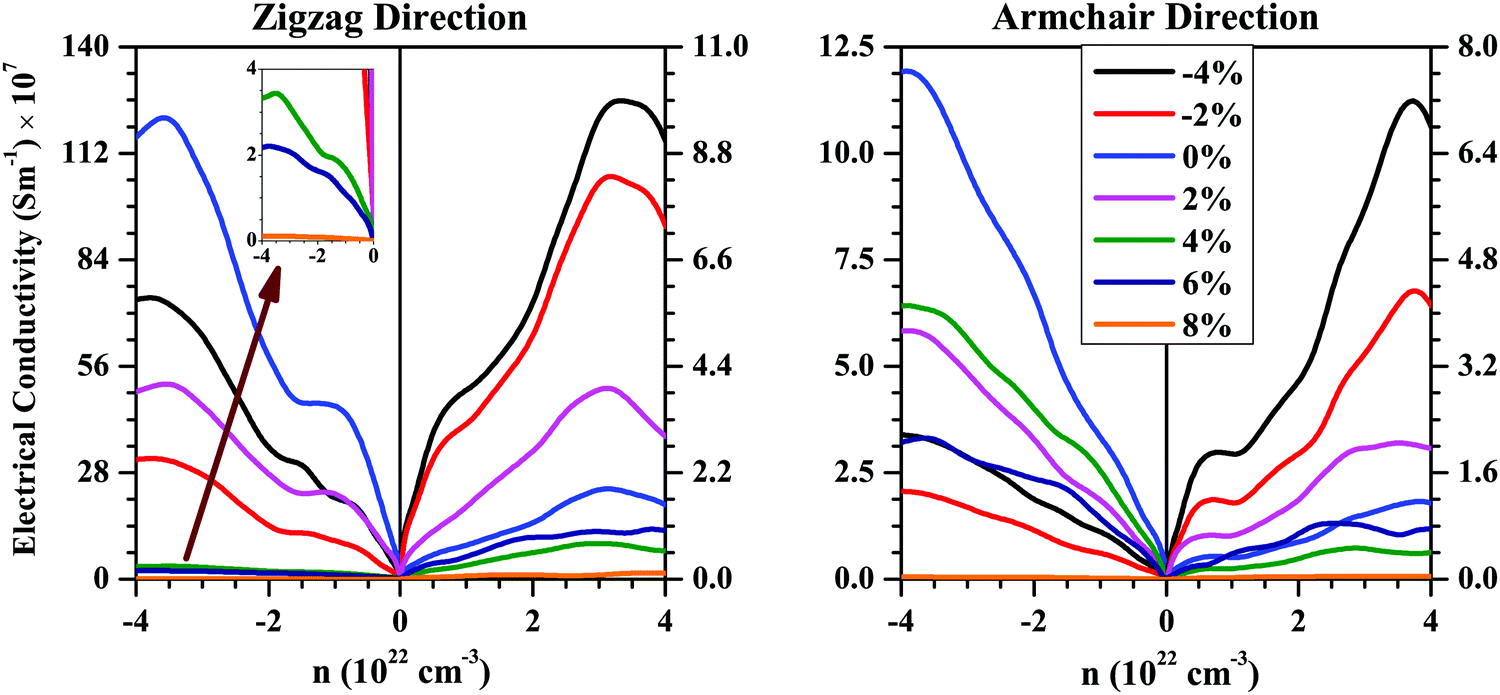 | ||
| Fig. 6 Room-temperature electronic charge conductivity (σ) as a function of the charge-carrier concentration (n) along the zigzag and armchair directions for the SnS bilayer under different isotropic strains. The σ along the zigzag direction is higher compared with σ along the armchair direction due to the higher charge-carrier mobilities along the zigzag direction as compared with the armchair direction. The inset in (a) shows the behaviour of σ for the strain range 6–8%. | ||
The unstrained bilayer has a better σ value compared with the strained bilayer systems for the n-type case along the both zigzag and armchair directions, which is due to the higher electron mobilities for the unstrained bilayer compared with the strained bilayer systems. The compressive strain enhances the holes mobilities (due to the decrease in m* values of the holes) along the both zigzag and armchair directions (Table 2). As a result, the bilayer subjected to compressive strain shows better σ values compared with the unstrained bilayer for the p-type charge-carrier concentration.
Fig. S5 of the ESI† shows the room-temperature κe values as a function of n along the zigzag and armchair directions for the SnS bilayer subjected to different strains. The κe values show a dispersed behaviour along the zigzag and armchair directions for both n-type and p-type charge-carrier concentrations. The κe value is related to σ via the Wiedmann–Franz law (κe = LσT) as discussed in Section 1. Thus, the κevs. n plot follows similar trends as followed by the σ vs. n plot for all the strained bilayer systems.
The calculated peak values of the Seebeck coefficient (S) as a function of temperature (T) for the strained bilayer systems along the zigzag and armchair directions are given in Fig. 7. The S value decreases with the rise in temperature due to the bipolar conduction effect.69 The application of strain tunes the band gap (Eg) of the bilayer (Table 1) and since S ∝ Eg,70 and the plot of S vs. T shows the maximum value for the strained system with the maximum band gap, i.e., for 6% strain. Thus, we can say that the S value is efficiently tuned via band-structure engineering using strain.
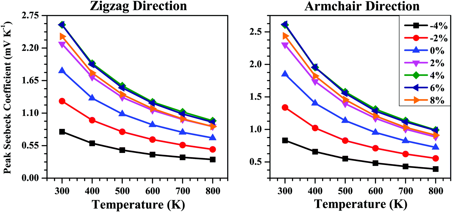 | ||
| Fig. 7 Peak Seebeck coefficient (S) as a function of temperature along the zigzag and armchair directions for the SnS bilayer under different isotropic strains. The S data show higher values for tensile strain compared with compressive strain due to the larger bandgaps for the tensile strain condition (see Table 1) since S ∝ Eg. | ||
The σ value generally decreases with the increase in band gap (Eg), which is in contrast to the tendency of S. Thus, whether the applied strain will benefit the electronic transport properties or not will be determined by the competition between these two factors. The combined effect of S and σ is calculated in terms of the power factor (S2σ). The calculated power factor of the SnS bilayer at different strains as a function of temperature along the zigzag and armchair directions is shown in Fig. 8. With an increase in temperature, the power factor of all the strained bilayer systems decreases and becomes saturated at higher temperatures. The unstrained SnS bilayer has the highest power factor compared with the strained bilayer systems. Among the strained bilayer systems, the maximum power factor along the zigzag direction occurs for the −4% strain case for which the increase in σ has outweighed the negative effect due to the decrease in S. Along the armchair direction, the maximum power factor among the strained bilayer systems occurs for the 4% strain, which indicates that a better tradeoff between the increase in S and the decrease in σ has occurred, maximizing the power factor at 4% strain.
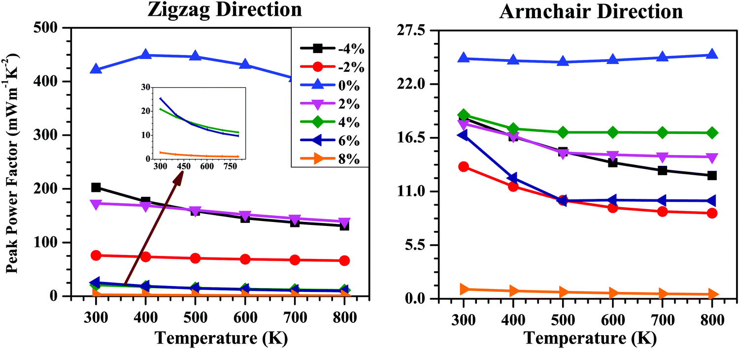 | ||
| Fig. 8 Peak power factor (S2σ) as a function of temperature along the zigzag and armchair directions for the SnS bilayer under different isotropic strains. With the rise in temperature, the power factor of the bilayer at different strains decreases and gets saturated at higher temperatures. The inset in figure shows the behaviour of power factor for the strain range 4–8% along the zigzag direction. | ||
Next, we studied the strain effect on the thermal transport properties of the SnS bilayer. The lattice thermal conductivities (κl) of the unstrained and strained bilayer systems along the armchair and zigzag directions are shown in Fig. 9. For all the cases, the κl value decreases with an increase in temperature, following a T−1 dependence, as indicated by the fitting lines in Fig. 9. Thus, the dominant scattering mechanism is the Umklapp process.32 Usually, the main contribution to κl is from the acoustic phonon modes. The lower the phonon frequencies of the acoustic modes, the lower will be the phonon group velocities, which in turn will lead to smaller κl values. So, we noted the maximum phonon frequencies of the acoustic phonon modes (νmax) for the strained bilayer systems and tried to relate them to their corresponding κl values.
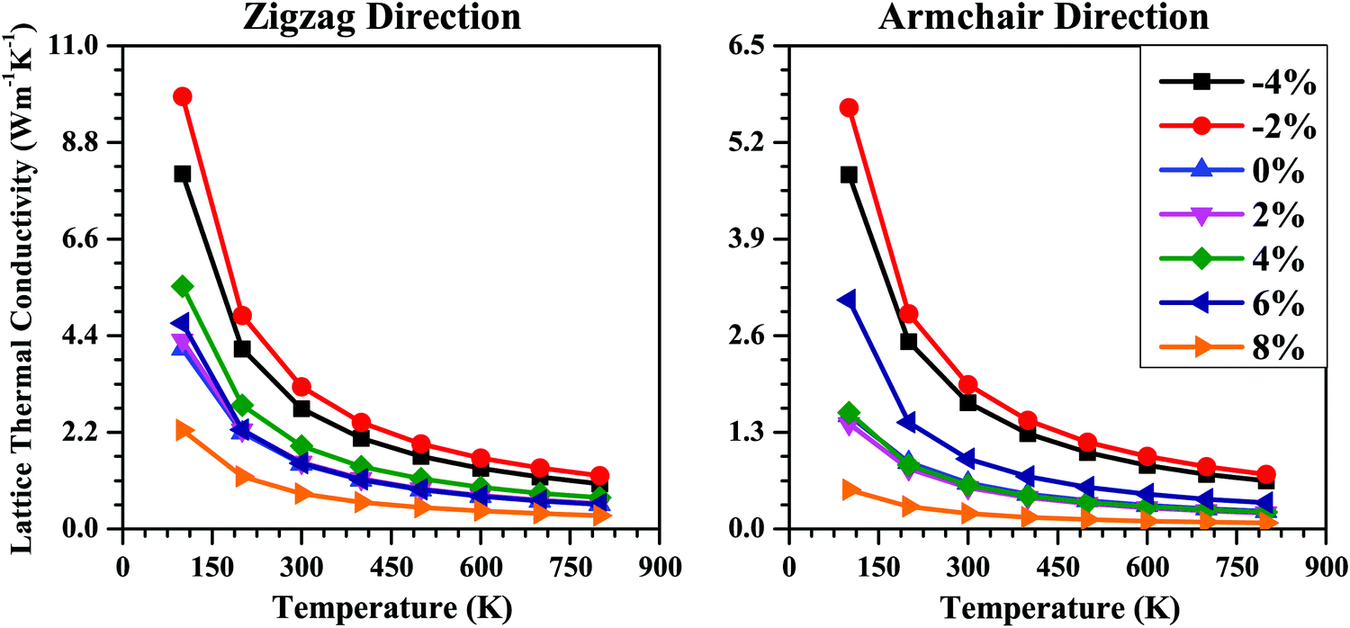 | ||
| Fig. 9 Lattice thermal conductivity (κl) as a function of temperature in the range 100 to 800 K along the zigzag and armchair directions for the SnS bilayer under different isotropic strains. With the increase in strain from −4% to 8%, the κl of the bilayer decreases. | ||
The νmax value for the unstrained bilayer is 0.24 THz; the νmax values for compressive strains of −4% and −2% are 0.28 THz and 0.26 THz, respectively; whereas for tensile strains of 2%, 4%, 6% and 8%, the νmax values are 0.24 THz, 0.24 THz, 0.24 THz, and 0.23 THz, respectively. Due to the higher νmax values for compressive strain compared with tensile strain, the calculated κl values for compressive strain are higher than the κl values for tensile strain (Fig. 9). Due to the similar νmax values for the 0–6% strain range, the calculated κl values for this range are nearly equal (Fig. 9). Furthermore, due to the lowest νmax values being for the 8% strain among all the strain values, the κl value for the 8% strain case is the minimum among all the cases. Furthermore, the calculated νmax values for the strained SnS bilayer systems (0.23–0.28 THz) are much smaller than other 2D materials such as MoS2 (7.5 THz)71 and MoSe2 (4.8 THz).72 As a result, the room-temperature κl values for the strained SnS bilayers (0.21–3.23 W m−1 K−1) are much smaller than these 2D materials, i.e., MoS2 (100 W m−1 K−1) and MoSe2 (40 W m−1 K−1).71,72
Combining the electronic and thermal transport properties, we finally evaluated the thermoelectric performance of the SnS bilayer at different strains in terms of their figure of merit (ZT) data. The calculated peak values of ZT as a function of temperature for the SnS bilayer at different strains are shown in Fig. 10. For the unstrained bilayer, the peak values of ZT at room temperature are 0.93 and 1.18 along the zigzag and armchair directions, respectively. The application of isotropic strain improves the thermoelectric performance of the bilayer. Along the zigzag direction, the highest ZT value occurred at 2% strain, with a peak value of 4.96 at room temperature, which is 5.3 times higher than the peak ZT of the unstrained bilayer along the zigzag direction. Along the armchair direction, the highest ZT value occurred for the 4% strain, with a peak value of 2.40 at room temperature, which is 2.03 times higher than the peak ZT of the unstrained bilayer along the armchair direction. These high ZT values obtained at the 2% and 4% strains are the result of the combined effect of a high Seebeck coefficient and a low κl value at these strains. Such high ZT values are highly desirable for the fabrication of thermoelectric modules for practical applications.
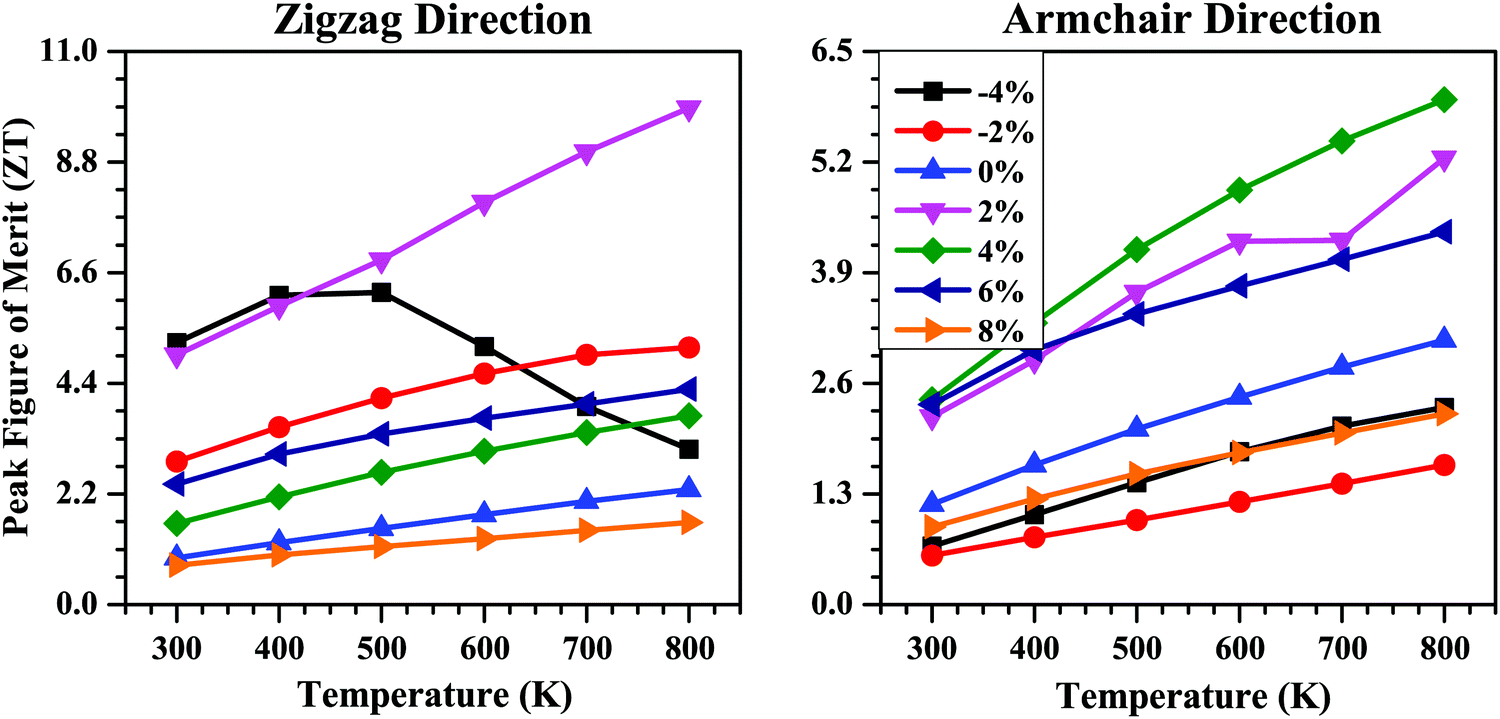 | ||
| Fig. 10 Peak figure of merit (ZT) as a function of temperature along the zigzag and armchair directions for the SnS bilayer under different isotropic strains. The peak ZT of the bilayer shows higher values for the strained bilayer cases compared with the pristine SnS bilayer. | ||
4 Conclusion
Using first-principles calculations and Boltzmann transport theory, we have explored the isotropic strain effect on the electronic and thermoelectric properties of the SnS bilayer. Our results indicate that the bilayer has a “pudding-mould-type” band structure with the band gap of 1.12 eV. At a compressive isotropic strain, the band gap is decreased, and metallicity emerges when the compressive strain reaches 6% or larger. By contrast, the band gap first increases and then decreases for increasing tensile strain, reaching a maximum at a strain of 6%. The Seebeck coefficient along the zigzag and armchair directions shows improved values for tensile strain. The low frequency of the acoustic phonon modes and the coupling between the acoustic and optical phonon modes makes the lattice thermal conductivity of the bilayer low. With tensile strain, the maximum phonon frequency of the acoustic phonon modes is decreased compared with compressive strain, leading to lower lattice thermal conductivities for tensile strain compared with compressive strain. Due to the combined effect of the increased Seebeck coefficients and low lattice thermal conductivities for tensile strain, the calculated ZT values for tensile strain show higher values compared with compressive strain. At room temperature, the maximum ZT value along the zigzag direction occurred for the 2% strain with a value of 4.96, and along the armchair direction the maximum ZT at room temperature occurred for the 4% strain with a value of 2.40. These ZT values are much higher than the room-temperature ZT values of the unstrained bilayer, which are 0.93 and 1.18 along the zigzag and armchair directions, respectively. Our results show that applied strain is an efficient method for improving the thermoelectric performance of the SnS bilayer.In experiments, strain can be applied to 2D materials in different ways. For example, strain can be induced by a lattice mismatch between the epitaxial thin film and substrate.73 Moreover, one can transfer a 2D material to a soft supporting substrate and apply strain to the 2D material by bending74 or stretching75 the substrate. Hui et al. have reported an electromechanical device that can apply biaxial compressive strain to atomically thin MoS2 supported on a piezoelectric substrate.76 Since the SnS system studied in our work is a very promising candidate for thermoelectric applications, we expect experimentalists to develop techniques for studying these systems via experiment.
Conflicts of interest
There are no conflicts to declare.Acknowledgements
This project was funded by the Deanship of Scientific Research (DSR) King Abdulaziz University, Jeddah, Saudi Arabia under Grant No. (KEP-50-130-42). The authors therefore acknowledge with thanks DSR for technical and financial support. Also, the authors are thankful to the National PARAM-Yuva-II supercomputing facility at the Center for Development of Advanced Computing, Pune, India and King Abdulaziz University's High-Performance Computing Center (Aziz Supercomputer) (http://hpc.kau.edu.sa) for providing the computational resources. Shagun Nag thanks the Department of Science and Technology, India for financial support under DST/INSPIRE Fellowship [IF170923].References
- S. Chu and A. Majumdar, Nature, 2012, 488, 294–303 CrossRef CAS PubMed.
- K. Uchida, S. Takahashi, K. Harii, J. Ieda, W. Koshibae, K. Ando, S. Maekawa and E. Saitoh, Nature, 2008, 455, 778–781 CrossRef CAS PubMed.
- B. C. Sales, Curr. Opin. Solid State Mater. Sci., 1997, 2, 284–289 CrossRef CAS.
- L. E. Bell, Science, 2008, 321, 1457–1461 CrossRef CAS PubMed.
- G. J. Snyder and E. S. Toberer, Mater. Renew. Sustain. Energy, 2011, 101–110 Search PubMed.
- L. D. Hicks and M. S. Dresselhaus, Phys. Rev. B: Condens. Matter Mater. Phys., 1993, 47, 16631 CrossRef CAS PubMed.
- N. Stojanovic, D. Maithripala, J. Berg and M. Holtz, Phys. Rev. B: Condens. Matter Mater. Phys., 2010, 82, 075418 CrossRef.
- L. D. Zhao, V. P. Dravid and M. G. Kanatzidis, Energy Environ. Sci., 2014, 7, 251–268 RSC.
- J. He and T. M. Tritt, Science, 2017, 357, 6358 Search PubMed.
- T. G. Novak, K. Kim and S. Jeon, Nanoscale, 2019, 11, 19684–19699 RSC.
- F. Xiong, H. B. Tan, C. Xia and Y. Chen, ACS Appl. Nano Mater., 2019, 3, 114–119 CrossRef.
- R. Moshwan, W. D. Liu, X. L. Shi, Y. P. Wang, J. Zou and Z. G. Chen, Nano Energy, 2019, 65, 104056 CrossRef CAS.
- Q. Zhang, Q. Song, X. Wang, J. Sun, Q. Zhu, K. Dahal, X. Lin, F. Cao, J. Zhou and S. Chen, et al. , Energy Environ. Sci., 2018, 11, 933–940 RSC.
- C. Wan, R. Tian, M. Kondou, R. Yang, P. Zong and K. Koumoto, Nat. Commun., 2017, 8, 1–9 CrossRef CAS.
- M. S. Dresselhaus, G. Chen, M. Y. Tang, R. Yang, H. Lee, D. Wang, Z. Ren, J. P. Fleurial and P. Gogna, Adv. Mater., 2007, 19, 1043–1053 CrossRef CAS.
- C. Xin, J. Zheng, Y. Su, S. Li, B. Zhang, Y. Feng and F. Pan, J. Phys. Chem. C, 2016, 120, 22663–22669 CrossRef CAS.
- M. Sun, J. P. Chou, L. Shi, J. Gao, A. Hu, W. Tang and G. Zhang, ACS Omega, 2018, 3, 5971–5979 CrossRef CAS PubMed.
- F. Q. Wang, S. Zhang, J. Yu and Q. Wang, Nanoscale, 2015, 7, 15962–15970 RSC.
- R. Gupta, B. Dongre, J. Carrete and C. Bera, J. Appl. Phys., 2021, 130, 054301 CrossRef CAS.
- Y. Li, K. Ma, X. Fan, F. Liu, J. Li and H. Xie, Appl. Surf. Sci., 2020, 521, 146256 CrossRef CAS.
- B. Ul Haq, S. AlFaify and A. Laref, J. Phys. Chem. C, 2019, 123, 18124–18131 CrossRef CAS.
- L. D. Zhao, S. H. Lo, Y. Zhang, H. Sun, G. Tan, C. Uher, C. Wolverton, V. P. Dravid and M. G. Kanatzidis, Nature, 2014, 508, 373–377 CrossRef CAS PubMed.
- Z. G. Chen, X. Shi, L. D. Zhao and J. Zou, Prog. Mater. Sci., 2018, 97, 283–346 CrossRef CAS.
- A. Banik, S. Roychowdhury and K. Biswas, Chem. Commun., 2018, 54, 6573–6590 RSC.
- J. P. Heremans, V. Jovovic, E. S. Toberer, A. Saramat, K. Kurosaki, A. Charoenphakdee, S. Yamanaka and G. J. Snyder, Science, 2008, 321, 554–557 CrossRef CAS.
- M. J. Lee, J. H. Ahn, J. H. Sung, H. Heo, S. G. Jeon, W. Lee, J. Y. Song, K. H. Hong, B. Choi and S. H. Lee, et al. , Nat. Commun., 2016, 7, 1–7 CAS.
- A. Shafique and Y. H. Shin, Sci. Rep., 2017, 7, 1–10 CrossRef CAS.
- D. Wickramaratne, F. Zahid and R. K. Lake, J. Appl. Phys., 2015, 118, 075101 CrossRef.
- D. Wickramaratne, F. Zahid and R. K. Lake, J. Chem. Phys., 2014, 140, 124710 CrossRef PubMed.
- G. Mahan and L. Woods, Phys. Rev. Lett., 1998, 80, 4016 CrossRef CAS.
- S. D. Guo, J. Mater. Chem. C, 2016, 4, 9366–9374 RSC.
- H. Lv, W. Lu, D. Shao, H. Lu and Y. Sun, J. Mater. Chem. C, 2016, 4, 4538–4545 RSC.
- G. Li, K. Yao and G. Gao, Nanotechnology, 2017, 29, 015204 CrossRef PubMed.
- E. Witkoske, D. Guzman, Y. Feng, A. Strachan, M. Lundstrom and N. Lu, J. Appl. Phys., 2019, 125, 082531 CrossRef.
- R. Roldán, A. Castellanos Gomez, E. Cappelluti and F. Guinea, J. Phys.: Condens. Matter, 2015, 27, 313201 CrossRef PubMed.
- D. Qin, X. J. Ge, G. Q. Ding, G. Y. Gao and J. T. Lü, RSC Adv., 2017, 7, 47243–47250 RSC.
- Y. Y. Zhang, Q. X. Pei, J. W. Jiang, N. Wei and Y. W. Zhang, Nanoscale, 2016, 8, 483–491 RSC.
- A. X. Zhang, J. T. Liu, S. D. Guo and H. C. Li, Phys. Chem. Chem. Phys., 2017, 19, 14520–14526 RSC.
- T. V. Vu, V. T. Vi, H. V. Phuc, C. V. Nguyen, N. Poklonski, C. Duque, D. Rai, B. D. Hoi and N. N. Hieu, J. Phys.: Condens. Matter, 2021, 33, 225503 CrossRef CAS.
- Y. Cai, G. Zhang and Y. W. Zhang, Sci. Rep., 2014, 4, 1–6 Search PubMed.
- A. Manjanath, A. Samanta, T. Pandey and A. K. Singh, Nanotechnology, 2015, 26, 075701 CrossRef CAS.
- G. Kresse and J. Furthmüller, Comput. Mater. Sci., 1996, 6, 15–50 CrossRef CAS.
- G. Kresse and J. Hafner, Phys. Rev. B: Condens. Matter Mater. Phys., 1994, 49, 14251–14269 CrossRef CAS PubMed.
- P. Giannozzi, S. Baroni, N. Bonini, M. Calandra, R. Car, C. Cavazzoni, D. Ceresoli, G. L. Chiarotti, M. Cococcioni and I. Dabo, et al. , J. Phys.: Condens. Matter, 2009, 21, 395502 CrossRef.
- J. P. Perdew, K. Burke and M. Ernzerhof, Phys. Rev. Lett., 1996, 77, 3865 CrossRef CAS PubMed.
- J. Heyd, G. E. Scuseria and M. Ernzerhof, J. Chem. Phys., 2003, 118, 8207–8215 CrossRef CAS.
- H. J. Monkhorst and J. D. Pack, Phys. Rev. B: Solid State, 1976, 13, 5188 CrossRef.
- S. Grimme, J. Comput. Chem., 2006, 27, 1787–1799 CrossRef CAS PubMed.
- K. Kaur, D. Murali and B. Nanda, J. Mater. Chem. A, 2019, 7, 12604–12615 RSC.
- G. K. Madsen and D. J. Singh, Comput. Phys. Commun., 2006, 175, 67–71 CrossRef CAS.
- J. Bardeen and W. Shockley, Phys. Rev., 1950, 80, 72–80 CrossRef CAS.
- S. Nag, R. Singh and R. Kumar, J. Phys.: Condens. Matter, 2021, 33, 315705 CrossRef CAS PubMed.
- L. C. Zhang, G. Qin, W. Z. Fang, H. J. Cui, Q. R. Zheng, Q. B. Yan and G. Su, Sci. Rep., 2016, 6, 19830 CrossRef CAS PubMed.
- S. Nag, A. Saini, R. Singh and R. Kumar, Appl. Surf. Sci., 2020, 512, 145640 CrossRef CAS.
- A. Togo, F. Oba and I. Tanaka, Phys. Rev. B: Condens. Matter Mater. Phys., 2008, 78, 134106 CrossRef.
- A. Togo, L. Chaput and I. Tanaka, Phys. Rev. B: Condens. Matter Mater. Phys., 2015, 91, 094306 CrossRef.
- R. J. Hardy, Phys. Rev., 1963, 132, 168 CrossRef.
- J. Carrete, B. Vermeersch, A. Katre, A. van Roekeghem, T. Wang, G. K. Madsen and N. Mingo, Comput. Phys. Commun., 2017, 220, 351–362 CrossRef CAS.
- L. Chaput, Phys. Rev. Lett., 2013, 110, 265506 CrossRef PubMed.
- M. Simoncelli, N. Marzari and F. Mauri, Nat. Phys., 2019, 15, 809–813 Search PubMed.
- Q. Zhang, X. Chen, W. C. Liu and Y. Wang, Comput. Mater. Sci., 2019, 158, 272–281 CrossRef CAS.
- H. Usui and K. Kuroki, J. Appl. Phys., 2017, 121, 165101 CrossRef.
- H. Usui, K. Suzuki, K. Kuroki, S. Nakano, K. Kudo and M. Nohara, Phys. Rev. B: Condens. Matter Mater. Phys., 2013, 88, 075140 CrossRef.
- S. Wei, C. Wang, S. Fan and G. Gao, J. Appl. Phys., 2020, 127, 155103 CrossRef CAS.
- H. Lv, W. Lu, D. Shao and Y. Sun, Phys. Rev. B: Condens. Matter Mater. Phys., 2014, 90, 085433 CrossRef CAS.
- Y. Pei, X. Shi, A. LaLonde, H. Wang, L. Chen and G. J. Snyder, Nature, 2011, 473, 66–69 CrossRef CAS PubMed.
- A. Rawat, N. Jena and A. De Sarkar, et al. , J. Mater. Chem. A, 2018, 6, 8693–8704 RSC.
- H. Liu, A. T. Neal, Z. Zhu, Z. Luo, X. Xu, D. Tománek and P. D. Ye, ACS Nano, 2014, 8, 4033–4041 CrossRef CAS PubMed.
- H. Shi, D. Parker, M. H. Du and D. J. Singh, Phys. Rev. Appl., 2015, 3, 014004 CrossRef CAS.
- V. Johnson and K. Lark Horovitz, Phys. Rev., 1953, 92, 226 CrossRef CAS.
- Z. Jin, Q. Liao, H. Fang, Z. Liu, W. Liu, Z. Ding, T. Luo and N. Yang, Sci. Rep., 2015, 5, 1–7 Search PubMed.
- S. Kumar and U. Schwingenschlogl, Chem. Mater., 2015, 27, 1278–1284 CrossRef CAS.
- G. Gao, S. Jin and W. Wu, Appl. Phys. Lett., 2007, 90, 012509 CrossRef.
- S. I. Park, J. H. Ahn, X. Feng, S. Wang, Y. Huang and J. A. Rogers, Adv. Funct. Mater., 2008, 18, 2673–2684 CrossRef CAS.
- K. S. Kim, Y. Zhao, H. Jang, S. Y. Lee, J. M. Kim, K. S. Kim, J. H. Ahn, P. Kim, J. Y. Choi and B. H. Hong, Nature, 2009, 457, 706–710 CrossRef CAS PubMed.
- Y. Y. Hui, X. Liu, W. Jie, N. Y. Chan, J. Hao, Y. T. Hsu, L. J. Li, W. Guo and S. P. Lau, ACS Nano, 2013, 7, 7126–7131 CrossRef CAS PubMed.
Footnote |
| † Electronic supplementary information (ESI) available. See DOI: 10.1039/d1cp03988a |
| This journal is © the Owner Societies 2022 |